 | –≠–ª–µ–∫—Ç—Ä–æ–Ω–Ω—ã–π –∫–æ–º–ø–æ–Ω–µ–Ω—Ç: RF2619 | –°–∫–∞—á–∞—Ç—å:  PDF PDF  ZIP ZIP |
¸
10-25
10
IF
AMP
L
IE
R
S
Product Description
Ordering Information
Typical Applications
Features
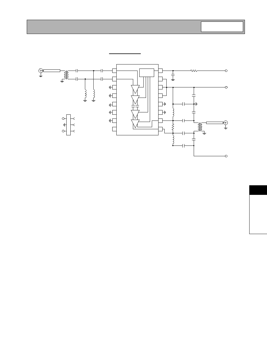
Functional Block Diagram
RF Micro Devices, Inc.
7628 Thorndike Road
Greensboro, NC 27409, USA
Tel (336) 664 1233
Fax (336) 664 0454
http://www.rfmd.com
Optimum Technology MatchingÆ Applied
Si BJT
GaAs MESFET
GaAs HBT
Si Bi-CMOS
SiGe HBT
Si CMOS
1
2
3
4
5
6
7
8
16
15
14
13
12
11
10
9
CDMA+
CDMA-
GND
GND
GND
GND
GND
NC
GC
VCC
VCC
VCC
GND
GND
OUT+
OUT-
GAIN
CONTROL
0.157
0.150
0.025
0.012
0.008
0.196
0.189
0.2440
0.2284
0.0688
0.0532
0.050
0.016
0.0098
0.0075
8∞ MAX
0∞MIN
NOTES:
1. Shaded lead is Pin 1.
2. All dimensions are excluding mold flash.
3. Lead coplanarity - 0.005 with respect to datum "A".
-A-
0.0098
0.0040
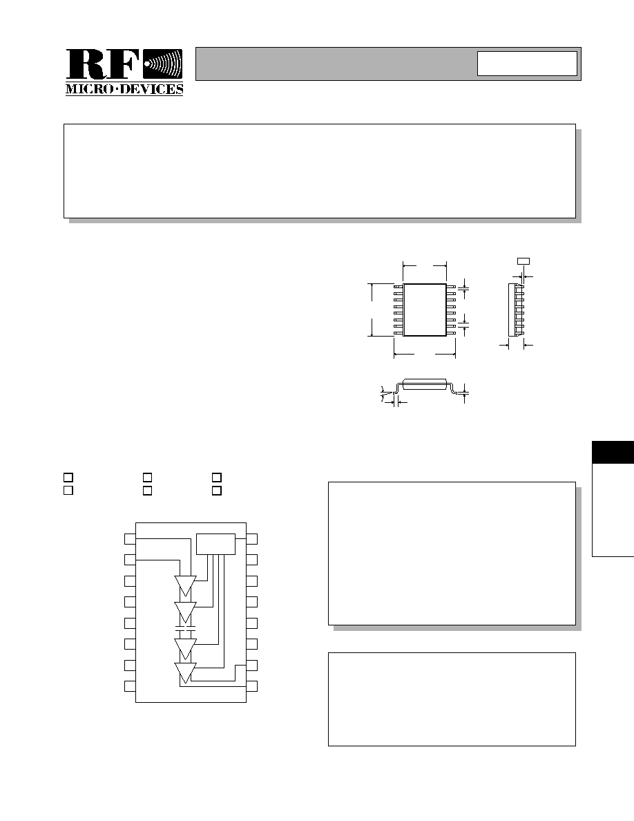
RF2619
3V CDMA/FM TRANSMIT AGC AMPLIFIER
∑ 3V CDMA/FM Cellular Systems
∑ Supports Dual-Mode AMPS/CDMA
∑ Supports Dual-Mode TACS/CDMA
∑ General Purpose Linear IF Amplifier
∑ Portable Battery-Powered Equipment
∑ Commercial and Consumer Systems
The RF2619 is a complete AGC amplifier designed for
the transmit section of 3V dual-mode CDMA/FM cellular
applications. It is designed to amplify IF signals while pro-
viding more than 84dB of gain control range. Noise Fig-
ure, IP3, and other specifications are designed to be
compatible with the IS-95 Interim Standard for CDMA cel-
lular communications. This circuit is designed as part of
the RFMD CDMA Chip Set, consisting of this Transmit IF
AGC Amp, a Transmit Upconverter, a Receive LNA/Mixer,
and a Receive IF AGC Amp. The IC is manufactured on
an advanced high frequency Silicon Bipolar process and
is packaged in a standard miniature 16-lead plastic SSOP
package.
∑ Supports Dual Mode Operation
∑ -48dB to +42dB Gain Control Range
∑ Single 3V Power Supply
∑ Monolithic Construction
∑ 12MHz to 175MHz Operation
∑ Miniature Surface Mount Package
RF2619
3V CDMA/FM Transmit AGC Amplifier
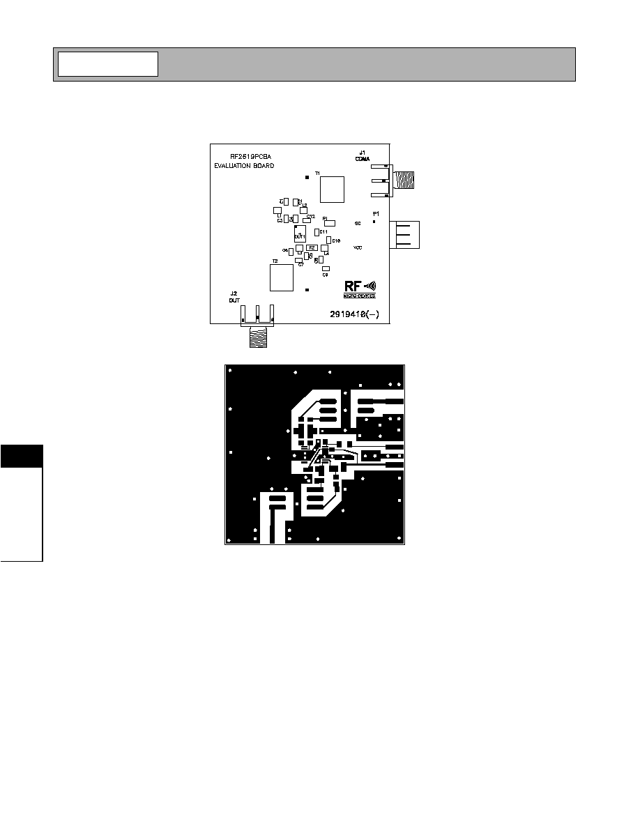
RF2619 PCBA
Fully Assembled Evaluation Board
10
Rev B5 010720
Package Style: SSOP-16
10-26
RF2619
Rev B5 010720
10
IF
AMP
L
IE
R
S
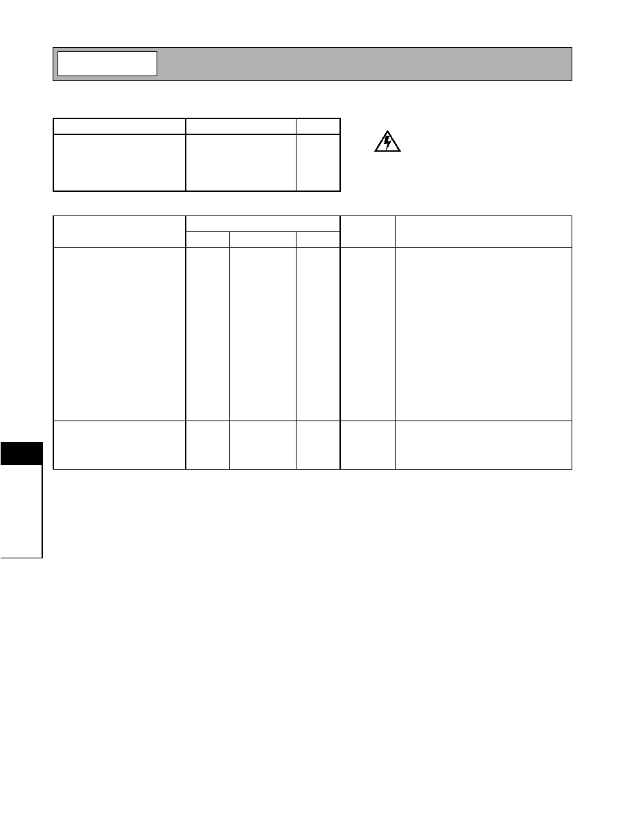
Absolute Maximum Ratings
Parameter
Rating
Unit
Supply Voltage
-0.5 to +7.0
V
DC
Control Voltage
-0.5 to +5.0
V
Input Power Levels
+10
dBm
Operating Ambient Temperature
-40 to +85
∞C
Storage Temperature
-40 to +150
∞C
Parameter
Specification
Unit
Condition
Min.
Typ.
Max.
Overall
T = 25∞C, 130MHz, V
CC
=3.0V, Pin=-
40dBm, Z
S
=1k
, Z
L
=1k
, 1k
External
Output Terminating Resistor (Effective
Z
L
= 500
) (See Application Example)
Frequency Range
12 to 175
MHz
Maximum Gain
+39
+42
dB
V
GC
=2.4V
Minimum Gain
-48
-45
dB
V
GC
= 0.3V
Gain Slope
57
dB/V
Measured in 0.5V increments
Gain Control Voltage Range
0 to 3
V
DC
Gain Control Input Impedance
30
k
Noise Figure
10.5
13
dB
At maximum gain and 130MHz
Input IP3
-26
-25
dBm
At +10 gain and referenced to 1k
,
Pin=-45dBm per tone
Input Impedance
1
k
Differential
Stability (Max VSWR)
10:1
Spurious< -70dBm
Power Supply
Voltage
2.7 to 3.3
V
Current Consumption
23
25
mA
Maximum gain, V
CC
= 3.0V
Current Consumption
22
24
mA
Minimum gain, V
CC
= 3.0V
Caution! ESD sensitive device.
RF Micro Devices believes the furnished information is correct and accurate
at the time of this printing. However, RF Micro Devices reserves the right to
make changes to its products without notice. RF Micro Devices does not
assume responsibility for the use of the described product(s).
10-27
RF2619
Rev B5 010720
10
IF
AMP
L
IE
R
S
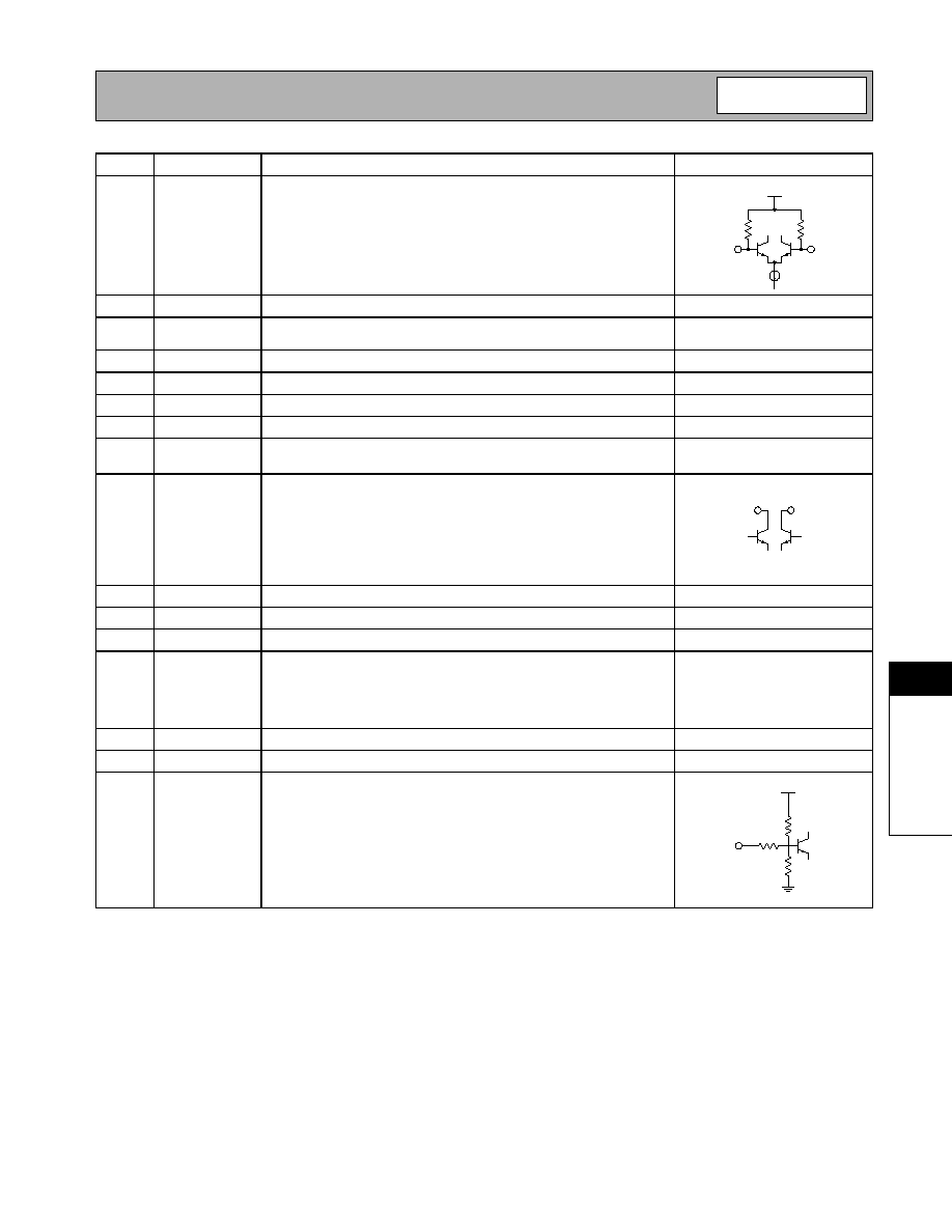
Pin
Function
Description
Interface Schematic
1
CDMA+
CDMA balanced input pin. This pin is internally DC-biased and should
be DC-blocked if connected to a device with a DC level, other than V
CC
,
present. A DC to connection to V
CC
is acceptable. For single-ended
input operation, one pin is used as an input and the other CDMA input
is AC-coupled to ground. The balanced input impedance is 1k
, while
the single-ended input impedance is 500
.
2
CDMA-
Same as pin 2, except complementary input.
See pin 1 schematic.
3
GND
Ground connection. For best performance, keep traces physically short
and connect immediately to ground plane.
4
GND
Same as pin 3.
5
GND
Same as pin 3.
6
GND
Same as pin 3.
7
GND
Same as pin 3.
8
NC
No Connection pin. This pin is internally biased and should not be con-
nected to any external circuitry, including ground or V
CC
.
9
OUT-
Balanced output pin. This is an open-collector output, designed to
operate into a 500
balanced load. The load sets the operating imped-
ance, but an external choke or matching inductor to V
CC
must also be
supplied in order to correctly bias this output. This bias inductor is typi-
cally incorporated in the matching network between the output and next
stage. Because this pin is biased to V
CC
, a DC-blocking capacitor must
be used if the next stage's input has a DC path to ground.
10
OUT+
Same as pin 9, except complementary output.
See pin 9 schematic.
11
GND
Same as pin 3.
12
GND
Same as pin 3.
13
VCC
Supply Voltage pin. External bypassing is required. The trace length
between the pin and the bypass capacitors should be minimized. The
ground side of the bypass capacitors should connect immediately to
ground plane. Pins 13, 14, and 15 may share one bypass capacitor if
trace lengths are kept minimal.
14
VCC
Same as pin 13.
15
VCC
Same as pin 13.
16
GC
Analog gain adjustment for all amplifiers. Valid control ranges are from
0V to 3.0V. Maximum gain is selected with 3.0V. Minimum gain is
selected with 0V. These voltages are valid only for a 3.3k
DC source
impedance.
580
V
CC
580
CDMA-
CDMA+
OUT-
OUT+
23.5 k
15 k
12.7 k
V
CC
10-28
RF2619
Rev B5 010720
10
IF
AMP
L
IE
R
S
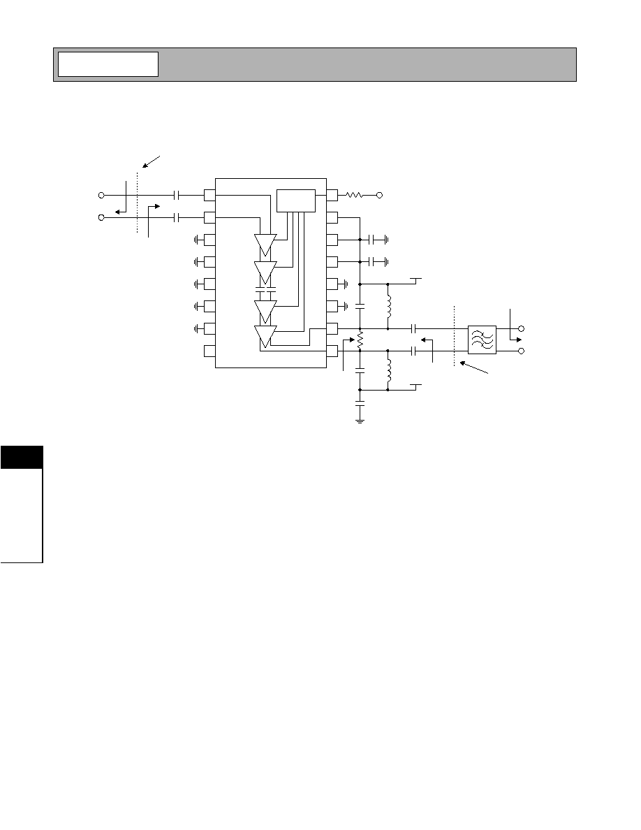
Application Schematic
1
2
3
4
5
6
7
8
16
15
14
13
12
11
10
9
10 nF
10 nF
R2:
1 k
C2
C2
L1
C1
L1
C1
V
CC
10 nF
V
CC
CDMA Filter
OUT+
OUT-
IN+
IN-
Measurement
Reference Plane
Z
IN
=1 k
Z
S
=1 k
Z
OUT
=1 k
Z
LOAD
=1 k
R2 sets the balanced output impedance to 1 k
. L1 and C2
serve dual purposes. L1 serves as an output bias choke,
and C2 serves as a series DC block. In addition, the values
of L1 and C2 may be chosen to form an impedance
matching network if the load impedance is not 1k
.
Otherwise, the values of L1 and C1 are chosen to form a
parallel-resonant tank circuit at the IF when the IF filter's
input impedance is 1 k
.
Z
LOAD,EFF
=500
Measurement
Reference Plane
10 nF
10 nF
3.3 k
GAIN
GAIN
CONTROL
10-29
RF2619
Rev B5 010720
10
IF
AMP
L
IE
R
S
Evaluation Board Schematic
(Download Bill of Materials from www.rfmd.com.)
1
2
3
4
5
6
7
8
16
15
14
13
12
11
10
9
GAIN
CONTROL
T1
C1
5.1 pF
C3
0.01
µ
F
C2
5.1 pF
C4
0.01
µ
F
50
µ
strip
J1
SMA
L2
270 nH
L1
270 nH
R1
3.3 k
C12
0.01
µ
F
P1-3
P1-1
C10
0.01
µ
F
C11
0.01
µ
F
L4
100 nH
C9
20 pF
C8
36 pF
T2
WB3040
R2
1k
C5
36 pF
L3
100 nH
C6
0.01
µ
F
P1-1
C7
20 pF
50
µ
strip
J2
SMA
2619400A
CDMA
OUT
GND
P1-1
VCC
P1-3
GC
1
2
3
P1
10-30
RF2619
Rev B5 010720
10
IF
AMP
L
IE
R
S
Evaluation Board Layout
10-31
RF2619
Rev B5 010720
10
IF
AMP
L
IE
R
S
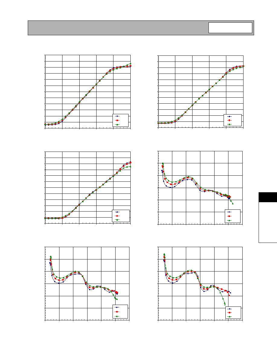
Gain versus Gain Control Voltage
(V
CC
=2.7V, 130MHz)
-60.0
-50.0
-40.0
-30.0
-20.0
-10.0
0.0
10.0
20.0
30.0
40.0
50.0
60.0
0.0
0.5
1.0
1.5
2.0
2.5
GC (V)
Gain
(dB)
-30 C
+25 C
+80 C
RF2619 Gain versus Gain Control Voltage
(V
CC
=3.0 V, 130 MHz)
-60.0
-50.0
-40.0
-30.0
-20.0
-10.0
0.0
10.0
20.0
30.0
40.0
50.0
60.0
0.0
0.5
1.0
1.5
2.0
2.5
GC (volts)
Ga
i
n
(
d
B
)
-30 C
+25 C
+80 C
Gain versus Gain Control Voltage
(V
CC
=3.3 V, 130 MHz)
-60.0
-50.0
-40.0
-30.0
-20.0
-10.0
0.0
10.0
20.0
30.0
40.0
50.0
60.0
0.0
0.5
1.0
1.5
2.0
2.5
GC (V)
Ga
i
n
(
d
B
)
-30 C
+25 C
+ 80 C
IIP3 versus Gain
(V
CC
=2.7 V, 130 MHz)
-50.0
-40.0
-30.0
-20.0
-10.0
0.0
10.0
-60.0
-40.0
-20.0
0.0
20.0
40.0
60.0
Gain (dB)
IIP3
(dB)
-30 C
+25 C
+80 C
IIP3 versus Gain
(V
CC
=3.0 V, 130 MHz)
-50.0
-40.0
-30.0
-20.0
-10.0
0.0
10.0
-60.0
-40.0
-20.0
0.0
20.0
40.0
60.0
Gain (dB)
IIP3
(dB)
-30 C
+25 C
+80 C
IIP3 versus Gain
(V
CC
=3.3 V, 130 MHz)
-50.0
-40.0
-30.0
-20.0
-10.0
0.0
10.0
-60.0
-40.0
-20.0
0.0
20.0
40.0
60.0
Gain (dB)
IIP3
(dB)
-30 C
+25 C
+ 80 C
10-32
RF2619
Rev B5 010720
10
IF
AMP
L
IE
R
S
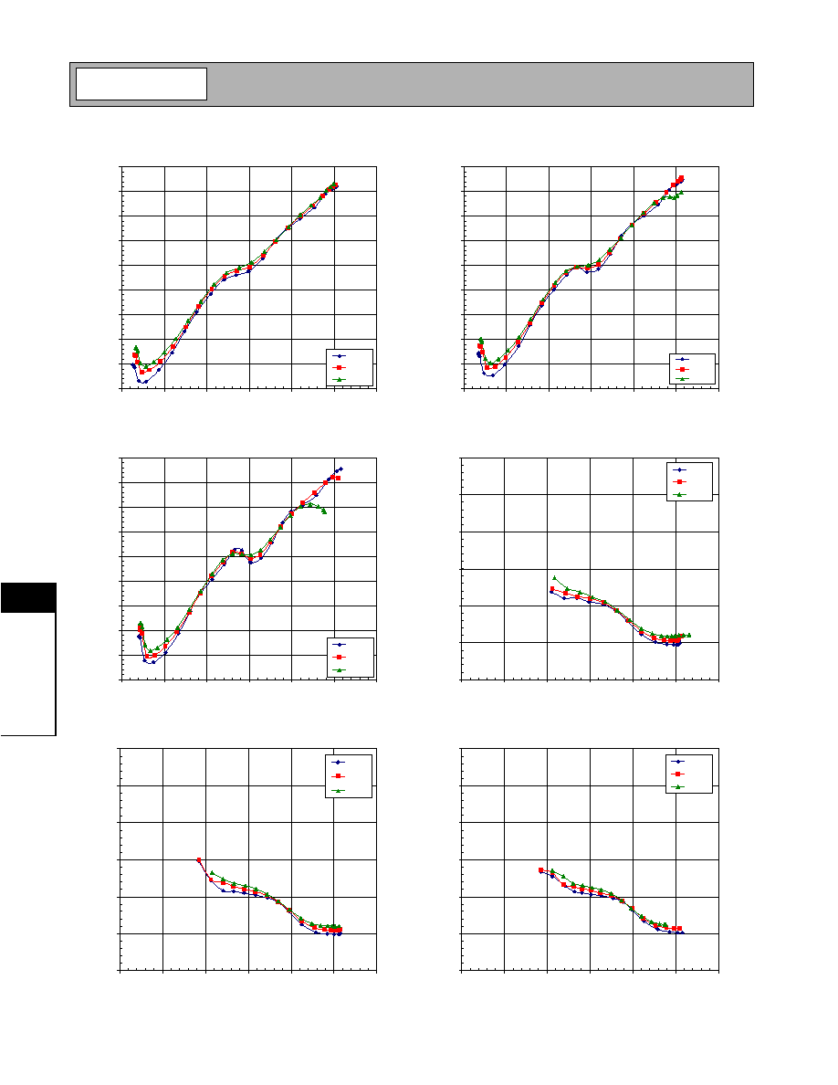
OIP3 versus Gain
(V
CC
=2.7 V, 130 MHz)
-70.0
-60.0
-50.0
-40.0
-30.0
-20.0
-10.0
0.0
10.0
20.0
-60.0
-40.0
-20.0
0.0
20.0
40.0
60.0
Gain (dB)
OIP3
(dB)
-30 C
+25 C
+80 C
OIP3 versus Gain
(V
CC
=3.0 V, 130 MHz)
-70.0
-60.0
-50.0
-40.0
-30.0
-20.0
-10.0
0.0
10.0
20.0
-60.0
-40.0
-20.0
0.0
20.0
40.0
60.0
Gain (dB)
NF
(dB)
-30 C
+25 C
+80 C
OIP3 versus Gain
(V
CC
=3.3 V, 130 MHz)
-70.0
-60.0
-50.0
-40.0
-30.0
-20.0
-10.0
0.0
10.0
20.0
-60.0
-40.0
-20.0
0.0
20.0
40.0
60.0
Gain (dB)
OIP3
(dB)
-30 C
+25 C
+ 80 C
Noise Figure versus Gain
(V
CC
=2.7 V, 130 MHz)
0.0
10.0
20.0
30.0
40.0
50.0
60.0
-60.0
-40.0
-20.0
0.0
20.0
40.0
60.0
Gain (dB)
NF
(dB)
-30 C
+25 C
+80 C
Noise Figure versus Gain
(V
CC
=3.0 V, 130 MHz)
0.0
10.0
20.0
30.0
40.0
50.0
60.0
-60.0
-40.0
-20.0
0.0
20.0
40.0
60.0
Gain (dB)
NF
(dB)
-30 C
+25 C
+80 C
Noise Figure versus Gain
(V
CC
=3.3 V, 130 MHz)
0.0
10.0
20.0
30.0
40.0
50.0
60.0
-60.0
-40.0
-20.0
0.0
20.0
40.0
60.0
Gain (dB)
NF
(dB)
-30 C
+25 C
+ 80 C