6-1
Product Description
Ordering Information
Typical Applications
Features
Functional Block Diagram
RF Micro Devices, Inc.
7628 Thorndike Road
Greensboro, NC 27409, USA
Tel (336) 664 1233
Fax (336) 664 0454
http://www.rfmd.com
Optimum Technology MatchingÆ Applied
Si BJT
GaAs MESFET
GaAs HBT
Si Bi-CMOS
!
SiGe HBT
Si CMOS
6
MI
XE
RS
GaInP/HBT
GaN HEMT
SiGe Bi-CMOS
1
2
3
4
8
7
6
5
IF-
IF+
BYP
LO-
RF OUT
VCC
GND
LO+
RF2641
CDMA UPCONVERTER/BPSK MODULATOR
∑ PCS/Cellular CDMA Systems
∑ PHS 1500/ WLAN 2400 Systems
∑ General Purpose Upconverter
∑ BPSK Modulation
∑ Micro-Cell PCS Base Stations
∑ Portable Battery-Powered Equipment
The RF2641 is a complete upconverter designed for cel-
lular and PCS applications. This device may also be used
to directly BPSK modulate a carrier. The unit operates at
3.0V and is designed as part of the RFMD PCS/Cellular
CDMA Chip Set, consisting of a Transmit IF AGC Amp,
this Transmit Upconverter, a Receive LNA/Mixer, and a
Receive IF AGC Amp.
∑ Supports Dual Mode Operation
∑ +5.5dBm Output Intercept Point
∑ 7dB Conversion Gain (836MHz)
∑ Single 3.0V Power Supply
∑ Miniature 8 Pin Package
∑ Double-Balanced Mixer
RF2641
CDMA Upconverter/BPSK Modulator
RF2641410 PCBA Fully Assembled Evaluation Board, PCS Band
RF2641411 PCBA Fully Assembled Evaluation Board, Cellular Band
6
Rev A7 020528
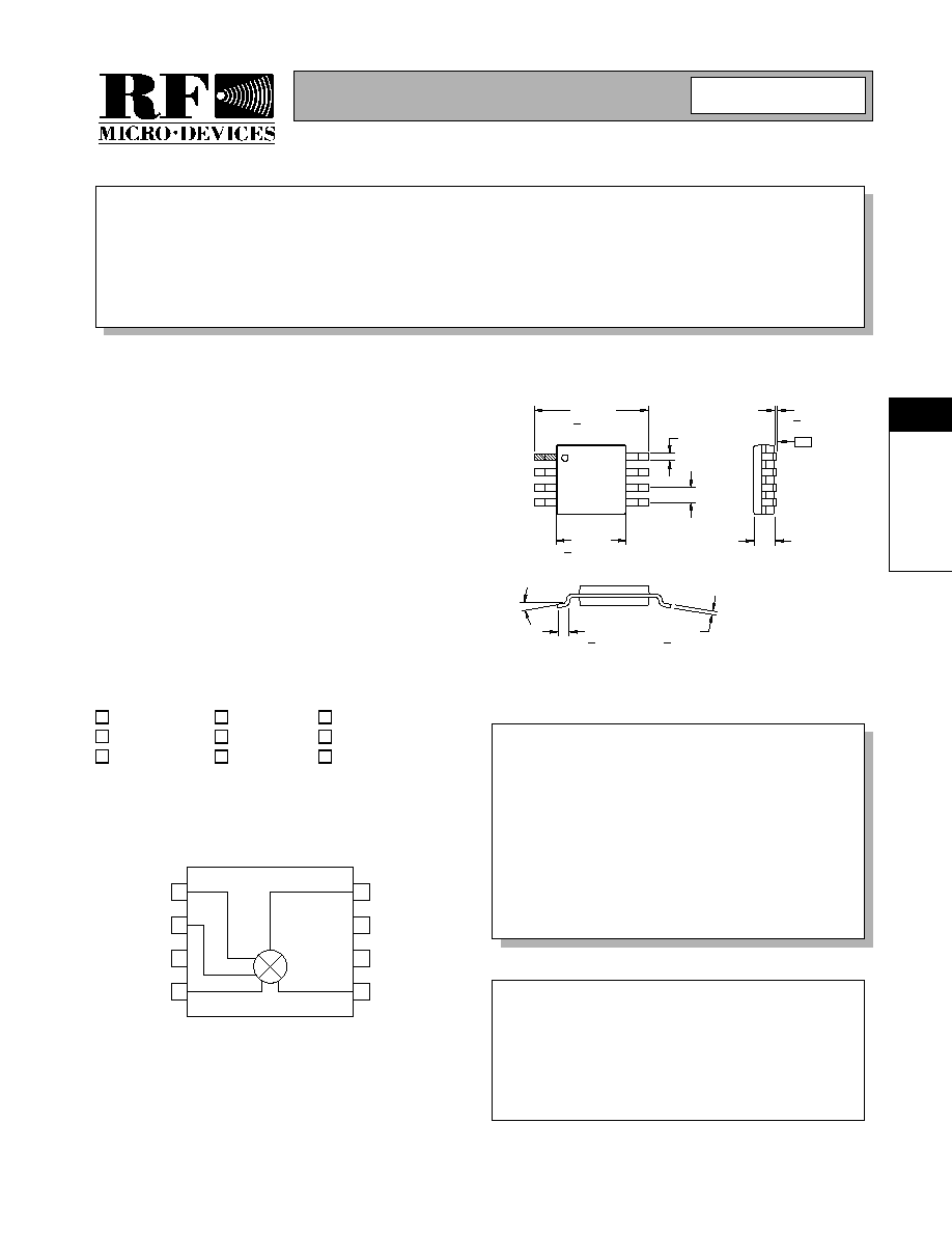
NOTES:
1. Shaded lead is pin 1.
2. All dimensions are exclusive of
flash, protrusions or burrs.
3. Lead coplanarity: 0.002 with
respect to datum "A".
0.012
6∞ MAX
0∞ MIN
0.021
+ 0.004
0.006
+ 0.002
0.192
+ 0.008
0.0256
0.118
+ 0.004 sq.
0.006
+ 0.003
0.034
-A-
Package Style: MSOP-8

6-2
RF2641
Rev A7 020528
6
MI
XE
RS
Absolute Maximum Ratings
Parameter
Rating
Unit
Supply Voltage
-0.5 to +5.0
V
DC
Input RF Power
+3
dBm
Operating Ambient Temperature
-30 to +80
∞C
Storage Temperature
-30 to +150
∞C
Parameter
Specification
Unit
Condition
Min.
Typ.
Max.
Overall
T=25∞C, V
CC
=3.0V, IF=130MHz
RF Output Frequency Range
500 to 2500
MHz
Conversion Gain
5
7
dB
RF out=836MHz, LO=-3dBm@960MHz
4
dB
RF out=1880MHz, LO=-3dBm@2010MHz
Noise Figure
10
dB
RF out=836MHz
11
dB
RF out=1880MHz
Output IP3
+3
+5.5
dBm
P
IN
=-18dBm per Tone, RF out=836MHz
+4
P
IN
=-18dBm per Tone, RF out=1880MHz
Spurious Product Rejection
30
dBc
Referenced to RF output
IF Input
IF Frequency
DC to 300
MHz
Differential Input Impedance
260
IF to RF Output Isolation
30
dB
IF to LO Isolation
30
dB
LO Input
LO Frequency Range
300 to 2700
MHz
LO Level
-6 to 0
dBm
LO to RF Output Leakage
-15
-20
dBm
RF to LO Isolation
30
dB
LO Input VSWR
2:1
50
Power Supply
Voltage
2.7 to 3.3
V
Current Consumption
13
16
mA
Caution! ESD sensitive device.
RF Micro Devices believes the furnished information is correct and accurate
at the time of this printing. However, RF Micro Devices reserves the right to
make changes to its products without notice. RF Micro Devices does not
assume responsibility for the use of the described product(s).

6-3
RF2641
Rev A7 020528
6
MI
XE
RS
Pin
Function
Description
Interface Schematic
1
IF-
Balanced IF input pin. This pin is internally DC-biased and should be
DC-blocked if connected to a device with a DC level present. For single-
ended input operation, one pin is used as an input and the other IF
input is AC-coupled to ground. The balanced, as well as single-ended,
input impedance is 260
.
2
IF+
Same as pin 1, except complementary input.
See Pin 1.
3
BYP
Bypass pin for internal bias circuitry. Bypass with a 1nF capacitor.
4
LO-
Balanced LO input pin. This pin is internally DC-biased and should be
DC-blocked if connected to a device with a DC level present. For single-
ended input operation, one pin is used as an input and the other LO
input is AC-coupled to ground. The balanced, as well as single-ended,
input impedance is 50
.
5
LO+
Same as pin 4, except complementary input.
See Pin 4.
6
GND
Ground connection. For best performance, keep traces physically short
and connect immediately to ground plane.
7
VCC
Supply voltage pin. External bypassing is required. External RF, LO,
and IF bypassing is required. The trace length between the pin and the
bypass capacitors should be minimized. The ground side of the bypass
capacitors should connect immediately to ground plane.
8
RF OUT
RF output pin.
IF+
IF-
130
130
BIAS
BYP
LO+
LO-
BIAS
300
RF OUT

6-4
RF2641
Rev A7 020528
6
MI
XE
RS
Application Schematic
836MHz
Application Schematic
1880MHz
RF OUT
IF-
IF+
LO
V
CC
1
2
3
4
8
7
6
5
12 nH
V
CC
1 nF
1 nF
1 nF
1 nF
10 nF
2 pF
10 nF
1 nF
RF OUT
IF-
IF+
LO
V
CC
1
2
3
4
8
7
6
5
2.7 nH
V
CC
1 nF
1 nF
1 nF
12 pF
10 nF
1.5 pF
10 nF
12 pF

6-5
RF2641
Rev A7 020528
6
MI
XE
RS
Evaluation Board Schematic
PCS Board, IF=130MHz
(Download Bill of Materials from www.rfmd.com.)
Evaluation Board Schematic
Cellular Board, IF=130MHz
1
2
3
4
8
7
6
5
C6
1.5 pF
50
µ
strip
J3
RF OUT
L2
2.7 nH
VCC
C7
10 nF
C1
10 nF
C4
12 pF
C3
12 pF
50
µ
strip
J1
LO
C2
1 nF
T1
T4-1
L1
270 nH
C5
68 pF
50
µ
strip
J2
IF IN
2641400, R-
P1-1
P1
1
2
3
VCC
GND
1
2
3
4
8
7
6
5
C6
2 pF
50
µ
strip
J3
RF OUT
L2
12 nH
VCC
C7
10 nF
C1
10 nF
C4
1 nF
C3
1 nF
50
µ
strip
J1
LO
C2
1 nF
T1
T4-1
L1
270 nH
C5
68 pF
50
µ
strip
J2
IF IN
2641401A
P1-1
P1
1
2
3
VCC
GND

6-6
RF2641
Rev A7 020528
6
MI
XE
RS
Evaluation Board Layout
Board Thickness 0.014"; Board Material FR-4