 | –≠–ª–µ–∫—Ç—Ä–æ–Ω–Ω—ã–π –∫–æ–º–ø–æ–Ω–µ–Ω—Ç: RF2643 | –°–∫–∞—á–∞—Ç—å:  PDF PDF  ZIP ZIP |

6-37
6
MI
X
E
R
S
Preliminary
Product Description
Ordering Information
Typical Applications
Features
Functional Block Diagram
RF Micro Devices, Inc.
7628 Thorndike Road
Greensboro, NC 27409, USA
Tel (336) 664 1233
Fax (336) 664 0454
http://www.rfmd.com
Optimum Technology MatchingÆ Applied
Si BJT
GaAs MESFET
GaAs HBT
Si Bi-CMOS
¸
SiGe HBT
Si CMOS
19
SEL
18
CEL
L
VCC
17
CEL
L
GND
16
CEL
L
I
N
14
CELL OUT
13
VGC
12
PCS OUT
10
PCS
I
N
PCS
V
CC
9
8
VCC
7
VCC
M
I
X
5
IF-
4
IF+
3
BYPASS
2
LO
1
PD
Logic
Bi
as
C
i
r
c
ui
t
*
*
*
*
*
Represents "GND".
20
CEL
L
MI
XOUT
PCS
MI
XOUT
6
11
PCS
ATT GND
15
CELL
ATT GND
RF2643
3V DUAL-BAND UPCONVERTER
AND DRIVER AMPLIFIER
∑ TDMA/AMPS Cellular Systems
∑ CDMA/AMPS Cellular Systems
∑ PCS Systems
∑ Portable Battery-Powered Equipment
The RF2643 is a complete upconverter, dual-power
amplifier driver and attenuator designed for Cellular and
PCS systems. It is designed to upconverter and amplifies
RF signals while providing 22dB of linear gain control
range. It features digital control for the mixer and drivers.
The device features balanced IF inputs, single-ended LO
input and dual RF output for Cellular and PCS Systems
respectively. The IC is manufactured on an advanced Sili-
con Bi-CMOS process and packaged in a 20-pin,
4 mmx4mm, leadless chip carrier with an exposed die
flag.
∑ Single Supply 3.0V Operation
∑ Power Down Control
∑ Gain Control Range of 22dB
∑ Driver Amplifier Select Pin (RF Output
Select)
∑ High Linearity in Mixer and Driver Amp
RF2643
3V Dual-Band Upconverter and Driver Amplifier
RF2643 PCBA
Fully Assembled Evaluation Board
6
Rev A1 010717
1.00
0.90
4.00
sq.
0.60
0.24 typ
3
0.20
0.75
0.50
0.23
0.13
4 PLCS
0.50
2.10
sq.
0.65
0.30
4 PLCS
0.05
12∞
MAX
Dimensions in mm.
Note orientation of package.
NOTES:
Package Warpage: 0.05 mm max.
4
Die Thickness Allowable: 0.305 mm max.
5
Pin 1 identifier must exist on top surface of package by identification
mark or feature on the package body. Exact shape and size is optional.
2
Shaded lead is Pin 1.
1
Dimension applies to plated terminal: to be measured between 0.02 mm
and 0.25 mm from terminal end.
3
Package Style: LCC, 20-Pin, 4x4

Preliminary
6-38
RF2643
Rev A1 010717
6
MI
X
E
R
S
Absolute Maximum Ratings
Parameter
Rating
Unit
Supply Voltage
-0.5 to +3.6
V
DC
Input RF Power
+3
dBm
Operating Ambient Temperature
-30 to +80
∞C
Storage Temperature
-30 to +150
∞C
Parameter
Specification
Unit
Condition
Min.
Typ.
Max.
Upconverter
Both Bands
Unless stated otherwise, all data in this sec-
tion is for both Cellular and PCS bands.
T = 25∞C, V
CC
= 2.75V.
IF Frequency Range
100
250
MHz
LO Input Level
-9
-6
-2
dBm
RF to LO Isolation
20
30
dBm
IF to RF Isolation
40
dBm
IF to LO Isolation
34
dBm
IF Input Impedance Differential
260
IF Input Return Loss Differential
10
dB
LO Input Impedance
Single-Ended
50
LO Input Return Loss
Single-Ended
10
dB
RF Output Impedance
Single-Ended
50
RF Output Return Loss
Single-Ended
10
dB
Cellular Band
RF= 835MHz, LO= 990MHz @-3dBm
RF Output Frequency
824
849
MHz
LO Frequency Range
909
1099
MHz
IF-RF Conversion Gain
-2
0
2
dB
Noise Figure
12
13
dB
Room Temp.
13
14
Over Temp.
Output IP3 (Linearity)
10.5
13.0
dBm
See Note 1 (end of parameter table).
Output P1dB
-3
-1
dBm
LO to RF Output Leakage
-30
dBm
PCS Band
RF= 1880MHz, LO =2030MHz@-3dBm
RF Output Frequency
1850
1910
MHz
LO Frequency Range
1950
2160
MHz
IF-RF Conversion Gain
-2
0
2
dB
Noise Figure
14.0
14.5
dB
Room Temp.
15.0
16.5
Over Temp.
Output IP3 (Linearity)
8.5
12.0
dBm
See Note 1 (end of parameter table).
Output P1dB
-4
-2
dBm
LO to RF Output Leakage
-17
dBm
Caution! ESD sensitive device.
RF Micro Devices believes the furnished information is correct and accurate
at the time of this printing. However, RF Micro Devices reserves the right to
make changes to its products without notice. RF Micro Devices does not
assume responsibility for the use of the described product(s).

Preliminary
6-39
RF2643
Rev A1 010717
6
MI
X
E
R
S
NOTE 1: OIP3 was measured using a two-tone test. Each injected tone had an input power (at the RF output of the
upconverter) of -18 dBm with a frequency spacing of 100 kHz.
Parameter
Specification
Unit
Condition
Min.
Typ.
Max.
Amplifiers/Attenuators
Both Bands
Unless stated otherwise, all data in this sec-
tion is for both Cellular and PCS bands.
T= 25∞C, V
CC
=2.75V.
Gain Control Range
17
20
dB
Gain Control Voltage
0.8
1.9
V
Gain Control Slope
15
35
dB/V
Input Impedance
Single-Ended
50
Input Return Loss
Single-Ended
10
dB
Output Impedance
Single-Ended
50
Output Return Loss
Single-Ended
10
dB
RF Output Collector Current
Consumption
10
mA
Upconverter Output to
Amplifier Input
35
40
dB
Any load.
Cellular Band
RF Frequency Range
824
849
MHz
Maximum Gain
5
7
9
dB
Amplifier + Attenuator
Noise Figure at Maximum Gain
2.5
dB
Amplifier + Attenuator
Noise Figure Increase with
Attenuation
0.75
dB/dB
Input IP3 (Linearity)
-1
1
dBm
@ all gain levels
See Note 1 (end of parameter table).
PCS Band
RF Frequency Range
1850
1910
MHz
Maximum Gain
4
6
8
dB
Amplifier + Attenuator
Noise Figure at Maximum Gain
3.5
dB
Amplifier + Attenuator
Noise Figure Increase with
Attenuation
0.75
dB/dB
Input IP3 (Linearity)
-1
0
dBm
See Cellular Band Input IP3 Conditions.
Control and Power
Consumption
Unless otherwise stated, all data in this sec-
tion is for both Cellular and PCS bands.
Operating Voltage
2.7
3.0
V
Power Down Control
2.1
V
HIGH (Device ON)
0.5
V
LOW (Device OFF)
Power Down Pin Impedance
20
k
Band-Select Control (BS)
2.1
V
PCS (HIGH)
0.5
V
Cellular (LOW)
Band Select Pin Impedance
20
k
Device OFF Current
10
uA
PD = LOW
Total Current (PD = HIGH)
30
37
mA
Cellular, BS =LOW
33
42
mA
PCS, BS= HIGH
Preliminary
6-40
RF2643
Rev A1 010717
6
MI
X
E
R
S
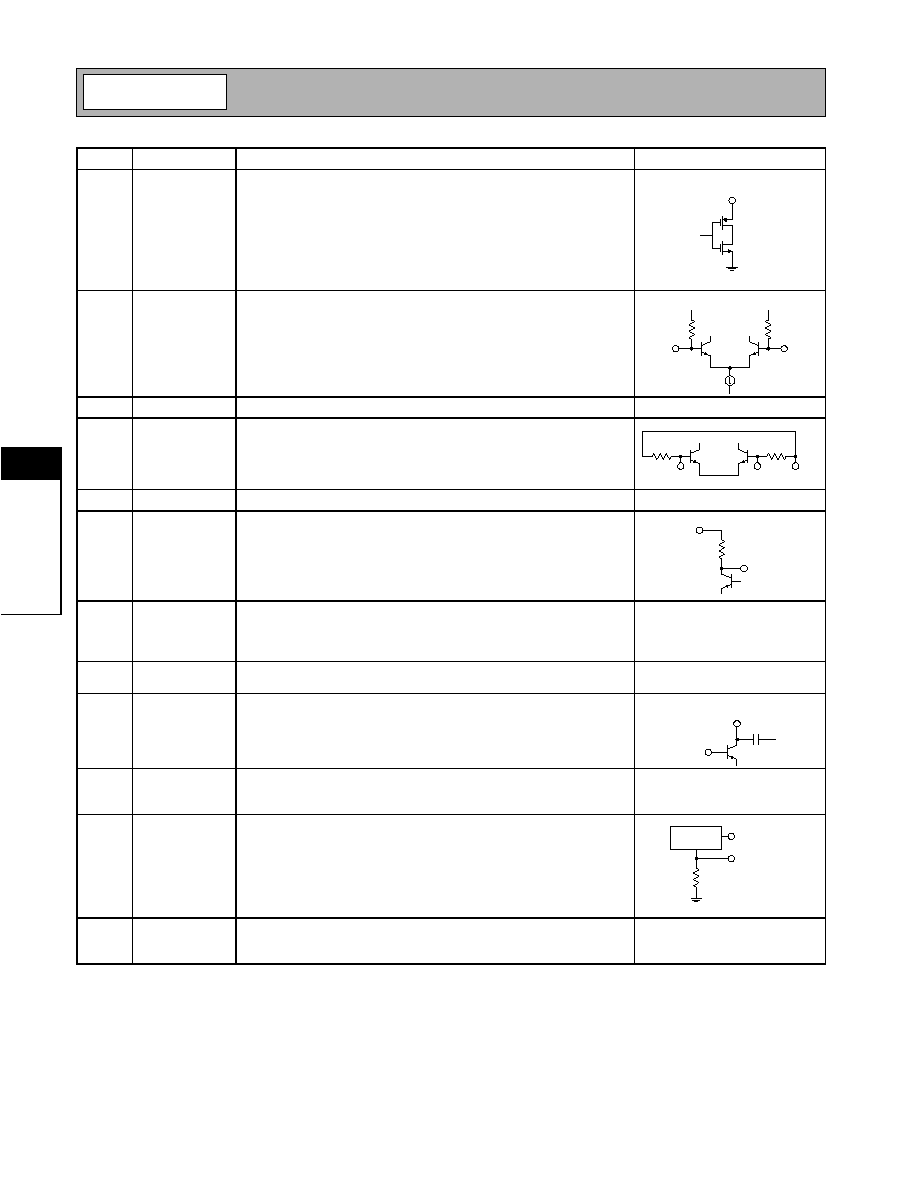
Pin
Function
Description
Interface Schematic
1
PD
Power Down Control. When Logic "high" (greater than 2.1V) the device
is active and all circuits are operating. When logic "low" (less than 0.5V)
the device is inactive and all circuits are turned off.
2
LO
Single-ended LO input pin. This pin is internally DC biased and should
be DC blocked if it is connected to a device with a DC level present.
The single-ended input impedance is 50
.
3
BYPASS
Bypass pin for internal bias circuitry. Bypass with 10nF capacitor.
4
IF+
Balanced IF input pin. This pin is internally DC biased and should be
DC blocked if connected to a device with a DC level present. The differ-
ential input impedance is 260
. For single ended input operation, one
pin is used as an input and the other IF input is AC coupled to ground.
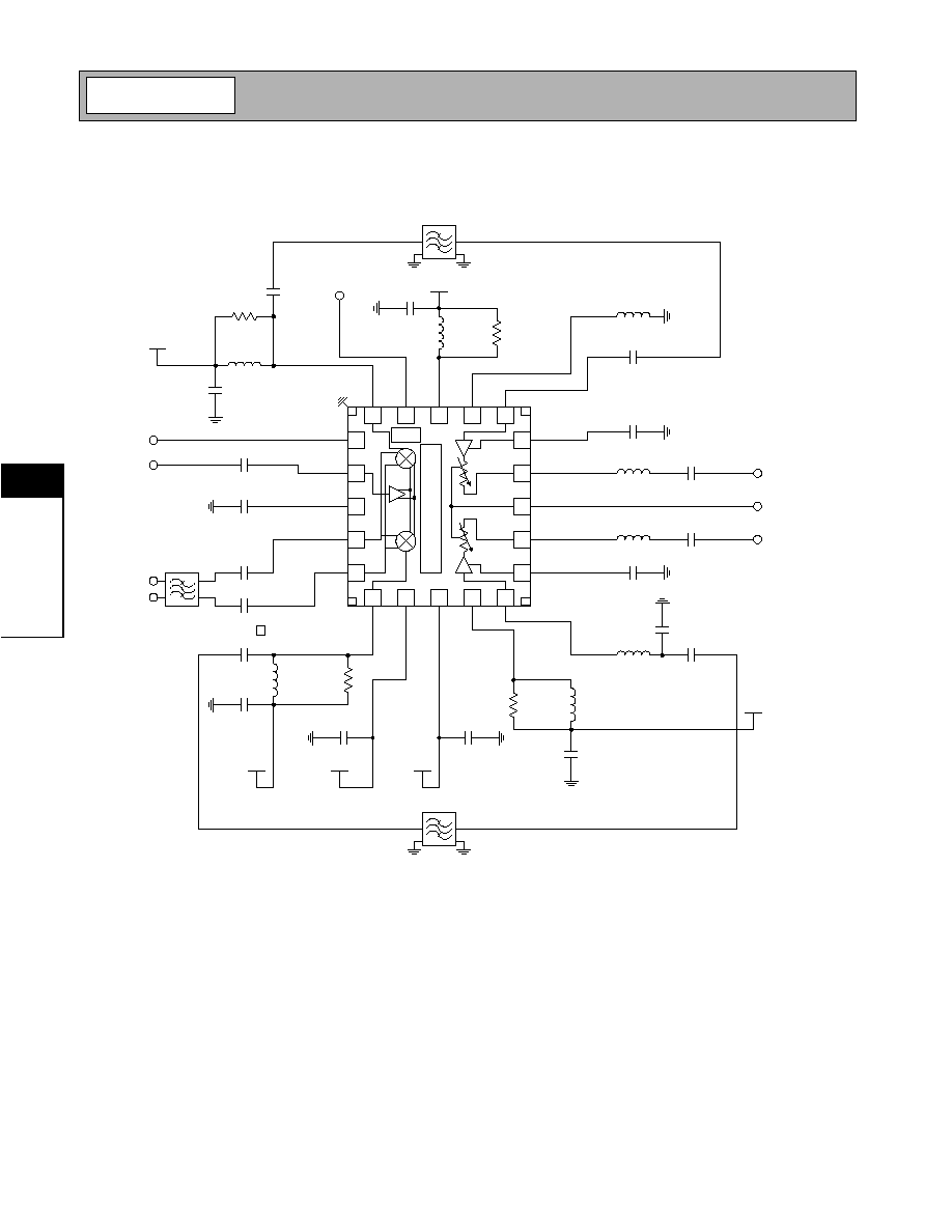
5
IF-
Same as pin 4, except complementary input.
6
PCS
MIXOUT
RF mixer output pin for the PCS system. PCS Mixout output imped-
ance depends on the LC match and it is influenced by the bypass
capacitor at VCC2.
7
VCC MIX
Supply voltage pin for the mixer. External bypassing is required. The
trace length between the pin and the bypass capacitors should be min-
imized. The ground side of the bypass capacitors should connect
immediately to ground plane.
8
VCC
Supply voltage pin for all the control and bias circuitry. A bias choke
inductor and RF bypass capacitor is required.
9
PCS VCC
Supply voltage pin for the PCS driver. This pin is an open collector and
it will need a bias choke inductor and RF bypass. A parallel resistor to
the inductor improves stability of the driver amplifier.
10
PCS IN
Single-ended input for the PCS driver and attenuator. External match-
ing is required. This pin is internally DC biased and should be DC
blocked if it is connected to a device with a DC level present.
11
PCS
ATT GND
PCS attenuator ground pin. This pin should be AC ground. The trace
length between the pin and the bypass capacitors should be minimized.
The value of the capacitor is chosen to resonate in the PCS band.
12
PCS OUT
PCS RF output pin. External matching is required. This pin is internally
DC biased and should be DC blocked if it is connected to a device with
a DC level present.
VCC
Bias
LO+
Bias
LO-
IF+
IF-
Bypass
VCC MIX
PCS MIXOUT
PCS VCC
PCS IN
PCS ATT-GND
PCS
Attenuator
PCS OUT

Preliminary
6-41
RF2643
Rev A1 010717
6
MI
X
E
R
S
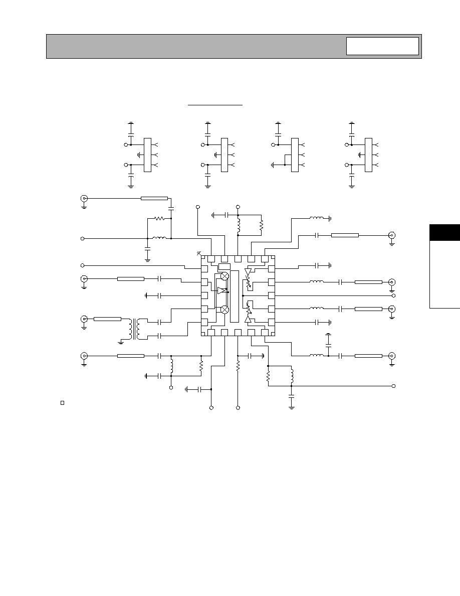
Pin
Function
Description
Interface Schematic
13
VGC
Analog gain control for the driver amplifier. Valid control voltage ranges
from 0.8V
DC
to 1.9V
DC
.
14
CELL OUT
Cellular RF output pin. External matching is required. External match-
ing is required. This pin is internally DC biased and should be DC
blocked if it is connected to a device with a DC level present.
15
CELL
ATT GND
Cell attenuator ground pin. This pin should be AC ground. The trace
length between the pin and the bypass capacitors should be minimized.
The value of the capacitor is chosen to resonate in the PCS band.
16
CELL IN
Singled end input for the cellular driver and attenuator. External match-
ing is required. This pin is internally DC biased and should be DC
blocked if it is connected to a device with a DC level present.
17
CELL GND
This pin should be choke to ground. The inductor is used to adjust the
linearity of the cellular driver.
18
CELL VCC
Supply voltage pin for the cell driver. This pin is an open collector and it
will need a bias choke inductor and RF bypass. A parallel resistor to the
inductor improves stability of the driver amplifier.
19
SEL
Band select control pin for the drivers. When Logic "high" (greater than
2.1V) the PCS band is active. When logic "low" (less than 0.5V) the
Cellular Band is active.
20
CELL
MIXOUT
RF mixer output pin for the PCS system. PCS Mixout output imped-
ance depends on the LC match and it is influenced by the bypass
capacitor at VCC2.
Pkg
Base
GND
Ground connection. The backside of the package should be soldered to
a top side ground pad, which is connected to the ground plane. Addi-
tional ground connections are offered at each corner of the package for
flexibility in layout design.
VGC
CELL ATT-GND
Cell
Attenuator
CELL OUT
CELL VCC
CELL GND
SEL
VCC MIX
CELL MIXOUT
Preliminary
6-42
RF2643
Rev A1 010717
6
MI
X
E
R
S
Application Schematic
*
Represents "GND".
19
18
17
16
14
13
12
10
9
8
7
5
4
3
2
1
Logic
B
i
as
C
i
r
c
ui
t
*
*
*
*
20
6
11
15
Die
Flag
PD
100 pF
10 nF
C*
C*
13 pF
3.3 nH
1 nF
VGC
4.7 nH
1 nF
3 pF
3 pF
3.9 nH
CC
10 nF
33 nF
2.2 nH
0.5 pF
0.1 uF
R*
240
10 nH
10 nF
12 nH
R*
390
2 pF
10 nF
SEL
0.1 uF
1.5 nH
R*
91
15 nH
10 nF
Cell RF Filter
V
CC1
V
CC2
V
CC
MIX
V
CC
V
CC2
V
CC1
R*
NOTES:
1. All components marked with "R*" are De-Q resistors.
2. All components marked with "C*" should be present, if IF SAW filter has a direct path to ground.
CELL OUT
PCS RF Filter
LO
IF Filter
IF+
IF-
33 nF
PCS OUT
Preliminary
6-43
RF2643
Rev A1 010717
6
MI
X
E
R
S
Evaluation Board Schematic
IF=155MHz
(Download Bill of Materials from www.rfmd.com.)
*
Represents "GND".
19
18
17
16
14
13
12
10
9
8
7
5
4
3
2
1
Logic
B
i
as
Ci
rc
ui
t
*
*
*
*
20
6
11
15
Die
Flag
PD
C1
100 pF
50
µ
strip
J1
LO
C2
10 nF
C3
10 nF
T1
C4
10 nF
50
µ
strip
J3
PCS MIXOUT
C12
13 pF
L5
3.3 nH
C13
1 nF
50
µ
strip
J6
CELL OUT
VGC
L4
4.7 nH
C11
1 nF
50
µ
strip
J5
PCS OUT
C10
3 pF
C6
3 pF
50
µ
strip
R4
DNI
L2
3.9 nH
CC
VCC2
C7
10 nF
VCC MIX
C25
33 nF
L8
2.2 nH
C27
0.5 pF
C9
0.1 uF
50
µ
strip
J4
PCS IN
R2
240
L3
10 nH
C8
10 nF
VCC1
C26
33 nF
R3
0
VCC
L1
12 nH
R5
390
C15
2 pF
50
µ
strip
J8
CELL MIXOUT
C17
10 nF
VCC2
SEL
J2
IF
C14
0.1 uF
50
µ
strip
J7
CELL IN
L6
1.5 nH
R1
91
L7
15 nH
VCC1
C16
10 nF
2643400-
P1
1
2
3
CON3
GND
P1-3
VCC MIX
C19
1 uF
+
P1-1
VCC
C18
1 uF
+
P2
1
2
3
CON3
SEL
P2-3
C21
33 nF
GND
PD
P2-1
C20
33 nF
P3
1
2
3
CON3
P3-1
C24
DNI
VGC
GND
GND
P4
1
2
3
CON3
GND
VCC2
P4-3
C23
1 uF
+
VCC1
P4-1
C22
1 uF
+
Preliminary
6-44
RF2643
Rev A1 010717
6
MI
X
E
R
S
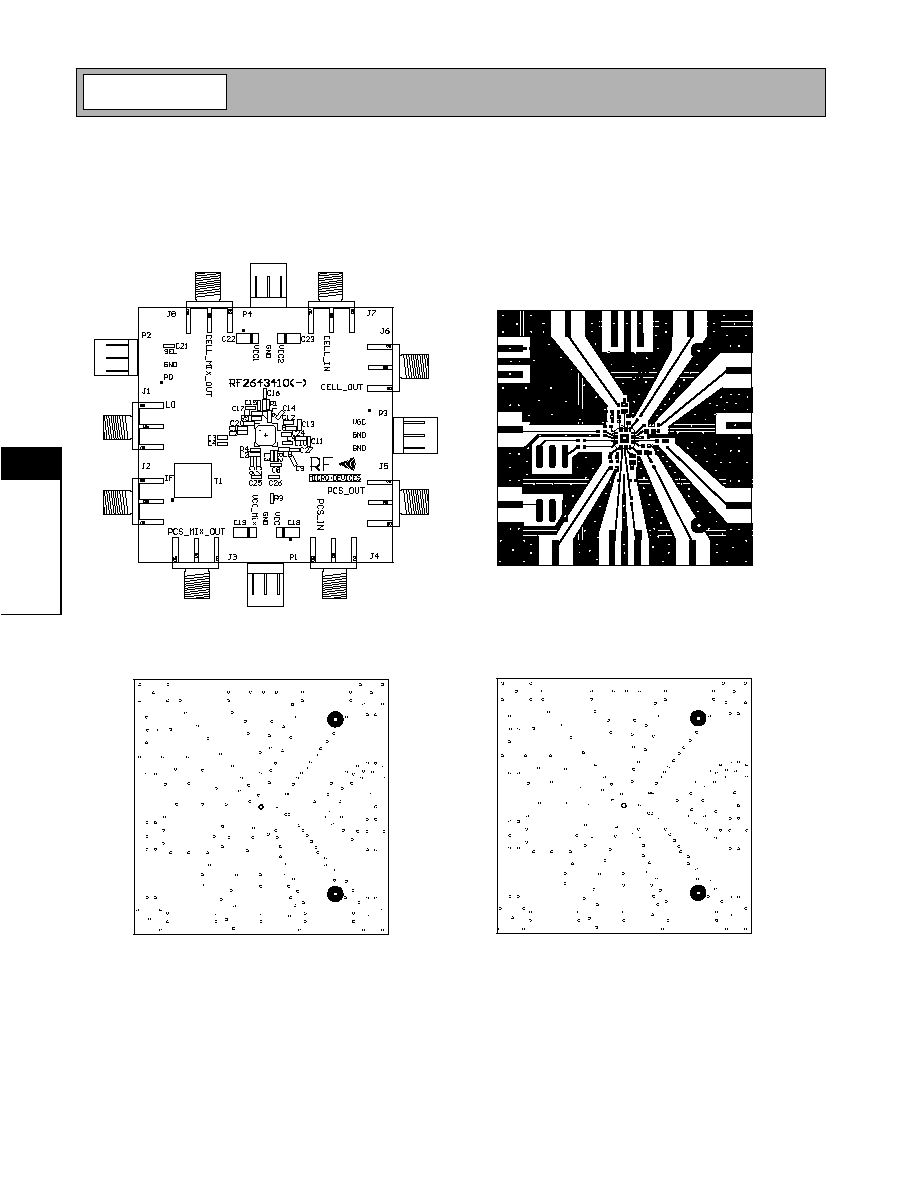
Evaluation Board Layout
Board Size 2.0" x 2.0"
Board Thickness 0.064", Board Material FR-4, Multi-Layer
Assembly
Top
Inner 1 - Ground Plane 1
Inner 2 - Power Plane 1

Preliminary
6-45
RF2643
Rev A1 010717
6
MI
X
E
R
S
Inner 3 - Ground Plane 2
Inner 4 - Power Plane 2
Back
Preliminary
6-46
RF2643
Rev A1 010717
6
MI
X
E
R
S
Power Down Current
0.0
0.2
0.4
0.6
0.8
1.0
1.2
1.4
2.7
2.8
2.9
3.0
3.1
3.2
3.3
V
CC
(V)
I
CC
(uA)
Icc, -30∫
Icc, 25∫
Icc, 85∫
Cellular Current
30.0
30.2
30.4
30.6
30.8
31.0
31.2
31.4
31.6
31.8
32.0
2.7
2.8
2.9
3.0
3.1
3.2
3.3
V
CC
(V)
Current
(mA)
Icc, -30∫
Icc, 25∫
Icc, 85∫
Cellular Mixer Conversion Gain
@ LO = -10 dBm
-2.0
-1.5
-1.0
-0.5
0.0
0.5
1.0
1.5
2.7
2.8
2.9
3.0
3.1
3.2
3.3
V
CC
(V)
Conversion
Gain
(dB)
Gain, -30∫
Gain, 25∫
Gain, 85∫
Cellular Mixer Conversion Gain
@ LO = -3 dBm
-1.5
-1.0
-0.5
0.0
0.5
1.0
1.5
2.7
2.8
2.9
3.0
3.1
3.2
3.3
V
CC
(V)
Conversion
Gain
(dB)
Gain, -30∫
Gain, 25∫
Gain, 85∫
Cellular LO to RF Leakage
@ LO = -10 dBm
-38.0
-37.5
-37.0
-36.5
-36.0
-35.5
-35.0
-34.5
-34.0
-33.5
-33.0
-32.5
2.7
2.8
2.9
3.0
3.1
3.2
3.3
V
CC
(V)
LO
to
RF
Leakage
(dBm)
LO2RF, -30∫
LO2RF, 25∫
LO2RF, 85∫
Cellular LO to RF Leakage
@ LO = -3 dBm
-28.6
-28.4
-28.2
-28.0
-27.8
-27.6
-27.4
-27.2
-27.0
-26.8
-26.6
2.7
2.8
2.9
3.0
3.1
3.2
3.3
V
CC
(V)
LO
to
RF
Leakage
(dBm)
LO2RF, -30∫
LO2RF, 25∫
LO2RF, 85∫
Preliminary
6-47
RF2643
Rev A1 010717
6
MI
X
E
R
S
Cellular Mixer OIP3
@ LO = -10 dBm
10.0
10.5
11.0
11.5
12.0
12.5
13.0
13.5
14.0
14.5
2.7
2.8
2.9
3.0
3.1
3.2
3.3
V
CC
(V)
OIP3
(dBm)
OIP3, -30∫
OIP3, 25∫
OIP3, 85∫
Cellular Mixer OIP3
@ LO = -3 dBm
10.0
10.5
11.0
11.5
12.0
12.5
13.0
13.5
14.0
14.5
2.7
2.8
2.9
3.0
3.1
3.2
3.3
V
CC
(V)
OIP3
(dBm)
OIP3, -30∫
OIP3, 25∫
OIP3, 85∫
Cellular Mixer Noise Figure
@ LO = -10 dBm
10.0
10.5
11.0
11.5
12.0
12.5
13.0
13.5
14.0
2.7
2.8
2.9
3.0
3.1
3.2
3.3
V
CC
(V)
Noise
Figure
(
dB)
NF, -30∫
NF, 25∫
NF, 85∫
Cellular Mixer Noise Figure
@ LO = -3 dBm
10.0
10.5
11.0
11.5
12.0
12.5
13.0
2.7
2.8
2.9
3.0
3.1
3.2
3.3
V
CC
(V)
Noise
Figure
(
dB)
NF, -30∫
NF, 25∫
NF, 85∫
Cellular Mixer Gain
@ 25∞C
-4.0
-3.5
-3.0
-2.5
-2.0
-1.5
-1.0
-0.5
0.0
0.5
-10.0
-9.0
-8.0
-7.0
-6.0
-5.0
-4.0
-3.0
-2.0
V
CC
(V)
Conversion
Gain
(dB)
2.7 V
3 V
3.3 V
Cellular Mixer OIP3
@ 25∞C
10.0
10.5
11.0
11.5
12.0
12.5
13.0
13.5
14.0
-10.0
-9.0
-8.0
-7.0
-6.0
-5.0
-4.0
-3.0
-2.0
LO (dBm)
OIP3
(dBm)
2.7 V
3 V
3.3 V

Preliminary
6-48
RF2643
Rev A1 010717
6
MI
X
E
R
S
Cellular Mixer Noise Figure
@ 25∞C
11.6
11.7
11.8
11.9
12.0
12.1
12.2
-10.0
-9.0
-8.0
-7.0
-6.0
-5.0
-4.0
-3.0
-2.0
LO (dBm)
Noise
Figure
(
dB)
2.7 V
3 V
3.3 V
Cellular Gain Driver
@ 25∞C
-20.0
-15.0
-10.0
-5.0
0.0
5.0
10.0
0.7
0.9
1.1
1.3
1.5
1.7
1.9
V
GC
(V)
Gain
(dB)
2.7 V
3 V
3.3 V
Cellular Driver IIP3
@ 25∞C
0.0
1.0
2.0
3.0
4.0
5.0
6.0
7.0
8.0
9.0
0.7
0.9
1.1
1.3
1.5
1.7
1.9
2.1
V
GC
(V)
IIP3
(dBm)
2.7 V
3 V
3.3 V
Cellular Noise Figure Driver
@ 25∞C
0.0
2.0
4.0
6.0
8.0
10.0
12.0
14.0
16.0
18.0
0.7
0.9
1.1
1.3
1.5
1.7
1.9
2.1
V
GC
(V)
Noise
Figure
(
dB)
2.7 V
3 V
3.3 V
Cellular Gain Driver
@ 2.7 V
-20.0
-15.0
-10.0
-5.0
0.0
5.0
10.0
0.5
1.0
1.5
2.0
V
GC
(V)
Gain
(dB)
Gain, -30∫
Gain, 25∫
Gain, 85∫
Cellular Driver IIP3
@ 2.7 V
0.0
1.0
2.0
3.0
4.0
5.0
6.0
7.0
8.0
9.0
0.7
0.9
1.1
1.3
1.5
1.7
1.9
2.1
V
GC
(V)
IIP3
(dBm)
IIP3, -30∫
IIP3, 25∫
IIP3, 85∫

Preliminary
6-49
RF2643
Rev A1 010717
6
MI
X
E
R
S
Cellular Driver Noise Figure
@ 2.7 V
0.0
2.0
4.0
6.0
8.0
10.0
12.0
14.0
16.0
18.0
0.7
0.9
1.1
1.3
1.5
1.7
1.9
2.1
V
GC
(V)
Noise
Figure
(
dB)
NF, -30∫
NF, 25∫
NF, 85∫
PCS Current
31.5
31.7
31.9
32.1
32.3
32.5
32.7
32.9
33.1
33.3
33.5
2.7
2.8
2.9
3.0
3.1
3.2
3.3
V
CC
(V)
Current
(mA)
Icc, -30∫
Icc, 25∫
Icc, 85∫
PCS Mixer Conversion Gain
@ LO = -10 dBm
-2.5
-2.0
-1.5
-1.0
-0.5
0.0
0.5
1.0
1.5
2.7
2.8
2.9
3.0
3.1
3.2
3.3
V
CC
(V)
Conversion
Gain
(dB)
Gain, -30∫
Gain, 25∫
Gain, 85∫
PCS Mixer Conversion
@ LO = -3 dBm
-2.0
-1.5
-1.0
-0.5
0.0
0.5
1.0
1.5
2.7
2.8
2.9
3.0
3.1
3.2
3.3
V
CC
(V)
Conversion
Gain
(dB)
Gain, -30∫
Gain, 25∫
Gain, 85∫
PCS LO to RF Leakage
@ LO = -10 dBm
-22.4
-22.3
-22.2
-22.1
-22.0
-21.9
-21.8
-21.7
-21.6
-21.5
-21.4
-21.3
2.7
2.8
2.9
3.0
3.1
3.2
3.3
V
CC
(V)
LO
to
RF
Leakage
(dBm)
LO2RF, -30∫
LO2RF, 25∫
LO2RF, 85∫
PCS LO to RF Leakage
@ LO = -3 dBm
-18.20
-18.15
-18.10
-18.05
-18.00
-17.95
-17.90
-17.85
-17.80
-17.75
-17.70
-17.65
2.70
2.80
2.90
3.00
3.10
3.20
3.30
V
CC
(V)
LO
to
RF
Leakage
(dBm)
LO2RF, -30∫
LO2RF, 25∫
LO2RF, 85∫
Preliminary
6-50
RF2643
Rev A1 010717
6
MI
X
E
R
S
PCS Mixer OIP3
@ LO = -10 dBm
8.0
8.5
9.0
9.5
10.0
10.5
11.0
11.5
12.0
12.5
13.0
2.7
2.8
2.9
3.0
3.1
3.2
3.3
V
CC
(V)
OIP3
(dBm)
OIP3, -30∫
OIP3, 25∫
OIP3, 85∫
PCS Mixer OIP3
@ LO = -3 dBm
9.0
9.5
10.0
10.5
11.0
11.5
12.0
12.5
13.0
2.7
2.8
2.9
3.0
3.1
3.2
3.3
V
CC
(V)
OIP3
(dBm)
OIP3, -30∫
OIP3, 25∫
OIP3, 85∫
PCS Mixer Noise Figure
@ LO = -10 dBm
12.0
12.5
13.0
13.5
14.0
14.5
15.0
15.5
16.0
16.5
17.0
2.7
2.8
2.9
3.0
3.1
3.2
3.3
V
CC
(V)
Noise
Figure
(
dB)
NF, -30∫
NF, 25∫
NF, 85∫
PCS Mixer Noise Figure
@ LO = -3 dBm
12.0
12.5
13.0
13.5
14.0
14.5
15.0
2.7
2.8
2.9
3.0
3.1
3.2
3.3
V
CC
(V)
Noise
Figure
(
dB)
NF, -30∫
NF, 25∫
NF, 85∫
PCS Mixer Conversion Gain
@ 25∞C
-0.7
-0.6
-0.5
-0.4
-0.3
-0.2
-0.1
0.0
-10.0
-9.0
-8.0
-7.0
-6.0
-5.0
-4.0
-3.0
-2.0
LO (dBm)
Conversion
Gain
(dB)
2.7 V
3 V
3.3 V
PCS Mixer OIP3
@ 25∞C
11.0
11.2
11.4
11.6
11.8
12.0
12.2
12.4
12.6
-10.0
-9.0
-8.0
-7.0
-6.0
-5.0
-4.0
-3.0
-2.0
LO (dBm)
OIP3
(dBm)
2.7 V
3 V
3.3 V
Preliminary
6-51
RF2643
Rev A1 010717
6
MI
X
E
R
S
PCS Mixer Noise Figure
@ 25∞C
13.2
13.3
13.4
13.5
13.6
13.7
13.8
13.9
14.0
14.1
14.2
14.3
-10.0
-9.0
-8.0
-7.0
-6.0
-5.0
-4.0
-3.0
-2.0
LO (dBm)
Noise
Figure
(
dB)
2.7 V
3 V
3.3 V
PCS Gain Driver
@ 25∞C
-20.0
-15.0
-10.0
-5.0
0.0
5.0
10.0
0.7
0.9
1.1
1.3
1.5
1.7
1.9
2.1
V
GC
(V)
Gain
(dB)
2.7 V
3 V
3.3 V
PCS IIP3 Driver
@ 25∞C
0.0
2.0
4.0
6.0
8.0
10.0
12.0
14.0
0.7
0.9
1.1
1.3
1.5
1.7
1.9
2.1
V
GC
(V)
IIP3
(dBm)
2.7 V
3 V
3.3 V
PCS Noise Figure Driver
@ 25∞C
0.0
2.0
4.0
6.0
8.0
10.0
12.0
14.0
16.0
18.0
0.7
0.9
1.1
1.3
1.5
1.7
1.9
2.1
V
GC
(V)
Noise
Figure
(
dB)
2.7 V
3 V
3.3 V
PCS Gain Driver
@ 2.7 V
-20.0
-15.0
-10.0
-5.0
0.0
5.0
10.0
0.7
0.9
1.1
1.3
1.5
1.7
1.9
2.1
V
GC
(V)
Gain
(dB)
Gain, -30∫
Gain, 25∫
Gain, 85∫
PCS IIP3 Driver
@ 2.7 V
0.0
2.0
4.0
6.0
8.0
10.0
12.0
0.7
0.9
1.1
1.3
1.5
1.7
1.9
2.1
V
GC
(V)
IIP3
(dBm)
IIP3, -30∫
IIP3, 25∫
IIP3, 85∫
Preliminary
6-52
RF2643
Rev A1 010717
6
MI
X
E
R
S
PCS Noise Figure Driver
@ 2.7 V
0.0
2.0
4.0
6.0
8.0
10.0
12.0
14.0
16.0
18.0
0.7
0.9
1.1
1.3
1.5
1.7
1.9
2.1
V
GC
(V)
Noise
Figure
(
dB)
NF, -30∫
NF, 25∫
NF, 85∫