 | –≠–ª–µ–∫—Ç—Ä–æ–Ω–Ω—ã–π –∫–æ–º–ø–æ–Ω–µ–Ω—Ç: RF2667 | –°–∫–∞—á–∞—Ç—å:  PDF PDF  ZIP ZIP |

¸
7-1
7
Q
U
ADR
A
T
U
RE
DEM
O
DU
L
A
T
O
R
S
Product Description
Ordering Information
Typical Applications
Features
Functional Block Diagram
RF Micro Devices, Inc.
7625 Thorndike Road
Greensboro, NC 27409, USA
Tel (336) 664 1233
Fax (336) 664 0454
http://www.rfmd.com
Optimum Technology MatchingÆ Applied
Si BJT
GaAs MESFET
GaAs HBT
Si Bi-CMOS
SiGe HBT
Si CMOS
Quad.
˜
2
Input
Select
Gain
Control
Band Gap
Reference
19
4
5
8
9
CDMA IN+
CDMA IN-
FM IN+
FM IN-
BG
O
U
T
23
GC
FL
+
FL
-
10
24
PD
14
IN SEL
18
Q OUT+
I OUT+
Q OUT-
13
12
LO+
LO-
16
15
21
22 I OUT-
RF2667
RECEIVE AGC AND DEMODULATOR
∑ CDMA/FM Cellular Systems
∑ CDMA PCS Systems
∑ GSM/DCS Systems
∑ TDMA Systems
∑ Spread-Spectrum Cordless Phones
∑ Wireless Local Loop Systems
The RF2667 is an integrated complete IF AGC amplifier
and quadrature demodulator developed for the receive
section of dual-mode CDMA/FM cellular and PCS appli-
cations and for GSM/DCS and TDMA systems. It is
designed to amplify received IF signals, while providing
100dB of gain control range, and demodulate to base-
band I and Q signals. Noise figure, IP
3
, and other specifi-
cations are designed to be compatible with the IS-98, and
J-STD-018 Interim Standard for CDMA cellular communi-
cations. This circuit is part of the RFMD line of complete
solutions for digital radio applications. The IC is manufac-
tured on an advanced 15GHz F
T
Silicon Bipolar process,
and is packaged in a standard miniature 24-lead plastic
QSOP package.
∑ Similar to RF9957with Higher I/Q Output
Voltage
∑ Supports Dual Mode Operation
∑ Digitally Controlled Power Down Mode
∑ 2.7V to 3.3V Operation
∑ IF AGC Amp with 100dB Gain Control
RF2667
Receive AGC and Demodulator
RF2667 PCBA
Fully Assembled Evaluation Board
7
Rev A14 010622
NOTES:
1. Shaded lead is Pin 1.
2. All dimensions are excluding mold flash.
3. Lead coplanarity: 0.005 with respect to datum "A".
Dimensions in inches.
0.2440
0.2284
0.344
0.337
0.157
0.150
0.012
0.008
0.025
0.0098
0.0040
-A-
0.0688
0.0532
0.0098
0.0075
0.050
0.016
8∞ MAX
0∞ MIN
Package Style: QSOP-24
7-2
RF2667
Rev A14 010622
7
Q
U
ADR
A
T
U
RE
DEM
O
DU
L
A
T
O
R
S
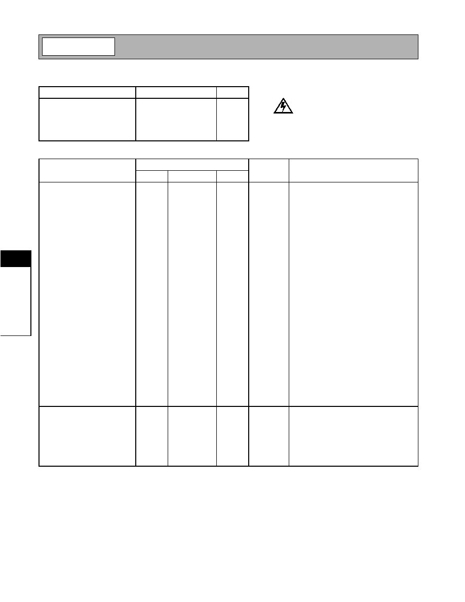
Absolute Maximum Ratings
Parameter
Rating
Unit
Supply Voltage
-0.5 to +5
V
DC
Power Down Voltage (V
PD
)
-0.5 to V
CC
+0.7
V
DC
Input RF Power
+3
dBm
Ambient Operating Temperature
-40 to +85
∞C
Storage Temperature
-40 to +150
∞C
Parameter
Specification
Unit
Condition
Min.
Typ.
Max.
Overall (Cascaded)
T = 25 ∞C, V
CC
= 3.0V, Z
LOAD
=5k
,
LO= 170MHz @400mV
PP
, IF Freq= 85MHz,
Z
S
= 500
(CDMA), Z
S
= 850
(FM)
Maximum Gain
+45
+50
dB
V
GC
= 2.5V, FM or CDMA Input, Balanced
Minimum Gain
-55
-50
dB
V
GC
= 0.5V, FM or CDMA Input, Balanced
Gain Variation
-3
+3
dB
T = -20∞C to +85∞C, Ref = 25∞C
Input IP3
-54
-50
dBm
V
GC
= 2.5V, Maximum Gain
-7
-4
dBm
V
GC
= 0.5V, Minimum Gain
-39
-36
dBm
Gain = 35 dB, P
IN
=-61dBm
Noise Figure
5
8
dB
V
GC
= 2.5V, Maximum Gain
70
77
dB
V
GC
= 0.5V, Minimum Gain
IF Input Frequency Range
50
70 to 230
250
MHz
IF Input Impedance
2040
2400
2760
FM or CDMA, Balanced
1020
1200
1380
FM or CDMA, Single-ended
I/Q Frequency Range
0
50
MHz
I/Q Amplitude Balance
0.1
0.5
dB
I/Q Phase Balance
1
5
deg
Max I/Q Output Voltage
2.0
2.4
V
PP
Balanced, maximum output level
I/Q Output Impedance
1020
1200
1380
Single-ended
2040
2400
2760
Balanced
I/Q DC Output
2.0
V
DC
Common Mode
I/Q DC Offset
20
mV
DC
I OUT+ to I OUT-; Q OUT+ to Q OUT-
LO Input Frequency Range
100
140 to 460
600
MHz
LO Input Level
60
400
600
mV
PP
Balanced
LO Input Impedance
680
800
920
Balanced
340
400
460
Single Ended
Power Supply
Supply Voltage
2.7
3.0
3.3
V
Current Consumption
20
23
mA
CDMA Mode
20
23
mA
FM Mode
Power Down Current
20
µ
A
V
PD
HIGH Voltage
V
CC
-0.7
V
V
PD
LOW Voltage
0.5
V
Caution! ESD sensitive device.
RF Micro Devices believes the furnished information is correct and accurate
at the time of this printing. However, RF Micro Devices reserves the right to
make changes to its products without notice. RF Micro Devices does not
assume responsibility for the use of the described product(s).

7-3
RF2667
Rev A14 010622
7
Q
U
ADR
A
T
U
RE
DEM
O
DU
L
A
T
O
R
S
Pin
Function
Description
Interface Schematic
1
VCC1
Supply voltage for the LO flip-flop divider and limiting amp. This pin may
be connected in parallel with pins 2 and 3. It should be bypassed by a
10nF capacitor. The trace length between the pin and the bypass
capacitor should be minimized. The ground side of the bypass capaci-
tor should connect immediately to ground plane. The part is designed
to work from a 2.7V to 3.3V supply.
2
VCC2
Supply voltage for the bandgap, gain control bias circuitry, and AGC
stages 2, 3, and 4. This pin may be connected in parallel with pins 1
and 3. It should be bypassed by a 10nF capacitor. The trace length
between the pin and the bypass capacitor should be minimized. The
ground side of the bypass capacitor should connect immediately to
ground plane. The part is designed to work from a 2.7V to 3.3V supply.
3
VCC3
Supply voltage for the FM and CDMA AGC input stages. This pin may
be connected in parallel with pins 1 and 2. It should be bypassed by a
10nF capacitor. The trace length between the pin and the bypass
capacitor should be minimized. The ground side of the bypass capaci-
tor should connect immediately to ground plane. The part is designed
to work from a 2.7V to 3.3V supply.
4
CDMA IN+
CDMA Balanced Input pin. This pin is internally DC biased and should
be DC blocked if connected to a device with a DC level present. For sin-
gle-ended input operation, one pin is used as an input and the other
CDMA input is AC coupled to ground. The balanced input impedance is
2.4k
, while the single-ended input impedance is 1.2k
.
5
CDMA IN-
Same as pin 4, except complementary input.
See pin 4.
6
GND
Ground connection. Keep traces physically short and connect immedi-
ately to ground plane for best performance.
7
GND
Same as pin 6.
8
FM IN+
FM Balanced Input pin. This pin is internally DC biased and should be
DC blocked if connected to a device with DC present. For single-ended
input operation, one pin is used as an input and the other FM input is
AC coupled to ground. The balanced input impedance is 2.4k
, while
the single-ended input impedance is 1.2k
.
9
FM IN-
Same as pin 8, except complementary input.
See pin 8.
10
BG OUT
Bandgap Voltage Reference. This voltage, constant over temperature
and supply variation, is used to bias internal circuits. A 10nF external
bypass capacitor is required. The trace length between the pin and the
bypass capacitor should be minimized. The ground side of the bypass
capacitor should connect immediately to ground plane.
11
DEC
AGC decoupling pin. An external bypass capacitor of 10nF capacitor is
required. The trace length between the pin and the bypass capacitor
should be minimized. The ground side of the bypass capacitor should
connect immediately to ground plane.
12
LO-
LO Balanced Input pin. This pin is internally DC biased and should be
DC blocked if connected to a device with DC present. For single-ended
input operation, one pin is used as an input and the other LO input is
AC coupled to ground. The frequency of the signal applied to these
pins is internally divided by a factor of 2, hence the carrier frequency for
the modulator becomes one half of the applied frequency. The single-
ended input impedance is 400
(balanced is 800
). The LO input may
be driven single-ended but balanced provides optimum gain and phase
balance.
13
LO+
Same as pin 12, except complementary input.
See pin 12.
1200
1200
CDMA IN+
BIAS
BIAS
CDMA IN-
1200
1200
FM IN+
BIAS
BIAS
FM IN-
400
400
LO-
BIAS
BIAS
LO+

7-4
RF2667
Rev A14 010622
7
Q
U
ADR
A
T
U
RE
DEM
O
DU
L
A
T
O
R
S
Pin
Function
Description
Interface Schematic
14
IN SEL
Selects between CDMA and FM mode. This is a digitally controlled
input. A logic "high" (
VCC- 0.7V
DC
) selects CDMA mode. A logic "low"
(<0.5V
DC
) selects FM mode. The impedance on this pin is 30k
.
15
Q OUT-
Balanced Baseband Output of Q Mixer. This pin is internally DC biased
and should be DC blocked externally. This output is active in both
CDMA and FM modes. The output can be used in a single-ended con-
figuration by leaving one of the two pins unconnected, however half the
output voltage will be lost. Each pin should be loaded with 2.5k
. The
balanced load should be 5k
. The single-ended output impedance is
1.2k
, while the balanced output impedance is 2.4k
.
16
Q OUT+
Same as pin 15, except complementary output.
See pin 15.
17
GND
Same as pin 6.
18
FL-
Balanced AGC Output/Demod Input. This balanced node is pinned out
to allow shunt filtering of the AGC output signal as it enters the demod-
ulator. The basic configuration of the filter should consist of a shunt
inductor and shunt capacitor, both connected to the power supply, as
the internal circuitry requires this power supply connection through the
inductor to operate.
19
FL+
Same as pin 18, except complementary.
See pin 18.
20
GND
Same as pin 6.
21
I OUT+
Balanced Baseband Output of I Mixer. This pin is internally DC biased
and should be DC blocked externally. This output is active in both
CDMA and FM modes. The output can be used in a single-ended con-
figuration by leaving one of the two pins unconnected, however half the
output voltage will be lost. Each pin should be loaded with 2.5k
. The
balanced load should be 5k
. The single-ended output impedance is
1.2k
, while the balanced output impedance is 2.4k
.
22
I OUT-
Same as pin 21, except complementary output.
See pin 22.
23
GC
Analog Gain Control for AGC Amplifiers. The valid control range is from
0.5 to 2.5V
DC
. These voltages are valid for ONLY a 37k
source
impedance. The gain range for the AGC is 95dB.
60 k
BIAS
IN SEL
60 k
1.2 k
1.2 k
V
CC
V
CC
Q OUT+
Q OUT-
1.2 k
1.2 k
V
CC2
V
CC2
FL+
FL-
V
CC1
V
CC1
1.2 k
1.2 k
V
CC
V
CC
I OUT+
I OUT-
21 k
BIAS
40 k
GC

7-5
RF2667
Rev A14 010622
7
Q
U
ADR
A
T
U
RE
DEM
O
DU
L
A
T
O
R
S
Pin
Function
Description
Interface Schematic
24
PD
Power Down Control. When logic "high" (
V
CC
-0.3V), all circuits are
operating; when logic "low" (
0.5V), all circuits are turned off. The input
impedance of this pin is 10k
.
10 k
PD

7-6
RF2667
Rev A14 010622
7
Q
U
ADR
A
T
U
RE
DEM
O
DU
L
A
T
O
R
S
RF2667 Pin-Out
Application Schematic
1
2
3
4
5
6
7
8
9
10
11
12
24
23
22
21
20
19
18
17
16
15
14
13
VCC1
VCC2
VCC3
CDMA IN+
CDMA IN-
GND
GND
FM IN+
FM IN-
BG OUT
DEC
LO-
PD
GC
I OUT-
I OUT+
GND
FL+
FL-
GND
Q OUT+
Q OUT-
IN SEL
LO+
CDMA IN+
CDMA IN-
1
2
3
4
5
6
7
8
9
10
11
12
24
23
22
21
20
19
18
17
16
15
14
13
VCC1
VCC2
VCC3
CDMA IN+
CDMA IN-
GND
GND
FM IN+
FM IN-
BG OUT
DEC
LO-
PD
GC
I OUT-
I OUT+
GND
FL+
FL-
GND
Q OUT+
Q OUT-
IN SEL
LO+
10 nF
680
CDMA
SAW Filter
V
CC
10 nF
10 nF
10 nF
10 nF
FM IN+
1 nF
LO IN
Input Select
100 pF
100 nF
100 nF
Q OUT-
Q OUT+
100 nF
I OUT-
100 nF
I OUT+
7 pF
7 pF
390 nH
390 nH
V
CC
10 nF
Gain Control
10 nF
37 k
Power Down
100 pF
1 nF

7-7
RF2667
Rev A14 010622
7
Q
U
ADR
A
T
U
RE
DEM
O
DU
L
A
T
O
R
S
Evaluation Board Schematic
85MHz IF
(Download Bill of Materials from www.rfmd.com.)
C7
20 pF
P1-3
1
2
3
4
5
6
7
8
9
10
11
12
24
23
22
21
20
19
18
17
16
15
14
13
VCC1
VCC2
VCC3
CDMA IN+
CDMA IN-
GND
GND
FM IN+
FM IN-
BG OUT
DEC
LO-
PD
GC
I OUT-
I OUT+
GND
FL+
FL-
GND
Q OUT+
Q OUT-
IN SEL
LO+
R1
680
C3
10 nF
C4
10 nF
C5
13 pF
C6
13 pF
L1
390 nH
L2
390 nH
T1
50
µ
strip
J1
CDMA
C1
10 nF
C2
10
µ
F
C6
13 pF
C8
9.1 pF
R14
3 k
50
µ
strip
J2
FM
L3
330 nH
C9 10 nF
C10 10 nF
C11 10 nF
C12 1 nF
R2
270
1
T2
1
50
µ
strip
J3
LO
C13
1 nF
P1-1
C26
100 nF
C19 6.8 pF
C20 6.8 pF
L4 390 nH
L5 390 nH
C27
4.6 nF
V+
V-
+
-
3
2
7
4
6
C31
100 nF
C30
100 nF
R9
820
R8
4.3 k
R12
1.6 k
R10
8.2 k
R11
51
50
µ
strip
J5
I OUT
P3-3
P3-1
C24
10
µ
F
C23
100 nF
C22
10
µ
F
C21
100 nF
P2-1
C28
100 nF
C29
100 nF
R4
820
R3
4.3 k
R5
1.6 k
R6
8.2 k
R7
51
50
µ
strip
J4
Q OUT
P3-3
P3-1
C16
10
µ
F
C15
100 nF
C18
10
µ
F
C17
100 nF
P2-3
C14
100 nF
CLC426/CL
U2
CLC426/CL
U1
P1-1
P1-3
P1
PD
GND
1
2
3
VCC
P2-1
P2-3
P2
GC
GND
1
2
3
IN SEL
P3-1
P3-3
P3
+5 VDC
GND
1
2
3
-5 VDC
2667400-
R15
1 k
R13
36 k
C25
100 nF
V+
V-
+
-
3
2
7
4
6
P1-3

7-8
RF2667
Rev A14 010622
7
Q
U
ADR
A
T
U
RE
DEM
O
DU
L
A
T
O
R
S
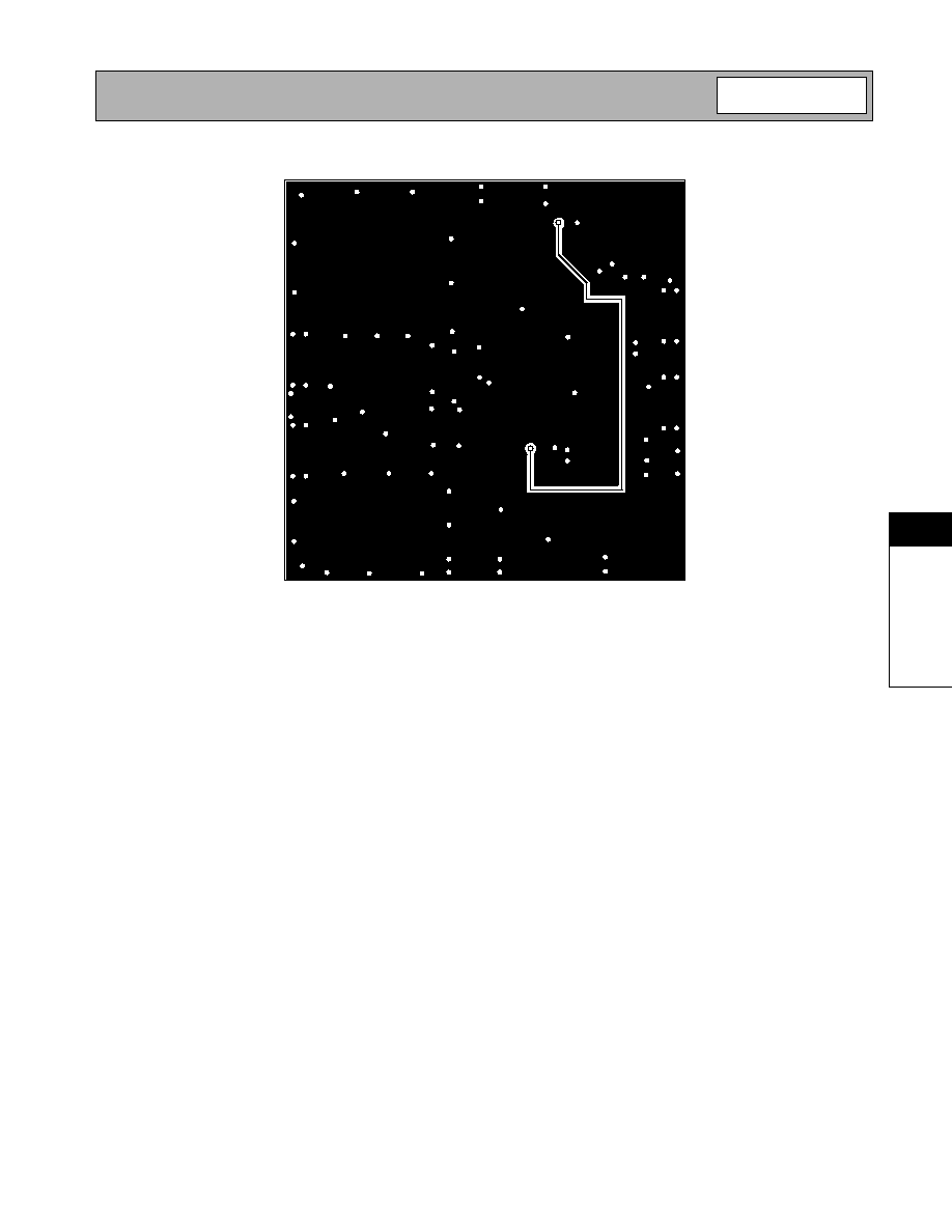
Evaluation Board Layout
3.025" x 3.025"
(Assembly, Top layer, Bottom layer)
7-9
RF2667
Rev A14 010622
7
Q
U
ADR
A
T
U
RE
DEM
O
DU
L
A
T
O
R
S
7-10
RF2667
Rev A14 010622
7
Q
U
ADR
A
T
U
RE
DEM
O
DU
L
A
T
O
R
S
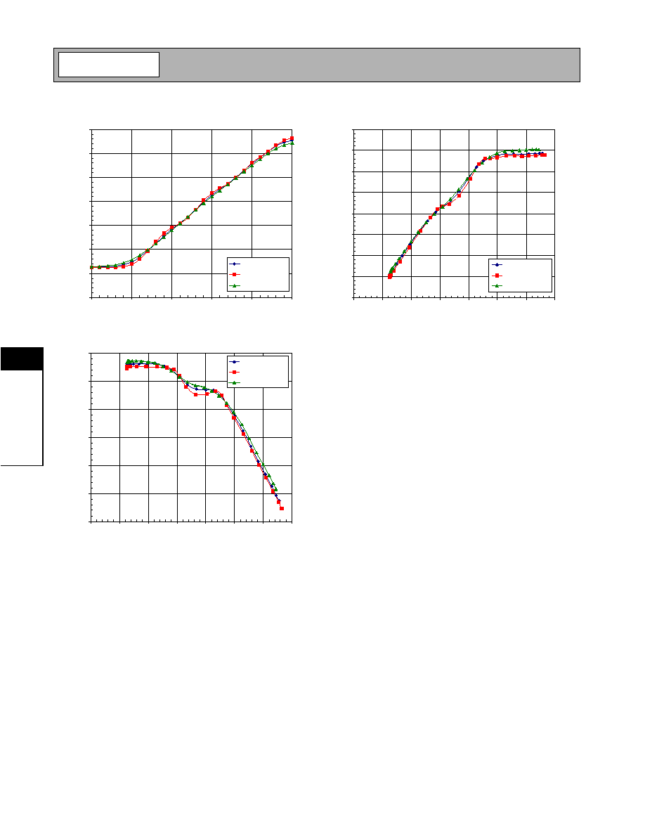
CDMA Cascade Conversion Gain versus Gain Control
Gain Control Voltage
(V
CC
=3.0V, 85MHz)
-80
-60
-40
-20
0
20
40
60
0
0.5
1
1.5
2
2.5
V
GC
(V)
Ga
i
n
(
d
B
)
Temp= 25 deg C
Temp= -30 deg C
Temp= 85 deg C
CDMA OIP3 versus Gain
(V
CC
=3.0V, 85 MHz)
-70
-60
-50
-40
-30
-20
-10
0
10
-80
-60
-40
-20
0
20
40
60
Gain (dB)
O
u
tput
IP
3
(
dB
m
)
Temp= 25 deg C
Temp= -30 deg C
Temp= 85 deg C
CDMA IIP3 versus Gain
(V
CC
=3.0V, 85 MHz)
-60
-50
-40
-30
-20
-10
0
-80
-60
-40
-20
0
20
40
60
Gain (dB)
Input
IP
3
(
dB
m
)
Temp= 25 deg C
Temp= -30 deg C
Temp= 85 deg C