 | –≠–ª–µ–∫—Ç—Ä–æ–Ω–Ω—ã–π –∫–æ–º–ø–æ–Ω–µ–Ω—Ç: RF2681 | –°–∫–∞—á–∞—Ç—å:  PDF PDF  ZIP ZIP |

¸
4-43
4
GEN
E
RA
L
P
URPO
S
E
A
M
P
L
IF
IE
RS
Preliminary
Product Description
Ordering Information
Typical Applications
Features
Functional Block Diagram
RF Micro Devices, Inc.
7628 Thorndike Road
Greensboro, NC 27409, USA
Tel (336) 664 1233
Fax (336) 664 0454
http://www.rfmd.com
Optimum Technology MatchingÆ Applied
Si BJT
GaAs MESFET
GaAs HBT
Si Bi-CMOS
SiGe HBT
Si CMOS
RF
O
U
T
NC
GC
VCC1
VCC2
VREG
RF
IN
NC
PD
GND
GND
GND
10
11
12
1
3
2
6
5
4
9
8
7
RF2681
W-CDMA LINEAR VARIABLE GAIN
DRIVER AMPLIFIER
∑ PA Driver Amplifier for W-CDMA Handsets
∑ General Purpose Driver Amplifier
The RF2681 is a linear variable gain amplifier specifically
designed for PA driver applications in W-CDMA handsets.
The device maintains excellent linearity over a 30dB gain
control range, while providing a maximum of 26 dB gain.
The IC is manufactured on an advanced Gallium Ars-
enide Heterojunction Bipolar Transistor Process and is
provided in an extremely small 3mmx3 mm, 12-pin, lead-
less chip carrier.
∑ 30dB Linear Gain Control Range
∑ 26dB Maximum Gain
∑ Single 2.7V to 3.3V Supply
∑ High Linearity Over Entire Gain Control
Range
∑ 9dBm Output Drive Available
RF2681
W-CDMA Linear Variable Gain Driver Amplifier
RF2681 PCBA
Fully Assembled Evaluation Board
4
Rev A1 010824
Dimensions in mm.
12∞
max
1.00
0.85
3.00
sq.
1.25
0.95
sq.
2
0.30
0.18
0.50
0.23
0.13
4 PLCS
0.80
0.65
NOTES:
Shaded Pin is Lead 1.
1
Dimension applies to plated terminal and is measured between 0.02 mm and
0.25 mm from terminal end.
2
5
Die thickness allowable: 0.305 mm max.
Package Warpage: 0.05 mm max.
4
Pin 1 identifier must exist on top surface of package by identification mark or
feature on the package body. Exact shape and size is optional.
3
0.65
0.30
4 PLCS
0.60
0.24 typ
0.75
0.50
0.05
0.01
Package Style: LCC, 12-Pin, 3x3

Preliminary
4-44
RF2681
Rev A1 010824
4
GEN
E
RA
L
P
URPO
S
E
A
M
P
L
IF
IE
RS
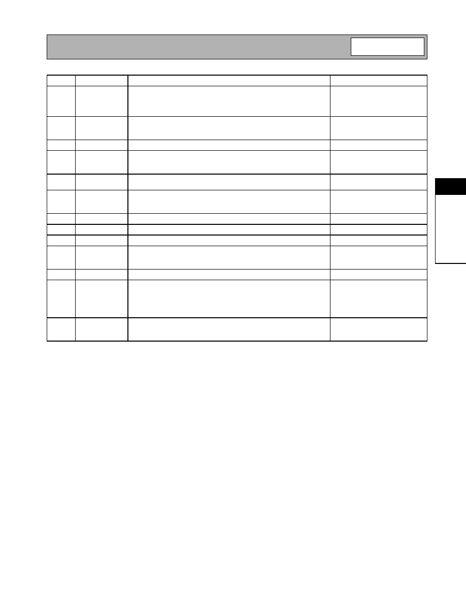
Absolute Maximum Ratings
Parameter
Rating
Unit
Supply Voltage
-0.5 to +3.6
V
DC
Operating Ambient Temperature
-40 to +85
∞C
Storage Temperature
-40 to +150
∞C
Parameter
Specification
Unit
Condition
Min.
Typ.
Max.
Overall
Usable Frequency Range
1800 to 2100
MHz
Linear Gain Control Range
30
dB
Gain Control Slope
40
dB/V
W-CDMA
Operating Frequency
1920 to 1980
MHz
Small Signal Gain
24
26
29
dB
V
GC
= 2.4V (Maximum Gain)
-7
-5
-3
V
GC
= 0V (Minimum Gain)
Output IP3
+22.0
+24.0
+26.0
dBm
V
GC
= 2.4V (Maximum Gain)
Noise Figure
3
dB
Small signal
Input VSWR
1.4:1
2:1
Over entire gain control range
Output VSWR
1.8:1
2:1
Maximum Linear Output Power
8
9
dBm
W-CDMA ACPR< -43dBc
ACPR1 (5MHz Offset)
-48
dBc
Over entire gain control range. P
IN
such that
P
OUT
=9dBm at maximum gain setting.
W-CDMA reverse link modulation.
ACPR2 (10MHz Offset)
-62
dBc
Power Supply
Supply Voltage
2.7
3.3
V
Operating range
Gain Control Voltage
0 to 2.4
V
Useful range
Supply Current
38
mA
V
CC
= 2.7V
V
GC
Current
220
µ
A
V
GC
= 2.4V (Maximum Gain)
1.7
mA
V
GC
= 0.2V
Caution! ESD sensitive device.
RF Micro Devices believes the furnished information is correct and accurate
at the time of this printing. However, RF Micro Devices reserves the right to
make changes to its products without notice. RF Micro Devices does not
assume responsibility for the use of the described product(s).
Preliminary
4-45
RF2681
Rev A1 010824
4
GEN
E
RA
L
P
URPO
S
E
A
M
P
L
IF
IE
RS
Pin
Function
Description
Interface Schematic
1
VCC1
DC supply for internal bias circuitry. This pin should be tied to VCC, and
must be bypassed with an RF capacitor. The trace length between the
pin and the bypass capacitor should be minimized. The ground side of
the capacitor should connect immediately to the ground plane.
2
VREG
DC supply for internal bias circuitry. This pin should be tied to a 2.7V
supply for proper operation. Increasing this voltage above 2.7V will
result in increased current drain and is not recommended.
3
VCC2
Same as pin 1.
4
PD
Power down pin. This pin should be brought below 1V for proper opera-
tion. The device is turned off when the voltage on this pin increases
above 2V.
5
NC
This pin is not internally connected, but should be grounded, if possi-
ble, to improve RF isolation. Please refer to the evaluation board layout.
6
RF IN
RF input pin. This pin requires external matching components, and is
DC-coupled. Please refer to the applications schematic for recom-
mended matching components.
7
GND
Ground
8
GND
Ground
9
GND
Ground
10
RF OUT
RF output pin. This pin requires an external matching network. VCC is
provided through an inductor of that network. Please refer to the appli-
cations schematic for recommended matching components.
11
NC
Same as pin 5.
12
GC
Gain control pin. This pin allows the gain of the amplifier to be varied in
a continuous "analog" fashion. With an applied voltage of 0.2V or less,
the amplifier exhibits the minimum gain. In the region between 0.2V
and 2.25V, the amplifier gain in dB depends on the voltage in a roughly
linear manner. Above 2.25V, the amplifier gain is set for maximum.
Pkg
Gnd
GND
Ground connection for the device "die flag". The backside of the pack-
age should be soldered to a top side ground pad which is connected to
the PC board ground plane through multiple vias.

Preliminary
4-46
RF2681
Rev A1 010824
4
GEN
E
RA
L
P
URPO
S
E
A
M
P
L
IF
IE
RS
Application Schematic
W-CDMA
10
11
12
1
3
2
6
5
4
9
8
7
47 nF
VREG
47 nF
1 nF
47 nF
VENABLE
3.6 nH
3 pF
2 nH
3 pF
10 nH
47 nF
VGC
47 nF
OUT
IN
V
CC
V
CC
V
CC
51
2.2 nH

Preliminary
4-47
RF2681
Rev A1 010824
4
GEN
E
RA
L
P
URPO
S
E
A
M
P
L
IF
IE
RS
Evaluation Board Schematic
(Download Bill of Materials from www.rfmd.com.)
10
11
12
1
3
2
6
5
4
9
8
7
VCC
C2
47 nF
VREG
C3
47 nF
C4
1 nF
VCC
C5
47 nF
VENABLE
L1
3.6 nH
C6
3 pF
50
µ
strip
J1
RF IN
L3
2 nH
C9
3 pF
L2
10 nH
C8
47 nF
VCC
VGC
C1
47 nF
J2
OUT
50
µ
strip
R1
51
L4
2.2 nH
P1
1
2
3
CON3
GND
P1-1
VCC
C10
1 uF
+
GND
P2
1
2
3
4
CON4
GND
P2-2
VCC ZLO
P2-1
VGC
P2-4
VCC
C11
1 uF
+
C12
1 uF
+
P3
1
2
3
CON3
GND
C13
1 uF
+
C14
1 uF
+
P3-1
VCC ZHI
P3-3
V ENABLE
Preliminary
4-48
RF2681
Rev A1 010824
4
GEN
E
RA
L
P
URPO
S
E
A
M
P
L
IF
IE
RS
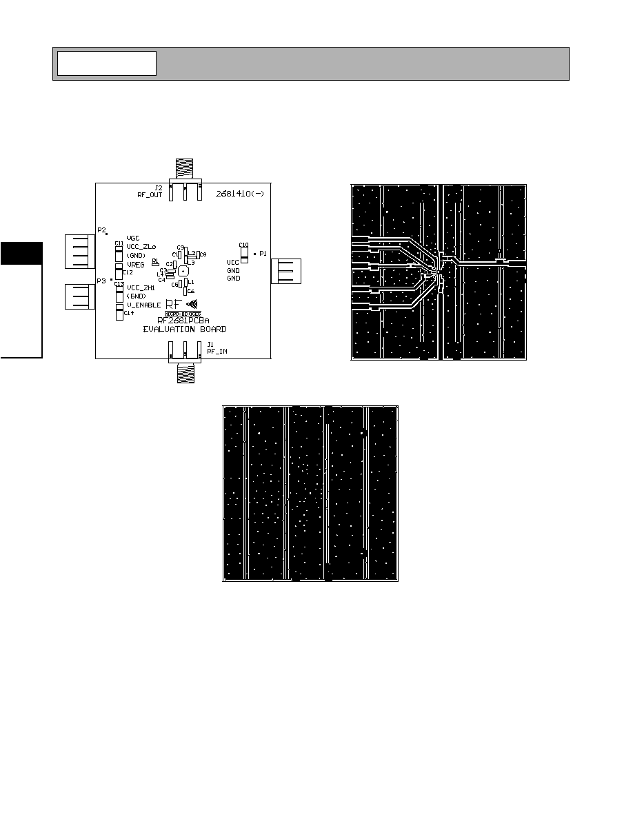
Evaluation Board Layout
Board Size 2.0" x 2.0"
Board Thickness 0.031", Board Material FR-4
Preliminary
4-49
RF2681
Rev A1 010824
4
GEN
E
RA
L
P
URPO
S
E
A
M
P
L
IF
IE
RS
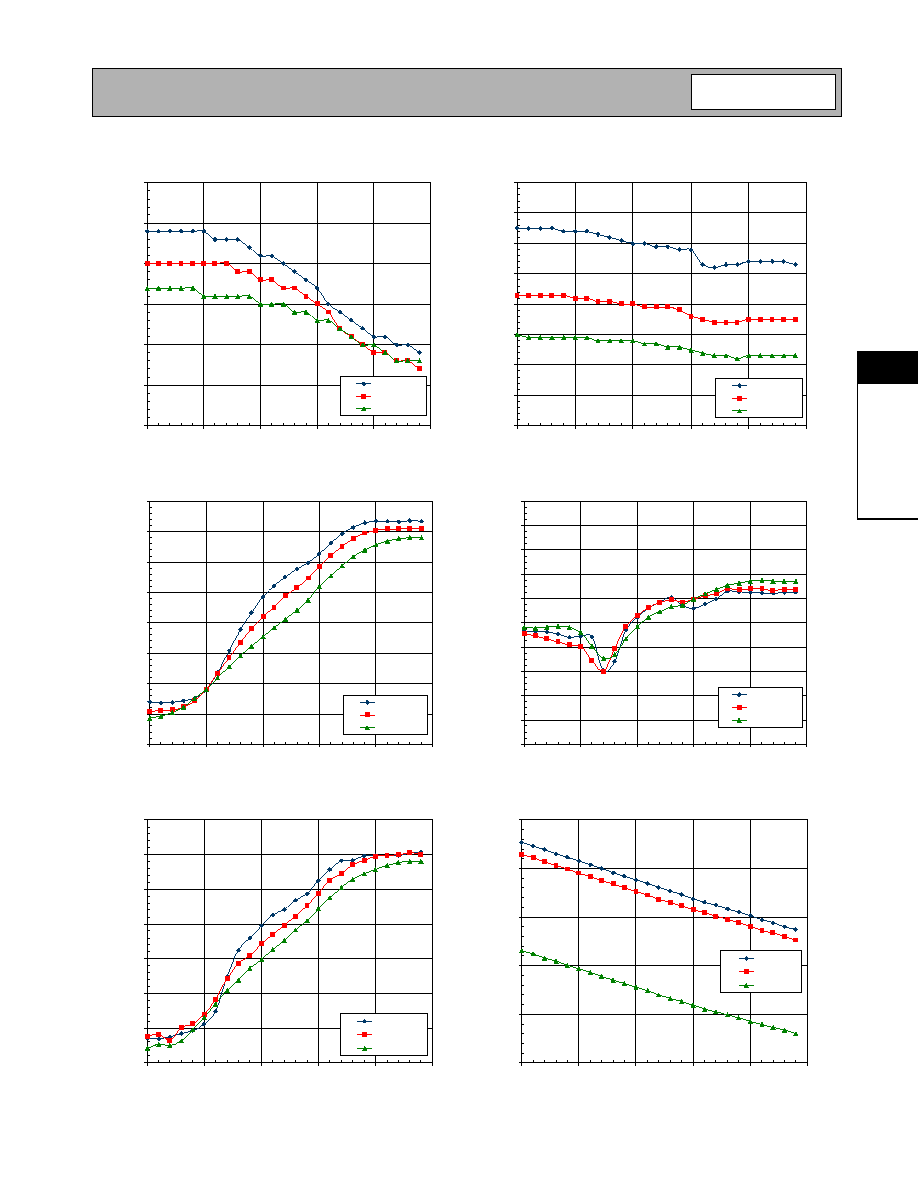
Input SWR versus V
GC
1.20
1.25
1.30
1.35
1.40
1.45
1.50
0.00
0.50
1.00
1.50
2.00
2.50
V
GC
(V)
SWR
SWR, -40∫
SWR, 25∫
SWR, 85∫
Output SWR versus V
GC
1.2
1.3
1.4
1.5
1.6
1.7
1.8
1.9
2.0
0.0
0.5
1.0
1.5
2.0
2.5
V
GC
(V)
SWR
SWR, -40∫
SWR, 25∫
SWR, 85∫
Gain versus V
GC
V
CC
= 2.7 V, Freq = 1950 MHz
-10.0
-5.0
0.0
5.0
10.0
15.0
20.0
25.0
30.0
0.0
0.5
1.0
1.5
2.0
2.5
V
GC
(V)
Gain
(dB)
Gain, -40∫
Gain, 25∫
Gain, 85∫
ACPR versus V
GC
Maximum Output Power: V
CC
= 2.7 V, Freq = 1950 MHz
-70.0
-66.0
-62.0
-58.0
-54.0
-50.0
-46.0
-42.0
-38.0
-34.0
-30.0
0.0
0.5
1.0
1.5
2.0
2.5
V
GC
(V)
ACPR
(dBc)
ACPR, -40∫
ACPR, 25∫
ACPR, 85∫
OIP3 versus V
GC
Maximum Output Power: V
CC
= 2.7 V, Freq = 1950 MHz
-5.0
0.0
5.0
10.0
15.0
20.0
25.0
30.0
0.0
0.5
1.0
1.5
2.0
2.5
V
GC
(V)
OIP3
(dBm)
OIP3, -40∫
OIP3, 25∫
OIP3, 85∫
I
CC
versus V
GC
V
CC
= 2.7 V, Freq = 1950 MHz
35.0
36.0
37.0
38.0
39.0
40.0
0.0
0.5
1.0
1.5
2.0
2.5
V
GC
(V)
I
CC
(mA)
Icc, -40∫
Icc, 25∫
Icc, 85∫

Preliminary
4-50
RF2681
Rev A1 010824
4
GEN
E
RA
L
P
URPO
S
E
A
M
P
L
IF
IE
RS