 | –≠–ª–µ–∫—Ç—Ä–æ–Ω–Ω—ã–π –∫–æ–º–ø–æ–Ω–µ–Ω—Ç: RF2861 | –°–∫–∞—á–∞—Ç—å:  PDF PDF  ZIP ZIP |

8-1
Product Description
Ordering Information
Typical Applications
Features
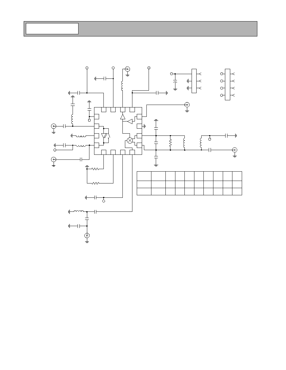
Functional Block Diagram
RF Micro Devices, Inc.
7628 Thorndike Road
Greensboro, NC 27409, USA
Tel (336) 664 1233
Fax (336) 664 0454
http://www.rfmd.com
Optimum Technology MatchingÆ Applied
Si BJT
GaAs MESFET
GaAs HBT
Si Bi-CMOS
SiGe HBT
Si CMOS
InGaP/HBT
GaN HEMT
SiGe Bi-CMOS
IF OUT+
IF OUT-
GND
LO IN
VCC
LO OUT
TX BUF
F
ENABLE
ENABLE
G2
LNA IN
LNA EMITTER
LNA OUT
ISET2
ISET1
G1
MI
X
I
N
8
7
6
5
3
4
1
2
13
14
15
16
10
9
12
11
RF2861
CDMA LOW NOISE AMPLIFIER/MIXER
900MHz DOWNCONVERTER
∑ CDMA/JCDMA Cellular Systems
∑ CDMA450 Handsets/Data Cards
∑ AMPS Cellular Systems
∑ General Purpose LNA and Downconverter
∑ Commercial and Consumer Systems
∑ Portable Battery-Powered Equipment
The RF2861 is a receiver front-end for CDMA cellular
applications, including JCDMA and CDMA450. It is
designed to amplify and downconvert RF signals, using a
three gain state LNA to obtain 17dB of stepped gain con-
trol. Features include digital control of LNA gain and
power down mode, along with an integrated TX LO buffer
amplifier. Another feature of the chip is adjustable IIP3 of
the LNA and mixer using off-chip current setting resistors
to allow for minimum DC current consumption. Noise fig-
ure, IIP3, and other specs are designed to be compatible
with the TIA/EIA 98D standard for CDMA cellular commu-
nications. The IC is manufactured on an advanced Silicon
Germanium Bi-CMOS process and is in a 3mmx3mm,
16-pin, QFN.
∑ 3mmx3mm LNA/Mixer Solution
∑ Adjustable LNA and Mixer Current/IIP3
∑ Meets IMD Tests with Three Gain
States/Two Logic Control Pins
∑ Integrated TX LO Buffer Amplifier
∑ Full ESD Protection on all Pins
RF2861
CDMA Low Noise Amplifier/Mixer 900MHz Down-
converter
RF2861 PCBA-410 Fully Assembled Evaluation Board
0
Rev A2 040107
0.90
0.85
0.05 C
0.05
0.00
0.70
0.65
12∞
MAX
-C-
SEATING
PLANE
1.50 TYP
0.10 C A
2 PLCS
-A-
3.00
0.10 C B
2 PLCS
1.37 TYP
0.10 C A
2 PLCS
2.75 SQ
0.10 C B
2 PLCS
3.00
-B-
0.60
0.24
TYP
0.50
0.30
PIN 1 ID
R.20
0.50
1.65
1.35
SQ.
0.10
C A B
M
0.30
0.18
2
NOTES:
1. Shaded lead is pin 1.
Dimension applies to plated terminal: to be measured
between 0.20 mm and 0.25 mm from terminal end.
2
Dimensions in mm.
Package Style: QFN, 16-Pin, 3x3

8-2
RF2861
Rev A2 040107
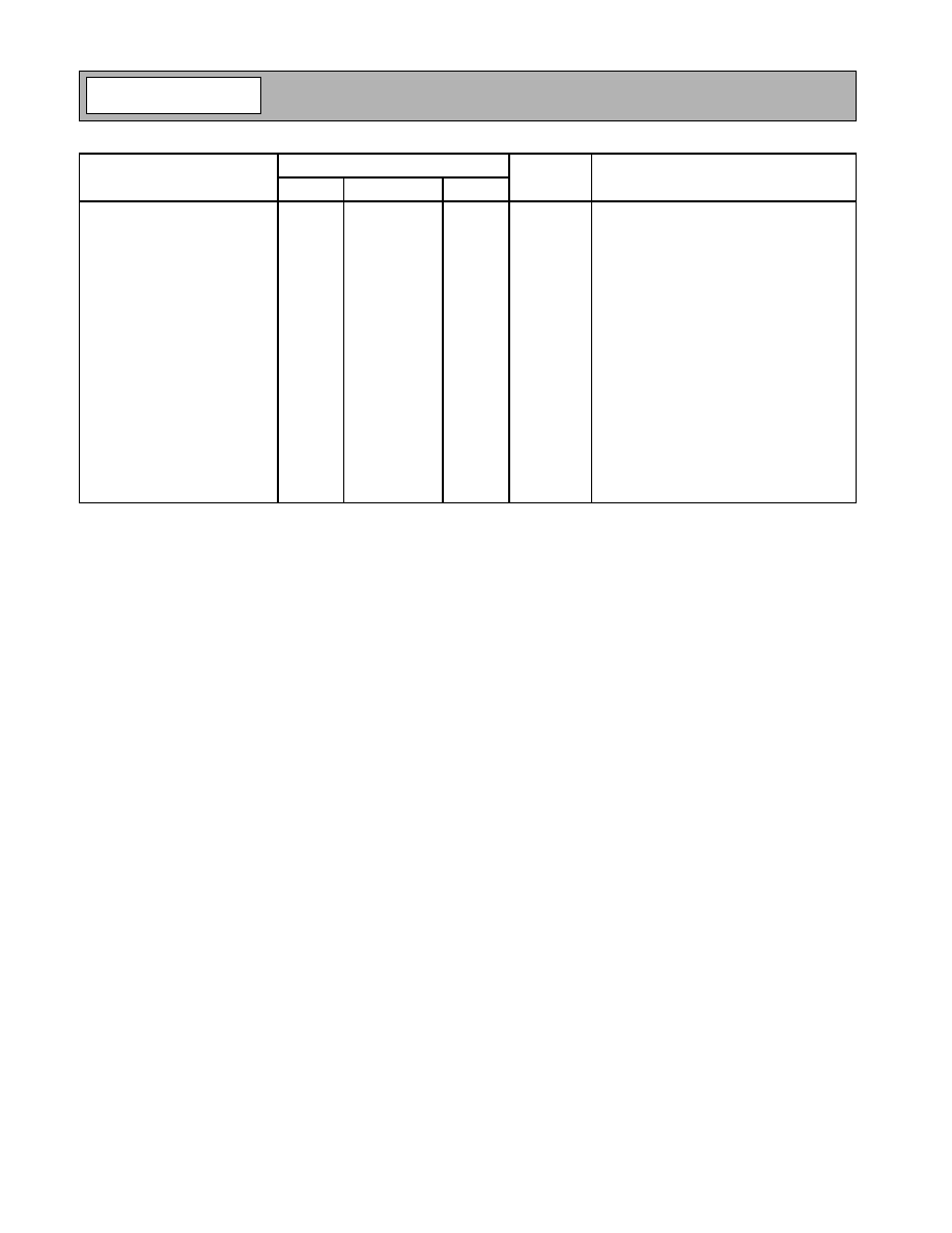
Absolute Maximum Ratings
Parameter
Rating
Unit
Supply Voltage
-0.5 to +5.0
V
DC
Input LO and RF Levels
+6
dBm
Operating Ambient Temperature
-40 to +85
∞C
Storage Temperature
-40 to +150
∞C
Parameter
Specification
Unit
Condition
Min.
Typ.
Max.
Overall
T = 25∞C, V
CC
=2.75V
RF Frequency Range
460 to 900
MHz
IF Frequency Range
0.1
400
MHz
Power Supply
Supply Voltage
2.65
2.75
3.15
V
Logic High
1.8
V
Logic Low
0.4
V
Cellular CDMA Band
JCDMA Band
Freq=869MHz to 894MHz
Freq=832MHz to 870MHz
LNA (High Gain)
LNA 50
match
Gain
13.0
14.5
16.0
dB
Noise Figure
1.1
1.3
dB
Input IP3
9.0
11.0
dBm
Current
7.0
mA
Isolation
18.5
dB
LNA (Mid Gain)
Gain
4.0
6.0
7.0
dB
Noise Figure
3.0
3.3
dB
Input IP3
7.0
9.0
dBm
Current
3.5
mA
Isolation
12.5
dB
LNA (Low Gain)
Gain
-4.0
-2.5
-1.0
dB
Noise Figure
2.5
4.0
dB
Input IP3
+25.0
+27.0
dBm
Current
0
mA
Isolation
1.0
dB
Mixer - CDMA/JCDMA/FM
IF tune set for nominal mixer gain, high IIP3
Gain
9.0
10.5
12.0
dB
Noise Figure
7.5
8.0
dB
184MHz IF (NF=8.3dB, 85MHz IF)
Input IP3
+6.0
+8.5
dBm
LO to RF Isolation
36
dB
LO=1064MHz
Mixer - CDMA/JCDMA/FM
IF tune set for high mixer gain, nominal IIP3
Gain
13.0
dB
Noise Figure
7.5
dB
184MHz IF (NF=8.3dB, 85MHz IF)
Input IP3
+6.5
dBm
LO to RF Isolation
36
dB
LO=1064MHz
Cascade - High Gain
Current
25
30
mA
TX LO Buffer Off
Caution! ESD sensitive device.
RF Micro Devices believes the furnished information is correct and accurate
at the time of this printing. However, RF Micro Devices reserves the right to
make changes to its products without notice. RF Micro Devices does not
assume responsibility for the use of the described product(s).

8-3
RF2861
Rev A2 040107
Parameter
Specification
Unit
Condition
Min.
Typ.
Max.
Cellular CDMA Band
JCDMA Band, cont'd
Other
LO-IF Isolation
30
dB
LO=1064MHz
RF-IF Isolation
45
dB
LNA Out to Mixer In Isolation
45
dB
LO-LNA In Isolation, Any State
40
dB
LO=1064MHz
Control Lines
Input Capacitance
1
pF
G1, G2, ENABLE, TX BUFF ENABLE
Local Oscillator Input
Cellular - CDMA or FM
Input Power
-10
-4
0
dBm
Input Frequency
685
710
MHz
IF=184MHz
1053
1078
MHz
IF=184MHz
784
809
MHz
IF=85MHz
954
979
MHz
IF=85MHz
Cellular - JCDMA
Input Power
-10
-4
0
dBm
Input Frequency
722
760
MHz
IF=110MHz
942
980
MHz
IF=110MHz
CDMA450
Input Power
-10
-4
0
dBm
Input Frequency
505
575
MHz
IF=85MHz
CDMA450 Band
Freq=463MHz to 467MHz
LNA (High Gain)
LNA 50
match
Gain
15.0
dB
Noise Figure
1.4
dB
Input IP3
+8.0
dBm
Current
8.7
mA
Isolation
18.5
dB
LNA (Mid Gain)
Gain
+2.5
dB
Noise Figure
2.9
dB
Input IP3
+14.0
dBm
Current
4.7
mA
Isolation
12.5
dB
LNA (Low Gain)
Gain
-4.0
dB
Noise Figure
4.0
dB
Input IP3
+25.0
dBm
Current
0
mA
Isolation
1.0
dB
Mixer
IF tune set for high mixer gain, nominal IIP3
Gain
12.0
dB
Noise Figure
7.5
dB
Input IP3
5.0
dBm
LO to RF Isolation
36
dB
LO=549MHz
CDMA450 Isolation
LO-IF Isolation
25
dB
LO=549MHz
RF-IF Isolation
40
dB
LNA Out to Mixer In Isolation
40
dB
LO-LNA In Isolation, Any State
30
dB
LO=549MHz
8-4
RF2861
Rev A2 040107
Parameter
Specification
Unit
Condition
Min.
Typ.
Max.
TX (Local Oscillator)
Buffer Output
Cellular - CDMA or FM
Output Power
-7
-5
-3
dBm
Single-ended 50
load
Output Frequency
685
710
MHz
IF=184MHz
1053
1078
MHz
IF=184MHz
784
809
MHz
IF=85MHz
954
979
MHz
IF=85MHz
Current Consumption
2
mA
Cellular - JCDMA
Output Power
-7
-5
-3
dBm
Single-ended 50
load
Output Frequency
722
760
MHz
IF=110MHz
942
980
MHz
IF=110MHz
Current Consumption
2
mA
CDMA450
Output Power
-7
-5
-3
dBm
Single-ended 50
load
Output Frequency
505
575
MHz
IF=85MHz
Current Consumption
2
mA
8-5
RF2861
Rev A2 040107
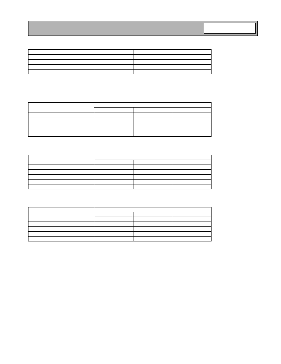
Gain Control Logic Table
Cell Band Cascaded Performance High Mixer Gain Nominal IIP3 (Typical Values for V
CC
=2.75V)
NOTE: All total current numbers include bias circuitry current of 1.5mA to 2.0mA (dependent on mode).
Cell Band Cascaded Performance Nominal Mixer Gain High IIP3 (Typical Values for V
CC
=2.75V)
CDMA450 Band Cascaded Performance (Typical Values for V
CC
=2.75V)
Gain State
ENABLE
G1
G2
High Gain
1
0
0
Mid Gain
1
1
0
Low Gain
1
1
1
Low Gain (alternate)
1
0
1
NOTES: All IDC current numbers include bias circuitry current of 1.5mA to 2.0mA (dependent on mode).
TX Buffer On: Add 2mA to total current.
Parameter
CELL CDMA
LNA (High Gain)
LNA (Mid Gain)
LNA (Low Gain)
Cascaded:
Gain (dB)
25.0
16.5
8.0
Noise Figure (dB)
2.1
6.3
12.5
Input IP3 (dBm)
-5.6
+2.0
+11.4
Total Current (mA)
25.0
21.5
18.0
NOTE: Assumes 2.5dB image filter insertion loss. The TX Buffer is off.
Parameter
CELL CDMA
LNA (High Gain)
LNA (Mid Gain)
LNA (Low Gain)
Cascaded:
Gain (dB)
22.5
14.0
5.5
Noise Figure (dB)
2.1
6.3
12.5
Input IP3 (dBm)
-3.7
+3.5
+13.3
Total Current (mA)
25.0
21.5
18.0
NOTE: Assumes 2.5dB image filter insertion loss. The TX Buffer is off.
Parameter
CDMA450
LNA (High Gain)
LNA (Mid Gain)
LNA (Low Gain)
Cascaded:
Gain (dB)
24.5
12.0
5.5
Noise Figure (dB)
2.2
8.5
14.0
Input IP3 (dBm)
-7.6
+4.5
+11.3
Total Current (mA)
29.5
25
21
NOTE: Assumes 2.5dB image filter insertion loss. The TX Buffer is off.
8-6
RF2861
Rev A2 040107
Pin
Function
Type Description
Interface Schematic
1
G2
DI
Gain control logic input. See logic control table.
2
LNA IN
AI
Cellular LNA input.
3
LNA
EMITTER
AO
Cellular LNA emitter. A small inductor connects this pin to
ground. Cellular LNA gain can be adjusted by the inductance.
See pin 2.
4
LNA OUT
AO
Cellular LNA output. Simple external L-C components
required for matching and VCC supply.
See pin 2.
5
ISET2
AO
An external resistor connected to this pin sets the current of
the mixer. Increasing resistance decreases current.
6
ISET1
AO
An external resistor connected to this pin sets the current of
the LNA. Increasing resistance decreases current.
7
G1
DI
Gain control logic input. See logic control table.
8
MIX IN
AI
Cellular mixer RF single-end input.
9
IF OUT+
AO
CDMA IF output. Open collector.
10
IF OUT-
AO
CDMA IF output. Open collector.
See pin 9.
11
GND
P
Ground.
12
LO IN
AI
LO single-end input. Matched to 50
.
13
VCC
P
LO amplifier VCC external bypass capacitor may be required.
14
LO OUT
AO
LO output. Internal DC block. Drives 50
.
15
TX BUFF
ENABLE
DI
Logic input. High enables TX LO output buffer amplifiers.
16
ENABLE
DI
Logic input. Low level powers down the IC.
Pkg
Base
GND
P
Ground connection. The backside of the package should be
soldered to a top side ground pad which is connected to the
ground plane with multiple vias.
Legend:
DI=Digital Input from Baseband Chip
AI=Analog Input
P=V
CC
or GND
AO=Analog Output
G2
LNA IN
V
CC
LNA OUT
LNA EMITTER
G1
MIX IN
IF OUT+
IF OUT-
LO IN
70
TX BUFF ENABLE
ENABLE
8-7
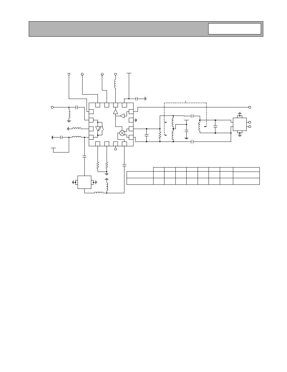
RF2861
Rev A2 040107
Application Schematic
Differential IF Matching
C1
R1
L2
L1
C2
C3
L3
IF Saw
4
5
9
10
IF+
IF-
LO IN
2.2 nH
LO
OUT
TX BUFF
ENABLE
ENABLE
G2
CELL LNA IN
1.2 nH
10 nH
3.9 pF
RF Saw
4
5
6
3
GND
GND
GND
GND
IN
OUT
2
1
9.1 k
20 k
22 nH
33 nF
DNI
33 nF
33 nF
33 nF
8
7
6
5
3
4
1
2
13
14
15
16
10
9
12
11
V
CC
V
CC
V
CC
G1
33 nH
33 nF
0603 Wire-wound Inductors
DNI
C1
R1
L1
L2
C2
C3
L3
85 MHz IF (LO
FREQ=965 MHz)
184 MHz IF (LO
FREQ=1064 MHz)
22 pF 2.7 k
72 nH 72 nH 5.1 pF 5.1 pF 220 nH
5.0 pF 2.7 k
55 nH 55 nH
10 pF
10 pF
43 nH
IF SAW FILTER
SAWTEK 855845
EPCOS B4955

8-8
RF2861
Rev A2 040107
Application Schematic
Single-End Matching
8
7
6
5
3
4
1
2
13
14
15
16
10
9
12
11
C2
R1
L1
33 nF
L2
LO IN
2.2 nH
LO
OUT
33 nF
10 nH
3.9 pF
RF Saw
4
5
6
3
GND
GND
GND
GND
IN
OU
T
2
1
9.1 k
20 k
22 nH
33 nF
C1
C3
V
CC
C4
IF Saw
4
5
9
10
IF+
IF-
V
CC
V
CC
G1
TX BUFF
ENABLE
ENABLE
G2
CELL LNA IN
1.2 nH
33 nF
33 nH
DNI
C5
L3
33 nF
+
85 MHz IF (LO
FREQ=965 MHz)
43
43
DNI
2.7
72
72
5.1
DNI
220
SAWTEK 855845
184 MHz IF (LO
FREQ=1064 MHz)
13
13
DNI
2.7
55
55
10
DNI
43
EPCOS B4955
C1
(pF)
C2
(pF)
C3
R1
(k
)
L1
(nH)
L2
(nH)
C4
(pF)
C5
L3
(nH)
IF SAW FILTER

8-9
RF2861
Rev A2 040107
Application Schematic
Single-End Matching
CDMA450 Band
8
7
6
5
3
4
1
2
13
14
15
16
10
9
12
11
C2*
R1*
L2*
33 nF
L1*
LO IN
2.2 nH
LO
OUT
33 nF
27 nH
27 pF
RF Saw
4
5
6
3
GND
GND
GND
GND
IN
OUT
2
1
6.8 k
22 k
100 pF
C1*
C3*
V
CC
C4*
IF Saw
4
5
9
10
IF+
IF-
V
CC
V
CC
G1
TX BUFF
ENABLE
ENABLE
G2
CELL LNA IN
5.6 nH
33 nF
33 nH
33 nF
+
33 nH
2.2 pF
+
C5*
L3*
*Values determined by choice of IF SAW.
0603 Wire-wound Inductors
8-10
RF2861
Rev A2 040107
Evaluation Board Schematic
C35
R2
L11
C17
L17
2.2 nH
TX BUFF
ENABLE
ENABLE
L24
1.2 nH
L21
10 nH
C9
22.0 nH
R6
9.1 k
R4
20.0 k
L3
DNI
C2
33 nF
C25
33 nF
C6
33 nF
C7
33 nF
8
7
6
5
3
4
1
2
13
14
15
16
10
9
12
11
G1
L1
33 nH
C4
33 nF
C1
33 nF
C8
1 pF
J3
CELL MIX IN
VCC
3.9 pF
J2
CELL LNA OUT
J1
CELL LNA IN
C55
33 nF
G2
C54
33 nF
C46
33 nF
J6
LO OUT
VCC
J5
LO IN
C3
C5
L6
VCC
C22
J4
CDMA IF
DNI
DNI
C35
(pF)
85
184
Freq IF
(MHz)
965
1064
Freq LO
(MHz)
47
13
C3
(pF)
47
13
C5
(pF)
150
82
L11
(nH)
180
150
L6
(nH)
33
33
C22
(nF)
8
11
C17
(pF)
5.1
2.7
R2
(k
)
P1
1
2
3
CON3
P1-1
VCC1
GND
GND
C20
1 uF
+
P2
1
2
3
4
CON4
P2-4
G2
P2-3
G1
P2-2
TX BUF EN
P2-1
ENABLE
8-11
RF2861
Rev A2 040107
Evaluation Board Schematic
CDMA450 Band
C35
R2
L11
C17
L17
2.2 nH
TX BUFF
ENABLE
ENABLE
L24
5.6 nH
C9
2.2 pF
R6
6.8 k
R4
22 k
L3
33 nH
C2
33 nF
C25
33 nF
C6
33 nF
C7
33 nF
8
7
6
5
3
4
1
2
13
14
15
16
10
9
12
11
G1
L1
33 nH
C4
33 nF
C1
33 nF
C8
DNI
J3
CELL MIX IN
VCC
2.7 pF
J2
CELL LNA OUT
J1
CELL LNA IN
C55
33 nF
G2
C54
33 nF
C46
33 nF
J6
LO OUT
VCC
J5
LO IN
C3
C5
L6
VCC
C22
J4
CDMA IF
85
Freq IF
(MHz)
549
Freq LO
(MHz)
91
C3
(pF)
91
C5
(pF)
68
L11
(nH)
270
L6
(nH)
33
C22
(nF)
27
C17
(pF)
DNI
C35
(pF)
6.8
R2
(k
)
P1
1
2
3
CON3
P1-1
VCC1
GND
GND
C20
1 uF
+
P2
1
2
3
4
CON4
P2-4
G2
P2-3
G1
P2-2
TX BUF EN
P2-1
ENABLE
L21
27 nH

8-12
RF2861
Rev A2 040107
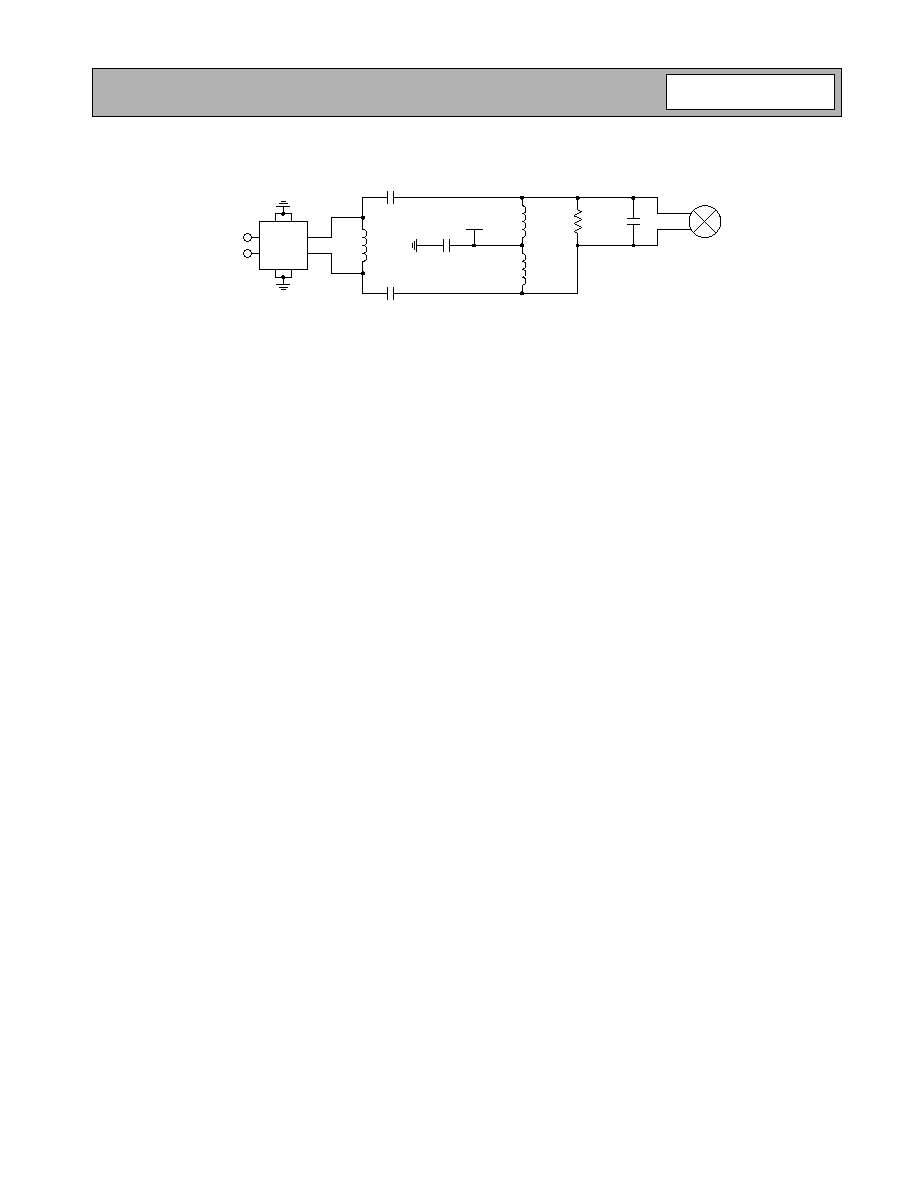
IF Output Interface Network
Single-End IF Matching
L1, C1, C2, and R form a current combiner which performs a differential to single-ended conversion at the IF frequency
and sets the output impedance. In most cases, the resonance frequency is independent of R and can be set according to
the following equation:
Where C
EQ
is the equivalent stray capacitance and capacitance looking into pins 9 and 10. An average value to use for
C
EQ
is 2.5pF.
R can then be used to set the output impedance according to the following equation:
where R
OUT
is the desired output impedance and R
P
is the parasitic equivalent parallel resistance of L1.
C
2
should first be set to 0 and C1 should be chosen as high as possible (not greater than 39pF), while maintaining an R
P
of L1 that allows for the desired R
OUT
. If the self-resonant frequencies of the selected C1 produce unsatisfactory linearity
performance, their values may be reduced and compensated for by including C2 capacitor with a value chosen to main-
tain the desired F
IF
frequency.
L2 and C3 serve dual purposes. L2 serves as an output bias choke, and C3 serves as a series DC block.
In addition, L2 and C3 may be chosen to form an impedance matching network if the input impedance of the IF filter is
not equal to R
OUT
. Otherwise, L2 is chosen to be large (suggested 120nH) and C3 is chosen to be large (suggested
22nF) if a DC path to ground is present in the IF filter, or omitted if the filter is DC-blocked.
IF-
IF+
C2
R
L1
L2
V
CC
33 nF
C3
IF Saw
4
5
9
10
IF+
IF-
C1
C1
f
IF
1
L1
2
------ C
1
2C
2
C
EQ
+
+
(
)
2
-----------------------------------------------------------
=
R
1
4 R
OUT
---------------------
1
R
P
------
≠
1
≠
=
8-13
RF2861
Rev A2 040107
Differential IF Matching
L1 and C1 are chosen to resonate at the desired IF frequency. C1 can be omitted and the value of L1 increased and uti-
lized solely as a choke to provide V
CC
to the open-collector outputs, but it is strongly recommended that at least some
small-valued C1 (a few pF) be retained for better mixer linearity performance. R is normally selected to match the input
impedance of the IF filter. However, mixer performance can be modified by selecting an R value that is different from the
IF filter input impedance, and inserting a conjugate matching network between the Resistive Output Network and the IF
filter.
C2 serve dual purposes. C2 serves as a series DC block when a DC path to ground is present in the IF filter. In addition,
C2 may be chosen to improve the combine performance of the mixer and IF filter. L2 should choose to resonate with the
internal capacitance of the SAW filter. Usually, SAW filter has some capacitance. Otherwise, L2 could be eliminated.
A practical approach to obtain the differential matching is to tune the mixer to the correct load point for gain, IIP3, and NF
using the single-end current combiner method. Second, use the component values found in the single-end approach as
starting point for the differential matching. The two-shunt capacitors in the single-end could be converted in a parallel
capacitor and the parallel inductor in the single-end need to be converted in two-choke inductor. Third, set the DC block
capacitors (C2) in the differential-end matching to a high value (i.e., 100pF) and retune the resonate circuit (C1 & L1)
and the resistor (R) for optimal performance. After optimal performance is achieved and if performance is not satisfac-
tory, decrease the series capacitors until optimal performance is achieved.
C1
R
L1
L1
V
CC
33 nF
C2
C2
IF+
IF-
L2
IF Saw
4
5
9
10
IF-
IF+
8-14
RF2861
Rev A2 040107
PCB Design Requirements
PCB Surface Finish
The PCB surface finish used for RFMD's qualification process is electroless nickel, immersion gold. Typical thickness is
3
µ
inch to 8
µ
inch gold over 180
µ
inch nickel.
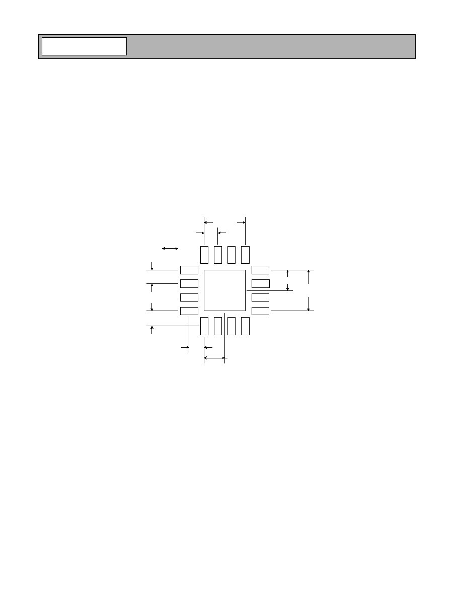
PCB Land Pattern Recommendation
PCB land patterns are based on IPC-SM-782 standards when possible. The pad pattern shown has been developed and
tested for optimized assembly at RFMD; however, it may require some modifications to address company specific
assembly processes. The PCB land pattern has been developed to accommodate lead and package tolerances.
PCB Metal Land Pattern
A = 0.64 x 0.28 (mm) Typ.
B = 0.28 x 0.64 (mm) Typ.
C = 1.50 (mm) Sq.
B
B
B
B
A
A
A
A
B
B
B
B
A
A
A
A
C
Pin 16
Pin 1
Pin 12
Pin 8
Dimensions in mm.
0.50 Typ.
1.50 Typ.
0.50 Typ.
0.55 Typ.
0.55 Typ.
0.75 Typ.
0.75 Typ.
1.50
Typ.
Figure 1. PCB Metal Land Pattern (Top View)