
8-1
Product Description
Ordering Information
Typical Applications
Features
Functional Block Diagram
RF Micro Devices, Inc.
7628 Thorndike Road
Greensboro, NC 27409, USA
Tel (336) 664 1233
Fax (336) 664 0454
http://www.rfmd.com
Optimum Technology MatchingÆ Applied
Si BJT
GaAs MESFET
GaAs HBT
Si Bi-CMOS
SiGe HBT
Si CMOS
InGaP/HBT
GaN HEMT
SiGe Bi-CMOS
16
15
14
13
11
12
9
10
5
6
7
8
2
1
4
3
IF OUT+
IF OUT-
GND
LO IN
VCC
LO O
U
T
TX BUFF
EN
ABLE
EN
ABLE
LNA GAIN
LNA IN
LNA EMITTER
LNA OUT
MIX GAIN
ISET2
ISET1
MIX IN
RF2870
CDMA LOW NOISE AMPLIFIER/MIXER
900MHz DOWNCONVERTER
∑ CDMA Cellular Systems
∑ JCDMA Cellular Systems
∑ AMPS Cellular Systems
∑ General Purpose Downconverter
∑ Commercial and Consumer Systems
∑ Portable Battery-Powered Equipment
The RF2870 is a receiver front-end for CDMA cellular
applications. It is designed to amplify and downconvert
RF signals, while providing 28.5dB of stepped gain con-
trol range. Features include digital control of LNA gain,
mixer gain, and power down mode. Another feature of the
chip is adjustable IIP3 of the mixer using an off-chip cur-
rent setting resistor. Noise figure, IP3, and other specs
are designed to be compatible with the IS-98B interim
standard for CDMA cellular communications. The IC is
manufactured on an advanced Silicon Germanium Bi-
CMOS process and is assembled in a 3mmx3mm, 16-
pin, QFN package.
∑ 3mmx3mm LNA/Mixer Solution
∑ Adjustable Mixer Current/IIP3
∑ Meets IMD Tests with Three Gain
States/Two Logic Control Lines
∑ Integrated TX LO Buffer Amplifier
∑ All Pins ESD Protected
RF2870
CDMA Low Noise Amplifier/Mixer 900MHz Downcon-
verter
RF2870 PCBA Fully Assembled Evaluation Board
0
Rev A8 030507
0.90
0.85
0.05 C
0.05
0.00
0.70
0.65
12∞
MAX
-C-
SEATING
PLANE
1.50 TYP
0.10 C A
2 PLCS
-A-
3.00
0.10 C B
2 PLCS
1.37 TYP
0.10 C A
2 PLCS
2.75 SQ
0.10 C B
2 PLCS
3.00
-B-
0.60
0.24
TYP
0.50
0.30
PIN 1 ID
R.20
0.50
1.65
1.35
SQ.
0.10
C A B
M
0.30
0.18
2
NOTES:
1. Shaded lead is pin 1.
Dimension applies to plated terminal: to be measured
between 0.20 mm and 0.25 mm from terminal end.
2
Dimensions in mm.
Package Style: QFN, 16-Pin, 3x3
8-2
RF2870
Rev A8 030507
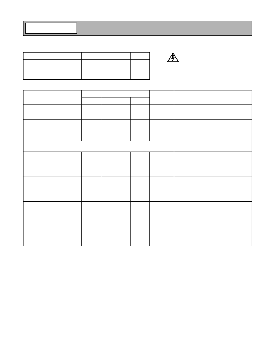
Absolute Maximum Ratings
Parameter
Rating
Unit
Supply Voltage
-0.5 to +5.0
V
DC
Input LO and RF Levels
+6
dBm
Operating Ambient Temperature
-40 to +85
∞C
Storage Temperature
-40 to +150
∞C
Parameter
Specification
Unit
Condition
Min.
Typ.
Max.
Overall
T = 25∞C, V
CC
=2.75V
RF Frequency Range
800 to 900
MHz
IF Frequency Range
0.1
400
MHz
Power Supply
Supply Voltage, V
S
2.65
2.75
3.15
V
Logic High
1.8
V
S
+0.6
V
Logic Low
0.4
V
Cellular Band
JCDMA Band
Freq=869MHz to 894MHz
Freq=832MHz to 870MHz
LNA (On)
LNA 50
match
Gain
13.0
14.5
16.0
dB
Noise Figure
1.1
1.3
dB
Input IP3
+9.0
+11.5
dBm
Isolation
23
dB
LNA (Off)
Gain
-4.0
-3.0
-2.0
dB
Noise Figure
3.0
4.0
dB
Input IP3
+20.0
+25.0
dBm
Isolation
3.5
dB
Mixer - CDMA/JCDMA/FM
Gain
11.5
13.0
14.5
dB
Mixer Preamp ON
0.5
2.0
3.5
dB
Mixer Preamp OFF
Noise Figure
6.5
7.5
dB
Mixer Preamp ON (TX Buffer OFF)
14.0
16.0
dB
Mixer Preamp OFF
Input IP3
+1.0
+3.0
dBm
Mixer Preamp ON
+12.5
+14.5
dBm
Mixer Preamp OFF
LO to RF Isolation
36
dB
Mixer Preamp ON
dB
Mixer Preamp OFF
Caution! ESD sensitive device.
RF Micro Devices believes the furnished information is correct and accurate
at the time of this printing. However, RF Micro Devices reserves the right to
make changes to its products without notice. RF Micro Devices does not
assume responsibility for the use of the described product(s).

8-3
RF2870
Rev A8 030507
Parameter
Specification
Unit
Condition
Min.
Typ.
Max.
Cellular Band
JCDMA Band, cont'd
Other
LO-IF Isolation
30
dB
RF-IF Isolation
40
dB
LNA Out to Mixer In Isolation
40
dB
LO-LNA In Isolation, Any State
35
dB
Control Lines
Input Capacitance
1
pF
LNA GAIN, ENABLE, MIX GAIN, TX BUFF
ENABLE
Local Oscillator Input
Cellular - CDMA or FM
Input Power
-10
-4
0
dBm
Input Frequency
685
710
MHz
IF=184MHz
1053
1078
MHz
IF=184MHz
784
809
MHz
IF=85MHz
954
979
MHz
IF=85MHz
Cellular - JCDMA
Input Power
-10
-4
0
dBm
Input Frequency
722
760
MHz
IF=110MHz
942
980
MHz
IF=110MHz
TX (Local Oscillator)
Buffer
Cellular - CDMA or FM
Output Power
-9.0
-5.5
-2.0
dBm
Single-ended 50
load
Output Frequency
685
710
MHz
IF=184MHz
1053
1078
MHz
IF=184MHz
784
809
MHz
IF=85MHz
954
979
MHz
IF=85MHz
Current Consumption
2
mA
Cellular - JCDMA
Output Power
-9
-5.5
dBm
Single-ended 50
load
Output Frequency
722
760
MHz
IF=110MHz
942
980
MHz
IF=110MHz
Current Consumption
2
mA

8-4
RF2870
Rev A8 030507
Evaluation Board Current Measurement (Typical Values for V
CC
=2.75V)
NOTES:
All IDC current numbers include bias circuitry current of 1.5mA to 2.0mA (dependent on mode).
TX Buffer On: Add 2.4mA to total current.
Cascaded Performance (Typical Values for V
CC
=2.75V)
NOTE: All total current numbers include bias circuitry current of 1.5mA to 2.0mA (dependent on mode).
Gain Control State Table
ENABLE
LNA
GAIN
MIX
GAIN
TX BUFF
ENABLE
IDC
(mA)
Gain Control State
Power Down
0
X
X
X
<0.01
LNA On, Mixer Preamp On,
TX Buffer Off
1
0
0
0
26.5
LNA On, Mixer Preamp Off,
TX Buffer Off
1
0
1
0
20.6
LNA Bypassed, Mixer Preamp On,
TX Buffer Off
1
1
1
0
20.9
LNA Bypassed, Mixer Preamp Off,
TX Buffer Off
1
1
0
0
15.0
CELL CDMA
Parameter
LNA ON
LNA OFF
LNA ON
LNA OFF
Mixer Preamp On
Mixer Preamp Off
Cascaded:
Gain (dB)
25.0
7.5
14.0
-3.5
Noise Figure (dB)
1.9
12.0
4.5
19.5
Input IP3 (dBm)
-9.0
+8.4
+2.0
+18.8
LO to IF Isolation (dB)
30
30
30
30
IF1 to RF Isolation (dB)
40
40
40
40
IF2 to RF Isolation (dB)
40
40
40
40
LO to LNA IN Isolation (dB)
45
45
45
45
Total Current (mA)
26.5
20.9
20.6
15.0
NOTE: Assumes 2.5dB image filter insertion loss. The TX Buffer Enable is off.
Corresponding Device State
Gain State
LNA Gain
Logic Input
Mix Gain
Logic Input
LNA
Amplifier
Mixer
Preamp
Comments
High Gain
0
0
On
On
IMD Test 1 and 2
Mid Gain
0
1
On
Off
IMD Test 3 and 4
Low Gain
1
1
Off
On
IMD Test 5 and 6
Ultra-Low Gain
1
0
Off
Off

8-5
RF2870
Rev A8 030507
Pin
Function
Description
Interface Schematic
1
IF OUT+
CDMA IF output. Open collector.
2
IF OUT-
CDMA IF output. Open collector.
See pin 1.
3
GND
4
LO IN
LO single-end input. Matched to 50
.
5
VCC
External bypass capacitor may be required.
6
LO OUT
LO output. Internal DC block. Drives 50
.
7
TX BUFF
ENABLE
Logic input. High enables TX LO output buffer amplifiers.
8
ENABLE
Logic input. Low level powers down the IC.
9
LNA GAIN
Logic input. See Gain Control State table.
10
LNA IN
Cellular LNA input.
11
LNA
EMITTER
Cellular LNA emitter. A small inductor connects this pin to ground. Cel-
lular LNA gain can be adjusted by the inductance.
See pin 10.
12
LNA OUT
Cellular LNA output. Simple external L-C components required for
matching and VCC supply.
See pin 10.
13
MIX GAIN
Logic input. See Gain Control State table.
14
ISET2
An external resistor R2 connected to this pin sets the current of the
mixer. Decreasing resistance increases current.
15
ISET1
Sets internal voltage reference. External resistor required.
16
MIX IN
Cellular mixer RF single-end input. Matched to 50
.
Pkg
Base
GND
Ground connection. The backside of the package should be soldered to
a top side ground pad which is connected to the ground plane with mul-
tiple vias.
CDMA+
CDMA-
LO IN
70
TX BUF
ENABLE
LNA GAIN
CELL LNA IN
V
CC
CELL LNA OUT
CELL LNA EMITTER
MIX GAIN
CELL MIX IN