
NO
T
FOR
N
EW
DE
SI
GNS
11-139
Product Description
Ordering Information
Typical Applications
Features
Functional Block Diagram
RF Micro Devices, Inc.
7628 Thorndike Road
Greensboro, NC 27409, USA
Tel (336) 664 1233
Fax (336) 664 0454
http://www.rfmd.com
Optimum Technology MatchingÆ Applied
Si BJT
GaAs MESFET
GaAs HBT
Si Bi-CMOS
SiGe HBT
Si CMOS
InGaP/HBT
GaN HEMT
SiGe Bi-CMOS
13 16
8
6
Linear
RSSI
4
2
25 26
Prescaler
˜
64
Phase
Detector &
Charge Pump
29
10
9
17
18
12
11
23 24
IF
2 I
N
IF1 OU
T
IF2 B
P
+
IF2 B
P
-
IF1 B
P
-
IF1 B
P
+
IF1 IN
+
IF1 IN
-
IF2 OU
T
DE
MO
D I
N
MIX OUT
MIX IN
LNA OUT
RX IN
RES
N
T
R
+
LOO
P
FLT
RES
N
T
R
-
32
PD
DC
BIAS
30 OSC B
31 OSC E
21 RSSI
20 MUTE
22 FM OUT
RF2917
433/868/915MHz
FM/FSK RECEIVER
∑ Wireless Meter Reading
∑ Keyless Entry Systems
∑ 433/868/915MHz ISM Band Systems
∑ Remote Data Transfers
∑ Wireless Security Systems
The RF2917 is a monolithic integrated circuit intended for
use as a low cost FM or FSK receiver. The device is pro-
vided in 32-lead plastic packaging and is designed to pro-
vide a fully functional FM receiver. The chip is intended
for analog or digital applications in the North American
915MHz ISM band and European 433MHz and 868 MHz
ISM bands. The integrated VCO,
˜
64 prescaler, and ref-
erence oscillator require only the addition of an external
crystal to provide a complete phase-locked oscillator for
single channel applications. The selection of linear FM
output or digital FSK output is done with the mute pin.
∑ Fully Monolithic Integrated Receiver
∑ 2.7V to 5.0V Supply Voltage
∑ Narrowband and Wideband FSK
∑ 300MHz to 1000MHz Frequency Range
∑ Power Down Capability
∑ Analog or Digital Output
RF2917
433/868/915MHz FM/FSK Receiver
RF2917 PCBA-L Fully Assembled Evaluation Board, 433MHz
RF2917 PCBA-M Fully Assembled Evaluation Board, 868MHz
RF2917 PCBA-H Fully Assembled Evaluation Board, 915MHz
0
Rev B4 021008
7∞ MAX
0∞ MIN
+ 0.15
0.10
0.60
0.127
7.00
+ 0.20 sq.
5.00
+ 0.10 sq.
0.22
+ 0.05
Dimensions in mm.
0.15
0.05
-A-
1.40
+ 0.05
0.50
Package Style: LQFP, 32-Pin, 5x5
NOT FOR NEW DESIGNS
!

11-140
RF2917
Rev B4 021008
NO
T
FOR
N
EW
DE
SI
GNS
Absolute Maximum Ratings
Parameter
Ratings
Unit
Supply Voltage
-0.5 to +5.5
V
DC
Control Voltages
-0.5 to +5.0
V
DC
Input RF Level
+10
dBm
Output Load VSWR
50:1
Operating Ambient Temperature
-40 to +85
∞C
Storage Temperature
-40 to +150
∞C
Parameter
Specification
Unit
Condition
Min.
Typ.
Max.
Overall
T=25 ∞C, V
CC
=3.6V, Freq=915MHz
RF Frequency Range
300 to 1000
MHz
VCO and PLL Section
VCO Frequency Range
300 to 1000
MHz
PLL Lock Time
10
ms
The PLL lock time is set externally by the
bandwidth of the loop filter and start up of
the crystal.
PLL Phase Noise
-74
-98
dBc/Hz
dBc/Hz
915MHz, 5kHz loop BW, 10kHz offset
915MHz, 5kHz loop BW, 100kHz offset
Reference Frequency
0.5
17
MHz
Crystal R
S
50
100
Charge Pump Current
-40
+40
µ
A
Overall Receive Section
Frequency Range
300 to 1000
MHz
RX Sensitivity
-98
-101
dBm
IF BW=180kHz, Freq=915MHz, S/N=8dB
LO Leakage
-55
dBm
RSSI DC Output Range
0.8 to 1.5
V
MUTE = 0; R
L
= 51k
RSSI Sensitivity
13
mV/dB
MUTE = 0
RSSI Dynamic Range
60
dB
MUTE = 0
LNA
Power Gain
18
dB
433MHz, Matched to 50
16
dB
915MHz, Matched to 50
Noise Figure
3.6
dB
433MHz
3.8
dB
915MHz
Input IP
3
-8
dBm
915MHz
Input P
1dB
-15
dBm
915MHz
RX IN Impedance
82-j86
77-j43
433MHz (see Plots)
915MHz (see Plots)
Output Impedance
Open Collector
Mixer
Single-ended configuration
Conversion Power Gain
15
dB
433MHz, Matched to 50
8
dB
915MHz, Matched to 50
Noise Figure (SSB)
17
dB
433MHz, SSB Measurement
17
dB
915MHz, SSB Measurement
Input IP
3
-20
dBm
433MHz
Input IP
3
-15.5
dBm
915MHz
Input P
1dB
-30
dBm
433MHz
Input P
1dB
-26
dBm
915MHz
First IF Section
IF Frequency Range
0.1
10.7
25
MHz
Voltage Gain
34
dB
IF=10.7MHz, Z
L
=330
Noise Figure
13
dB
IF1 Input Impedance
330
IF1 Output Impedance
330
Caution! ESD sensitive device.
RF Micro Devices believes the furnished information is correct and accurate
at the time of this printing. However, RF Micro Devices reserves the right to
make changes to its products without notice. RF Micro Devices does not
assume responsibility for the use of the described product(s).

11-141
RF2917
Rev B4 021008
NO
T
FOR
N
EW
DE
SI
GNS
Parameter
Specification
Unit
Condition
Min.
Typ.
Max.
Second IF Section
IF Frequency Range
0.1
10.7
25
MHz
Voltage Gain
60
dB
IF=10.7MHz
Noise Figure
13
dB
IF2 Input Impedance
330
IF2 Output Impedance
1
k
At IF2 OUT- pin 23
Demod Input Impedance
10
k
Pin 24
Data Output Impedance
6.3 - j25.7
k
Data Output Bandwidth
500
kHz
Z
LOAD
=1M
|| 3pF; 3dB dependent on IF
and discriminator BW
Data Output Level
0.3
V
CC
-0.3
V
Z
LOAD
=1M
|| 3pF; Output voltage is pro-
portional with the instantaneous frequency
deviation.
FM Output DC Level
2.6
V
FM Output AC Level
200
mV
PP
Power Down Control
Logical Controls "ON"
2.0
V
Voltage supplied to the input
Logical Controls "OFF"
1.0
V
Voltage supplied to the input
Control Input Impedance
25
k
Turn On Time
10.2
ms
From PD=1 to valid data out, current eval
board
Power Supply
Voltage
3.6
V
Specifications
2.7
5.0
V
Operating limits
2.4
V
Temp>0∞C
Current Consumption
9
12.3
mA
RX Mode, MUTE="1"
1
µ
A
Power Down Mode

11-142
RF2917
Rev B4 021008
NO
T
FOR
N
EW
DE
SI
GNS
Pin
Function
Description
Interface Schematic
1
VCC1
This pin is used to supply DC bias to the receiver RF electronics. A RF
bypass capacitor should be connected directly to this pin and returned
to ground. A 22pF capacitor is recommended for 915MHz applications.
A 100pF capacitor is recommended for 433MHz applications.
2
RX IN
RF input pin for the receiver electronics. RX IN input impedance is a
low impedance when enabled. RX IN is a high impedance when the
receiver is disabled.
3
GND1
Ground connection for RF receiver functions. Keep traces physically
short and connect immediately to ground plane for best performance.
4
LNA OUT
Output pin for the receiver RF low noise amplifier. This pin is an open
collector output and requires an external pull up coil to provide bias and
tune the LNA output. A capacitor in series with this output can be used
to match the LNA to 50
impedance image filters.
5
GND2
GND2 is connection for the 40 dB IF limiting amplifier. Keep traces
physically short and connect immediately to ground plane for best per-
formance.
6
MIX IN
RF input to the RF Mixer. An LC matching network between LNA OUT
and MIX IN can be used to connect the LNA output to the RF mixer
input in applications where an image filter is not needed or desired.
7
GND3
GND3 is the ground connection for the receiver RF mixer.
8
MIX OUT
IF output from the RF mixer. Interfaces directly to 10.7MHz ceramic IF
filters as shown in the application schematic. A pull-up inductor and
series matching capacitor should be used to present a 330
termina-
tion impedance to the ceramic filter. Alternately, an IF tank can be used
to tailor the IF frequency and bandwidth to meet the needs of a given
application. In addition to the matching components, a 15pF capacitor
should be placed from this pin to ground.
9
IF1 IN-
Balanced IF input to the 40dB limiting amplifier strip. A 10nF DC block-
ing capacitor is required on this input.
10
IF1 IN+
Functionally the same as pin 9 except non-inverting node amplifier
input. In single-ended applications, this input should be bypassed
directly to ground through a 10 nF capacitor.
See pin 9.
11
IF1 BP+
DC feedback node for the 40dB limiting amplifier strip. A 100nF bypass
capacitor from this pin to ground is required.
See pin 9.
12
IF2 BP-
See pin 11.
See pin 9.
13
IF1 OUT
IF output from the 40dB limiting amplifier. The IF1 OUT output presents
a nominal 330
output resistance and interfaces directly to 10.7MHz
ceramic filters.
14
VREF IF
DC voltage reference for the IF limiting amplifiers (typically 1.1V). A
0.1
µ
F capacitor from this pin to ground is required.
15
GND5
Ground connection for 60dB IF limiting amplifier. Keep traces physically
short and connect immediately to ground plane for best performance.
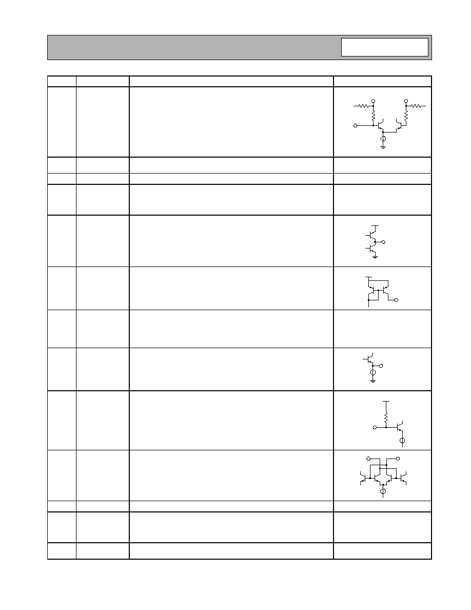
RX IN
LNA OUT
MIX IN
MIX OUT+
V
CC
IF1 IN-
IF1 IN+
330
330
60 k
60 k
IF1 BP+
IF1 BP-
IF1 OUT
11-143
RF2917
Rev B4 021008
NO
T
FOR
N
EW
DE
SI
GNS
Pin
Function
Description
Interface Schematic
16
IF2 IN
Inverting input to the 60dB limiting amplifier strip. A 10 nF DC blocking
capacitor is required on this input. The IF2 IN input presents a nominal
330
input resistance and interfaces directly to 10.7MHz ceramic fil-
ters.
17
IF2 BP+
DC feedback node for the 60dB limiting amplifier strip. A 100nF bypass
capacitor from this pin to ground is required.
See pin 16.
18
IF2 BP-
See pin 17.
See pin 16.
19
VCC3
This pin is used to supply DC bias to the 60dB IF limiting amplifier. An
IF bypass capacitor should be connected directly to this pin and
returned to ground. A 10 nF capacitor is recommended for 10.7MHz IF
applications.
20
MUTE
This pin is used to select FM, FSK, or mute at the FM OUT pin.
MUTE>Vcc - 0.4V turns the FM OUT signal off. MUTE<0.4V turns the
FM OUT signal on for FSK digital data. When MUTE is left floating, the
FM OUT signal is linear FM.
21
RSSI
A DC voltage proportional to the received signal strength is output from
this pin. The output voltage increases with increasing signal strength.
22
FM OUT
Demodulated output from the discriminator/demodulator. Output levels
on this are CMOS compatible in FSK mode (see pin 20). In linear FM
mode, the demodulated signal level is approximately 240mVpp on a
DC voltage offset. The magnitude of the load impedance is intended to
be 1M
or greater.
23
IF2 OUT
IF output from the 60dB limiting amplifier strip. This pin is intended to
be connected to pin 24 through a 5pF capacitor (for 10.7MHz IF appli-
cations). This capacitor in conjunction with a tank resonant at the IF fre-
quency connected from pin 24 to ground is used to form an FM
discriminator.
24
DEMOD IN
This pin is the input to the FM demodulator. This pin is NOT AC cou-
pled. Therefore, a DC blocking capacitor is required on this pin to avoid
a DC path to ground. A DC blocked LC tank resonant at the IF or
ceramic discriminator should be connected to this pin.
25
RESNTR-
This port is used to supply DC voltage to the VCO as well as to tune the
center frequency of the VCO. Equal value inductors should be con-
nected to this pin and pin 26.
26
RESNTR+
See pin 25.
See pin 25.
27
VCC2
This pin is used to supply DC bias to the VCO, prescaler, and PLL. An
IF bypass capacitor should be connected directly to this pin and
returned to ground. A 10nF capacitor is recommended for 10.7MHz IF
applications.
28
GND4
GND4 is the ground shared on chip by the VCO, prescaler, and PLL
electronics.
IF2 IN
330
330
60 k
60 k
IF2 BP+
IF2 BP-
MUTE
V
CC
V
CC
RSSI
IF2 OUT
DEMOD IN
10 k
V
CC
RESNTR
RESNTR+