 | –≠–ª–µ–∫—Ç—Ä–æ–Ω–Ω—ã–π –∫–æ–º–ø–æ–Ω–µ–Ω—Ç: RF3108 | –°–∫–∞—á–∞—Ç—å:  PDF PDF  ZIP ZIP |

¸
2-261
2
PO
W
E
R
A
M
P
LI
FI
E
R
S
Product Description
Ordering Information
Typical Applications
Features
Functional Block Diagram
RF Micro Devices, Inc.
7625 Thorndike Road
Greensboro, NC 27409, USA
Tel (336) 664 1233
Fax (336) 664 0454
http://www.rfmd.com
Optimum Technology MatchingÆ Applied
Si BJT
GaAs MESFET
GaAs HBT
Si Bi-CMOS
SiGe HBT
Si CMOS
PCS IN
VCC
PCS V
APC
GND
GSM V
APC
GSM IN
VCC
GSM OUT
GND
GND
GND
GND
VCC
PCS OUT
14
13
11
12
9
10
8
1
2
4
3
6
5
7
RF3108
TRIPLE-BAND GSM/DCS/PCS
POWER AMP MODULE
∑ 3V Dual-Band/Triple-Band GSM Handsets
∑ Commercial and Consumer Systems
∑ Portable Battery-Powered Equipment
∑ GPRS Compatible
The RF3108 is a high-power, high-efficiency power ampli-
fier module offering high performance in GSM or GPRS
applications. The device is self-contained with 50
input
and output terminals. The device is manufactured on an
advanced GaAs HBT process, and has been designed for
use as the final RF amplifier in GSM/DCS and PCS hand
held-digital cellular equipment and other applications in
the 880MHz to 915MHz and 1710MHz to 1910MHz
bands. On-board power control provides over 70 dB of
control range with an analog voltage input, and provides
power down with a logic "low" for standby operation. The
device is packaged in an ultra-small (9mmx10mm) LCC,
minimizing the required board space.
∑ Single 2.9V to 4.7V Supply Voltage
∑ +35.5dBm GSM Output Pwr at 3.5V
∑ +33.0dBm DCS/PCS Output Pwr at 3.5V
∑ 55% GSM and 50% DCS/PCS Efficiency
∑ Supports GSM, E-GSM and DCS/PCS
∑ 9mmx10mm Package Size
RF3108
Triple-Band GSM/DCS/PCS Power Amp Module
RF3108 PCBA
Fully Assembled Evaluation Board
2
Rev A3 010702
1.40
1.40
1.40
1.40
1.40
1.30
1.40
0.30
10.0 + 0.10
9.0 + 0.10
0.60
typ.
0.90
typ.
Note orientation of Pin 1.
NOTE: Shaded area represents Pin 1.
1.55
+ 0.10
0.38
Ref.
1.00
typ.
Package Style: Module
2-262
RF3108
Rev A3 010702
2
PO
W
E
R
A
M
P
LI
FI
E
R
S
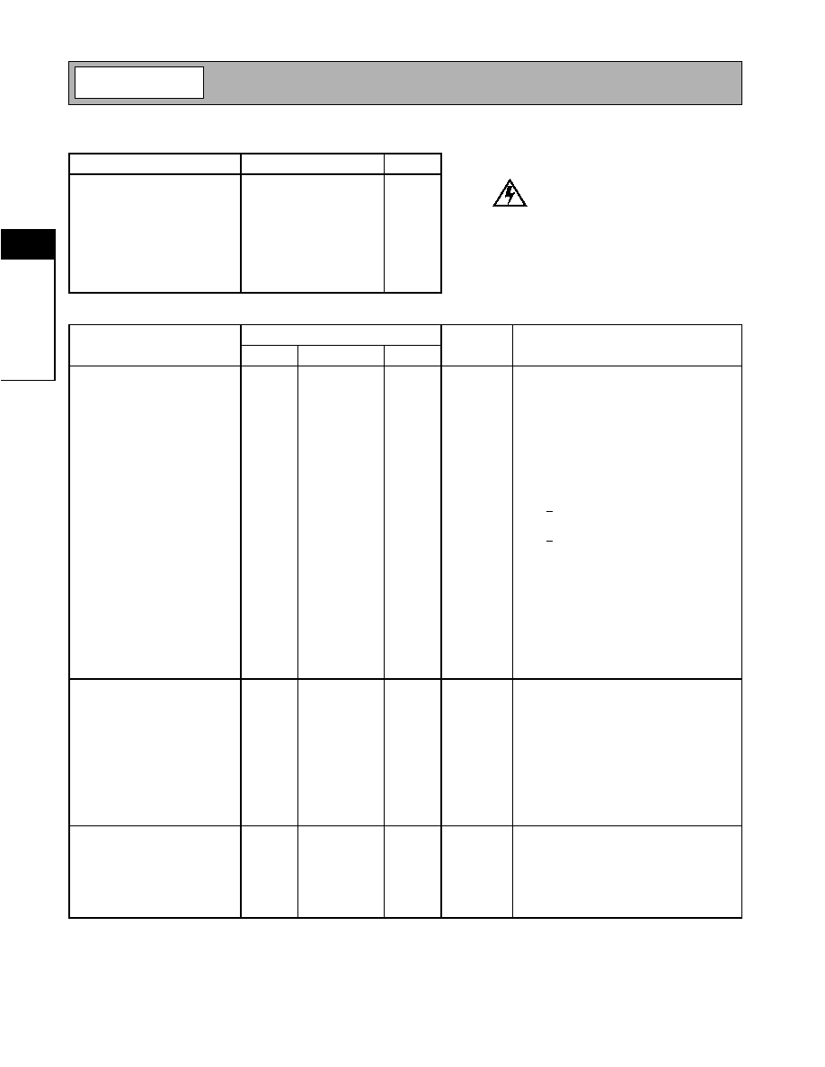
Absolute Maximum Ratings
Parameter
Rating
Unit
Supply Voltage
-0.5 to +6.0
V
DC
Power Control Voltage (V
APC1,2
)
-0.5 to +3.0
V
DC Supply Current
2400
mA
Input RF Power
+13
dBm
Duty Cycle at Max Power
50
%
Output Load VSWR
8:1
Operating Case Temperature
-40 to +85
∞C
Storage Temperature
-55 to +150
∞C
Parameter
Specification
Unit
Condition
Min.
Typ.
Max.
Overall (GSM Mode)
Temp= +25∞C, V
CC
= 3.5V, V
APC GSM
= 2.6V,
P
IN
=6dBm, Freq= 880MHz to 915MHz,
25% Duty Cycle, Pulse Width= 1154
µ
s
Operating Frequency Range
880 to 915
MHz
Maximum Output Power
+34.5
35.5
dBm
Temp = 25∞C, V
CC
= 3.5V, V
APCGSM
=2.6V
+32.0
dBm
Temp= +85 ∞C, V
CC
= 2.9V, V
APCGSM
=2.6V
Total Efficiency
47
55
%
At P
OUT
,
MAX
, V
CC
= 3.5V
Input Power for Max Output
+4
+6
+8
dBm
Output Noise Power
-72
dBm
RBW= 100kHz, 925MHz to 935MHz,
P
OUT
> 34.5dBm
-81
dBm
RBW= 100kHz, 935MHz to 960MHz,
P
OUT
> 34.5dBm
Forward Isolation
-30
dBm
V
APCGSM
=0.2V, PIN= +8dBm
Second Harmonic
-40
-35
dBc
Third Harmonic
-50
-43
dBc
All other non harmonic spurious
-36
dBm
Input Impedance
50
Input VSWR
2.5:1
P
OUT,MAX
-5dB< P
OUT
<P
OUT,MAX
Output Load VSWR
8:1
Spurious<-36dBm, V
APCGSM
= 0.2V to 2.6V,
RBW= 100kHz
Output Load Impedance
50
Load impedance presented at RF OUT pad
Power Control V
APC1
Power Control "ON"
2.6
V
Max. P
OUT
, Voltage supplied to the input
Power Control "OFF"
0.2
0.5
V
Min. P
OUT
, Voltage supplied to the input
Power Control Range
70
dB
V
APC1,2
= 0.2V to 2.6V
Gain Control Slope
100
dB/V
P
OUT
=-10dBm to 35dBm
APC Input Capacitance
10
pF
DC to 2MHz
APC Input Current
4.5
5
mA
V
APC
= 2.6V
10
µ
A
V
APC
=0V
Turn On/Off Time
2
µ
S
V
APC
=0 to 2.6V
Overall Power Supply
Power Supply Voltage
3.5
V
Specifications
2.9
4.7
V
Nominal operating limits, P
OUT
<+33dBm
Power Supply Current
2
A
DC Current at P
OUT,MAX
1
10
µ
A
P
IN
<-30dBm, V
APC1,2
= 0.2V,
Temp= -40to+85 ∞C
Caution! ESD sensitive device.
RF Micro Devices believes the furnished information is correct and accurate
at the time of this printing. However, RF Micro Devices reserves the right to
make changes to its products without notice. RF Micro Devices does not
assume responsibility for the use of the described product(s).
2-263
RF3108
Rev A3 010702
2
PO
W
E
R
A
M
P
LI
FI
E
R
S
Parameter
Specification
Unit
Condition
Min.
Typ.
Max.
Overall (DCS/PCS Mode)
Temp= 25∞C, V
CC
= 3.5V,
V
APCDCS/PCS
= 2.6V, P
IN
=6dBm,
Freq= 1710MHz to 1910MHz,
25% Duty Cycle, Pulse Width= 1154
µ
s
Operating Frequency Range
1710 to 1910
MHz
Maximum Output Power
+32
+33
dBm
Temp= 25∞C, V
CC
= 3.5V,
V
APCDCS/PCS
= 2.6V, 1710MHz to 1785MHz
31.5
32.5
dBm
1850MHz to 1910MHz
29.0
29.5
dBm
Temp= +85∞C, V
CC
= 2.9V, V
APC
=2.6V,
1850MHz to 1910MHz
29.5
30
dBm
1710MHz to 1785MHz
Total Efficiency
45
52
%
At P
OUT,MAX,
V
CC
= 3.5V,
1710MHz to 1785MHz
40
47
%
At P
OUT,MAX,
V
CC
= 3.5V,
1850MHz to 1910MHz
Recommended Input Power
Range
+4
+6
+8
dBm
Output Noise Power
-77
dBm
RBW =100kHz, 1805MHz to 1880MHz and
1930MHz to 1990MHz,
P
OUT
> 34.5dBm, V
CC
= 3.5V
Forward Isolation
-37
-30
dBm
V
APCDCS/PCS
= 0.2V, P
IN
=+8dBm
Second Harmonic
-60
-45
dBc
P
OUT,
= +32.5dBm
Third Harmonic
-65
-50
dBc
All other spurious
-36
dBm
Input Impedance
50
Input VSWR
-
2.5
P
OUT,MAX
-5dB < P
OUT
< P
OUT,MAX
Output Load VSWR
8:1
Spurious <-36dBm,
V
APCDCS/PCS
= 0.2V to 2.6V, RBW = 100kHz
Output Load Impedance
50
Load impedance presented at RF OUT pin
Power Control V
APC 2
Power Control "ON"
2.6
V
Max. P
OUT
, Voltage supplied to the input
Power Control "OFF"
0.2
0.5
V
Min. P
OUT
, Voltage supplied to the input
Power Control Range
62
68
dB
V
APC1,2
= 0.2V to 2.6V, P
IN
=+8dBm
Gain Control Slope
100
dB/V
P
OUT
= -10dBm to +33dBm
APC Input Capacitance
10
pF
DC to 2MHz
APC Input Current
4.5
5
mA
V
APC
= 2.6V
10
µ
A
V
APC
=0V
Turn On/Off TIme
100
ns
V
APC
=0to2.6V
Overall Power Supply
Power Supply Voltage
3.5
V
Specifications
2.9
4.7
V
Nominal operating limits, P
OUT
< +33dBm
Power Supply Current
1.3
A
DC Current at P
OUT,MAX
1
10
µ
A
P
IN
< -30dBm, V
APC1,2
= 0.2V,
Temp= -40to+85∞C

2-264
RF3108
Rev A3 010702
2
PO
W
E
R
A
M
P
LI
FI
E
R
S
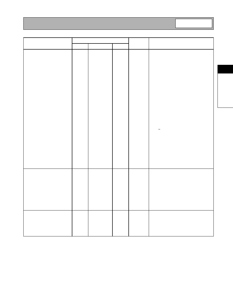
Pin
Function
Description
Interface Schematic
1
VCC1
Power Supply for the driver stage of the DCS/PCS band.
2
DCS/PCS IN
RF Input to the DCS/PCS band. This is a 50
input.
3
DCS/PCS
V
APC
Power control for the pre-amplifier, driver, and output stage of the DCS/
PCS band.
4
GND
Ground connection to overall package.
5
GSM V
APC
Power control for the pre-amplifier, driver, and output stage of the GSM
band.
6
GSM IN
RF input to the GSM band. This is a 50
input.
7
VCC2
Power supply for the driver stage of the GSM band.
8
GSM OUT
RF output for the GSM band. This is a 50
output. The output load line
matching is contained internal to the package.
9
GND
Ground connection to overall package.
10
GND
Ground connection to overall package.
11
VCC3
Power supply for the pre-amplifier and output stage for both the DCS/
PCS and GSM bands.
12
GND
Ground connection to overall package.
13
GND
Ground connection to overall package.
14
DCS/PCS
OUT
RF output for the DCS/PCS band. This is a 50
output. The output
load line matching is contained internal to the package.
Pkg
Base
GND
Ground connection to overall package.

2-265
RF3108
Rev A3 010702
2
PO
W
E
R
A
M
P
LI
FI
E
R
S
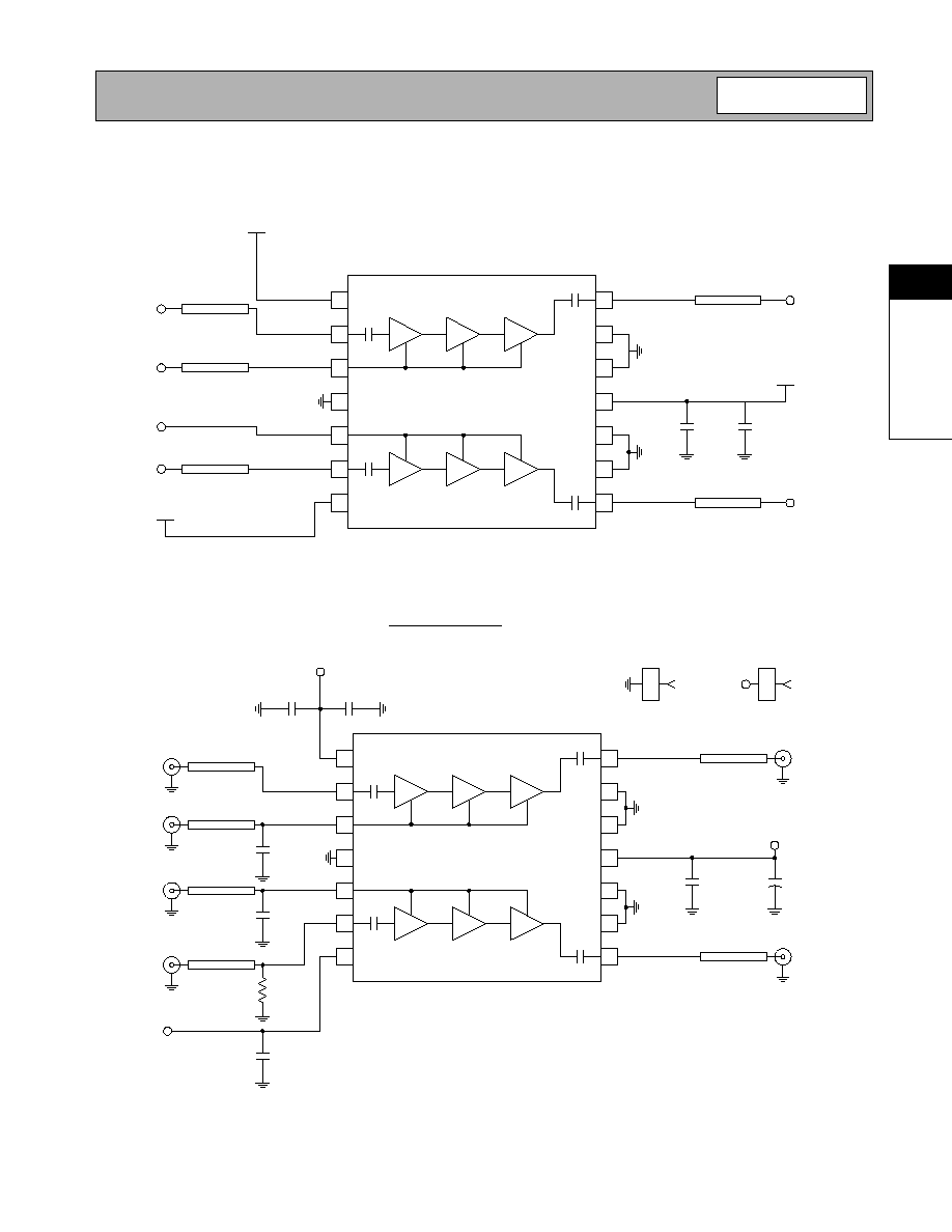
Theory of Operation and Application Information
The RF3108 is a triple-band, GSM/DCS/PCS power
amplifier with two separate RF inputs and outputs that
are internally matched to 50
. Pins 2 and 14 of the
device provide the RF input and output for the DCS/
PCS band, which is optimized for performance
between 1710 MHz and 1910MHz. Pins 5 and 8 of the
device provide the RF input and output for the GSM
band, which is optimized for performance between
880MHz and 915 MHz. Both bands include an internal
DC-blocking capacitor to protect the device from exter-
nal DC source inputs and block internal DC from exit-
ing the inputs and outputs of the module. The
performance is similar to the performance of the
RF2173 and RF2174 MIMIC devices used in dual- or
triple-band applications. However, the RF3108 module
includes the matching and bypass capacitors required
for operation internal to the 9mmx10mm module.
However, some external components are required to
improve stability, isolation and noise power perfor-
mance. These components are included on the evalua-
tion board and schematic, and will be described in the
following paragraphs.
The GSM 900 MHz band provides 32dB and the DCS/
PCS 1710MHz to 1910 MHz band provides 28dB of
small signal gain at full output power. Therefore, the
drive level required to fully saturate the output is
+4dBm for each band. Based upon HBT (Heterojunc-
tion Bipolar Transistor) technology, the part requires
only a single positive 3 V supply to operate to full spec-
ification. The DCS/PCS band input is located at pin 2
of the device and requires no external components.
The GSM 900MHz band input is located at pin 6 of the
device and also does not require external components.
However, a 180
resistor is included at the input of the
GSM band to improve the input impedance and isola-
tion performance at low V
APC
levels. The output for
both high and low bands are internally matched to 50
at the output of pin 14 and 8. A 50
microstrip should
be used to interface to the input and output connec-
tions.
Power control for the GSM 900MHz band is provided
through pin 5 of the device, and pin 3 for the DCS/PCS
band. The V
APC
inputs do not contain any internal
bypass capacitors and will require some external filter-
ing. Because the V
APC
filtering capacitor is external to
the device, the user has the option of choosing a
capacitor value that meets the control loop BW and fil-
tering requirement for various applications. In most typ-
ical applications with a closed loop power control, the
recommended bypass capacitor for this input is
approximately 33pF for the GSM band, and 12pF for
the DCS/PCS band. However in open loop operation, a
10nF V
APC
bypass capacitor is recommended for both
bands to filter noise from the external V
APC
source. A
10nF capacitor is installed on pins 3 and 5 on the cur-
rent evaluation board (see the evaluation board sche-
matic). Noise on the V
APC
input will degrade the noise
power performance of the device, so care should be
used to provide a clean V
APC
input signal. This is espe-
cially important when measuring noise power or stabil-
ity performance.
The voltage supply V
CC
contains internal bypass
capacitors and inductors to filter unwanted noise on
the DC supply voltage. However, the main V
CC
input to
the device at pin 11 requires some additional bypass
capacitors as shown in the evaluation board sche-
matic. C5 (1 uF) and C4 (3.3uF) are required to
improve the stability performance.
All the internal ground connections are connected to a
series of ground pads located on the backside of the
package as shown in the pin out diagram. Pins 4, 9,
10, 12, and 13 are also ground connections. The final
stages of both bands are connected to the ground
pads on the backside of the package. Therefore this
ground connection is essential to dissipate heat and to
provide proper current flow. Refer to the evaluation
board layout as an example of the vias locations and
quantity required for proper connection.
2-266
RF3108
Rev A3 010702
2
PO
W
E
R
A
M
P
LI
FI
E
R
S
Pin Out
7
8
GND
GND
GND
GND
1
14
GND
GND
GND
GND
2
5
3
4
6
13
10
12
11
9
VCC
PCS IN
PCS VAPC
GND
GSM VAPC
GSM IN
VCC
GSM OUT
GND
GND
VCC
GND
GND
PCS OUT
GND
GND
GND
GND
GND
GND
GND
GND
GND
GND
GND
GND
GND
GND
Top View
2-267
RF3108
Rev A3 010702
2
PO
W
E
R
A
M
P
LI
FI
E
R
S
Application Schematic
Evaluation Board Schematic
(Download Bill of Materials from www.rfmd.com.)
1
2
4
3
6
5
7
14
13
11
12
9
10
8
V
CC
50
µ
strip
50
µ
strip
50
µ
strip
V
CC
50
µ
strip
50
µ
strip
DCS/PCS
RF IN
DCS/PCS
VAPC
GSM
VAPC
GSM
RF IN
PCS/DCS
RF OUTPUT
GSM
RF OUTPUT
1
µ
F
V
CC
4.7
µ
F
1
2
4
3
6
5
7
14
13
11
12
9
10
8
50
µ
strip
50
µ
strip
50
µ
strip
50
µ
strip
50
µ
strip
50
µ
strip
J1
DCS/PCS
RF IN
J5
DCS/PCS
VAPC2
J6
GSM
VAPC1
J3
GSM
RF IN
C5
1
µ
F
C7
10 nF
C6
10 nF
R1
180
C4
3.3
µ
F
+
J4
GSM
RF OUTPUT
VCC
J2
PCS/DCS
RF OUTPUT
VCC
VCC
3108400B
C1*
1 nF
C2*
10 nF
C3*
10 nF
Components with (*) following the reference designator
should not be populated on the evaluation board.
GND
P1
1
CON1
P2
1
CON1
P2-1
VCC

2-268
RF3108
Rev A3 010702
2
PO
W
E
R
A
M
P
LI
FI
E
R
S
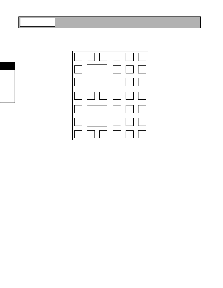
Evaluation Board Layout
Board Size 2.0" x 2.0"
Board Thickness 0.031"; Board Material FR-4; Multi-Layer
2-269
RF3108
Rev A3 010702
2
PO
W
E
R
A
M
P
LI
FI
E
R
S
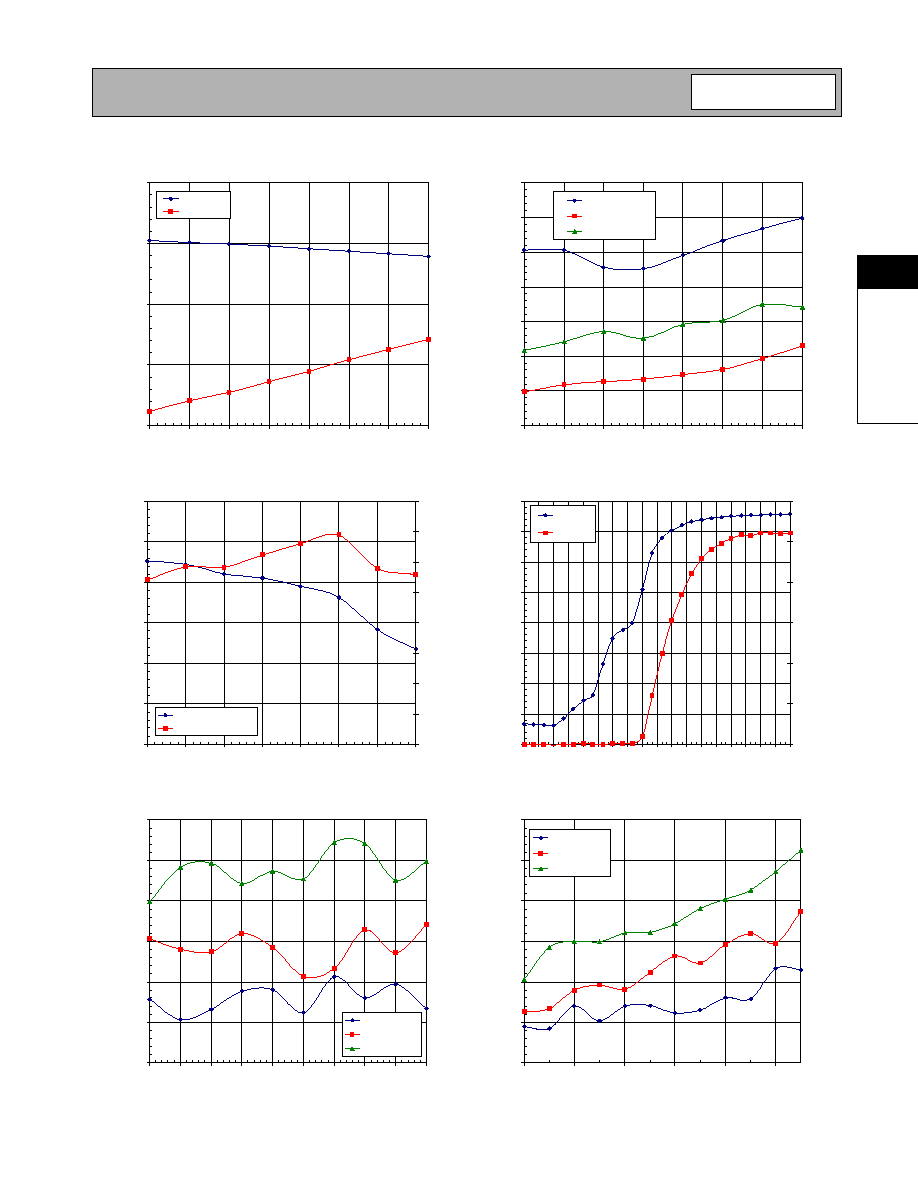
2nd and 3rd Harmonic Performance
GSM Band @3.5V V
CC
, +6dBm P
IN
, 2.6V V
APC
-55.0
-50.0
-45.0
-40.0
-35.0
880.0
885.0
890.0
895.0
900.0
905.0
910.0
915.0
Frequency
Harmonic
Level
(dBc)
2nd Fo(dBc)
3rd Fo(dBc)
Power and Efficiency Performance
@ 3.5V V
CC
, 2.6V V
APC
, +6dBm P
IN
34.8
35.0
35.2
35.4
35.6
35.8
36.0
880.0
885.0
890.0
895.0
900.0
905.0
910.0
915.0
Frequency
Power
(
dBm)
45.0
46.0
47.0
48.0
49.0
50.0
51.0
52.0
53.0
Efficiency
(
%)
Power(+6dBm Pin)
Efficiency (+6dBm Pin)
Power Control Response
@ 3.5V V
CC
, 2.6V V
APC
, +6 dBm P
IN
, 900 MHz
-40.0
-30.0
-20.0
-10.0
0.0
10.0
20.0
30.0
40.0
0.1 0.3 0.4 0.6 0.7 0.9 1.0 1.2 1.3 1.5 1.6 1.8 1.9 2.1 2.2 2.4 2.5 2.7 2.8
Power Control Voltage (V)
Power
(
dBm)
0.0
10.0
20.0
30.0
40.0
50.0
60.0
Efficiency
(
%)
Power
Efficiency
Isolation Performance DCS/PCS Band
@ 3.5V V
CC
, 2.6V
APC
DCS/PCS Band
-39.0
-38.0
-37.0
-36.0
-35.0
-34.0
-33.0
1800.0
1820.0
1840.0
1860.0
1880.0
1900.0
Frequency
Isolation
(
dBm)
Iso@+4dBm Pin
Iso@+6dBm Pin
Iso@+8dBm Pin
Isolation Performance GSM Band
@ 3.5V V
CC
, 2.6V V
APC
-36.0
-35.0
-34.0
-33.0
-32.0
-31.0
-30.0
-29.0
880.0
885.0
890.0
895.0
900.0
905.0
910.0
915.0
Frequency (MHz)
Isolation
(
dBm)
Iso@+8dBm Pin
Iso@+4dBm Pin
Iso@+6dBm Pin
Isolation Performance DCS/PCS Band
@ 3.5V V
CC
, 2.6V
APC
DCS/PCS BAND
-39.0
-38.5
-38.0
-37.5
-37.0
-36.5
-36.0
1700.0 1710.0 1720.0 1730.0 1740.0 1750.0 1760.0 1770.0 1780.0 1790.0
Frequency
Isolation
(
dBm)
Iso@+4dBm Pin
Iso@+6dBm Pin
Iso@+8dBm Pin
2-270
RF3108
Rev A3 010702
2
PO
W
E
R
A
M
P
LI
FI
E
R
S
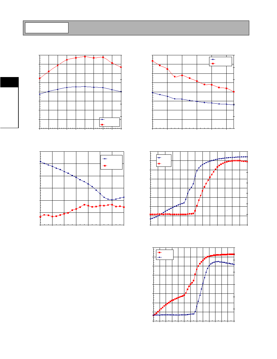
2nd and 3rd Harmonic Performance (DCS/PCS Band)
@ 3.5V V
CC
, +6dBm P
IN
, 2.6V V
APC
-80.0
-75.0
-70.0
-65.0
-60.0
-55.0
-50.0
1700.0
1730.0
1760.0
1790.0
1820.0
1850.0
1880.0
1910.0
Frequency
Harmonic
(
dBc)
2nd Fo(dBc)
3rd Fo(dBc)
PCS Band Power and Efficiency Performance
@ 3.5V V
CC
, 2.6V V
APC
, +8dBm P
IN
31.0
31.5
32.0
32.5
33.0
33.5
34.0
34.5
35.0
1800.0
1820.0
1840.0
1860.0
1880.0
1900.0
Frequency
Power
(
dBm)
39.0
41.0
43.0
45.0
47.0
49.0
51.0
Efficiency
(
%)
Power (dBm)
Efficiency (%)
DCS Band Power and Efficient Performance
@ 3.5V V
CC
, 2.6V V
APC
, +8dBm P
IN
31.0
31.5
32.0
32.5
33.0
33.5
34.0
34.5
35.0
1700.0 1710.0 1720.0 1730.0 1740.0 1750.0 1760.0 1770.0 1780.0 1790.0
Frequency
Power
(
dBm)
40.0
42.0
44.0
46.0
48.0
50.0
52.0
Efficiency
(
%)
Power (dBm)
Efficiency
Power Control Response
@3.5V, 2.6V V
APC
, +6dBm P
IN
, 1750MHz
-40
-30
-20
-10
0
10
20
30
40
0.2
0.4
0.6
0.8
1
1.2
1.4
1.6
1.8
2
2.2
2.4
2.6
2.8
Power Control Voltage (V)
Power
(
dBm)
-
0
1
2
3
4
5
6
Power
Efficiency
Power Control Response
@3.5V V
CC
, 2.6V V
APC
, +6dBm P
IN
, 1850MHz
-40.0
-30.0
-20.0
-10.0
0.0
10.0
20.0
30.0
40.0
0.2
0.4
0.6
0.8
1.0
1.2
1.4
1.6
1.8
2.0
2.2
2.4
2.6
2.8
Power Control Voltage (V)
Power
(
dBm)
0.0
10.0
20.0
30.0
40.0
50.0
60.0
Efficiency
(
%)
Power
Efficiency