
2-1
3
LI
N
E
A
R
C
A
TV
A
M
P
L
IF
IE
R
S
Preliminary
Product Description
Ordering Information
Typical Applications
Features
Functional Block Diagram
RF Micro Devices, Inc.
7628 Thorndike Road
Greensboro, NC 27409, USA
Tel (336) 664 1233
Fax (336) 664 0454
http://www.rfmd.com
Optimum Technology Matching� Applied
Si BJT
GaAs MESFET
GaAs HBT
Si Bi-CMOS
�
SiGe HBT
Si CMOS
1
2
3
4
5
6
7
8
16
15
14
13
12
11
10
9
SHDNB
TX EN
NC
VIN
VINB
VCC1
VCC1
RAMP
GND
NC
NC
VOUT
VOUTB
SDA
CS
SCLK
Power
Control
Gain Control
and Serial Bus
RF3321
REVERSE PATH HIGH OUTPUT POWER
PROGRAMMABLE GAIN AMPLIFIER
� Euro-DOCSIS/DOCSIS Cable Modems
� CATV Set-Top Boxes
� Telephony Over Cable
� Home Networks
� Automotive/Mobile Multimedia
� Coaxial and Twisted Pair Line Driver
The RF3321 is a variable gain amplifier for use in CATV
reverse path (upstream) applications. It is designed to be
DOCSIS-compliant for use in cable modems. The gain
control covers a 56 dB range and is serially programma-
ble via three-wire digital bus for compatibility with stan-
dard baseband chipsets. Amplifier shutdown and transmit
disable modes are hardware-controlled. The device oper-
ates over the frequency band of 5MHz to 65MHz for use
in current U.S. and European systems. The amplifier
delivers up to +69dBmV at the output of the balun. Gain
is controllable in accurate 1dB steps. The device is pro-
vided in a thermally enhanced, exposed die flag package.
� Differential Input and Output
� 31dB Maximum Voltage Gain
� -25dB Minimum Voltage Gain
� 5MHz to 65MHz Operation
� Sophisticated Power Management
� DOCSIS 1.1 RF Compliant
RF3321
Reverse Path High Output Power Programmable
Gain Amplifier
RF3321 PCBA
Fully Assembled Evaluation Board
2
Rev A10 010516
NOTES:
1. Shaded lead is pin 1.
2. Lead coplanarity - 0.10 with
respect to datum "A".
3. Lead standoff is specified from
the lowest point on the package
underside.
8� MAX
0� MIN
0.60
+ 0.15
0.24
0.20
3.90
+ 0.10
0.25
+ 0.05
0.65
6.00
+ 0.20
4.90
+ 0.20
EXPOSED DIE
FLAG
3.302
2.286
1.40
+ 0.10
0.05
+ 0.05
Note 3
-A-
Package Style: SSOP16 EDF Slug

Preliminary
2-2
RF3321
Rev A10 010516
3
LI
N
E
A
R
C
A
TV
A
M
P
L
IF
IE
R
S
Absolute Maximum Ratings
Parameter
Rating
Unit
Supply Voltage (V
CC1
)
-0.5 to +5.5
V
DC
Supply Voltage (V
CC2
)
-0.5 to +7.5
V
DC
Input RF Level
12
dBm
Operating Ambient Temperature
-40 to +85
�C
Storage Temperature
-40 to +150
�C
Humidity
80
%
Maximum Power Dissipation
0.5
W
Maximum T
J
150
�C
Parameter
Specification
Unit
Condition
Min.
Typ.
Max.
Overall
V
CC1
=5V, V
CC2
=7V, TXEN=SHDNB=1,
V
IN
=38dBmV (rms) differential, output
impedance= 75
through a 2:1 transformer.
Typical performance is at T
A
= +25�C,
V
CC
=5V.
DC Specifications
Supply Voltage 1 (VCC1)
4.75
5.0
5.25
V
Main chip supply
Supply Voltage 2 (VCC2)
6.65
7.0
7.35
V
Output stage supply
Supply Current
Maximum Gain, SV1
85
100
mA
Gain Control Word= 56, V
CC2
=5V or 7V
Maximum Gain, SV2
135
150
mA
Gain Control Word= 56, V
CC2
=5V or 7V
Low Gain, SV1
75
90
mA
Gain Control Word< 28, V
CC2
=5V or 7V
Low Gain, SV2
55
70
mA
Gain Control Word< 28, V
CC2
=5V or 7V
Transmit Disable
25
35
mA
TXEN=0, V
CC2
= 5V or 7V
Shut Down
5
mA
SHDNB= 0, V
CC2
=5V or 7V
Logic High Voltage
2
V
Logic Low Voltage
0.8
V
Logic Leakage Current
-1
1
�
A
AC Specifications
Voltage Gain
Maximum
29
31
dB
Gain Control Word= 56, V
CC2
=5V or 7V
Minimum
-25
-23
dB
Gain Control Word= 0, V
CC2
=5V or 7V
Bandwidth
100
MHz
Intended operating range is 5MHz to
65MHz.
Maximum Input Level
40
dBmV(rms)
Maximum Output Level
69
dBmV(rms)
Into 75
load at balun output (CW),
V
CC2
=7V
65
dBmV
V
CC2
=5V
Output Harmonic Distortion
-56
-50
dBc
Output Level= 68dBmV (rms) (CW)
Maximum Gain, V
CC2
=5V or 7V
Output Step Size
0.8
1.0
1.1
dB
Output Noise
Maximum Gain
-35
-30
dBmV/
160kHz
V
CC2
=5V or 7V
Minimum Gain
-50
-45
dBmV/
160kHz
V
CC2
=5V or 7V
Transmit Disabled
-75
-70
dBmV/
160kHz
TXEN= 0, V
CC2
= 5V or 7V
TX EN Enable Time
0.5
1.0
�
S
Time for gain to reach 99% of final value.
See Note 1.
TX EN Transient Duration
2.4
3.0
�
S
See Note 1.
Caution! ESD sensitive device.
RF Micro Devices believes the furnished information is correct and accurate
at the time of this printing. However, RF Micro Devices reserves the right to
make changes to its products without notice. RF Micro Devices does not
assume responsibility for the use of the described product(s).
Preliminary
2-3
RF3321
Rev A10 010516
3
LI
N
E
A
R
C
A
TV
A
M
P
L
IF
IE
R
S
Note 1: The enable time is determined by the value of the capacitor on pin 8 (RAMP). A higher capacitor value will
increase the enable time, but will reduce the transient voltage
.
Parameter
Specification
Unit
Condition
Min.
Typ.
Max.
AC Specifications, cont'd
Output Switching Transients
Maximum Gain
10
20
mV
P-P
Minimum Gain
5
7
mV
P-P
Output Impedance
300
Chip output impedance is nominally 300
.
Differential to single-ended output conver-
sion to 75
is performed in a balun with a
2:1 turns ratio, corresponding to a 4:1 imped-
ance ratio.
Input Impedance
75
Differential
Thermal
Theta
JC
28
�C/W

Preliminary
2-4
RF3321
Rev A10 010516
3
LI
N
E
A
R
C
A
TV
A
M
P
L
IF
IE
R
S
Serial Bus Block Diagram
Pin
Function
Description
Interface Schematic
1
SHDNB
Chip shutdown pin. Forcing a logic low causes all circuits to switch off
and gain settings to be lost.
2
TX EN
Signal path enable pin. Logic high turns on signal path. Logic low turns
off signal path, but leaves serial bus active.
3
NC
Not connected.
4
VIN
Input pin. This should be externally AC-coupled to signal source.
5
VINB
Complementary input pin. This should be externally coupled to signal
source. For single-ended use, this pin should be AC-coupled to ground.
See pin 4.
6
VCC1
This pin is connected to VCC1.
7
VCC1
Same as pin 6.
8
RAMP
External capacitor to ground controls start-up time.
9
SCLK
Serial bus clock input.
10
CS
Serial bus enable.
11
SDA
Serial bus data input.
12
VOUTB
Open collector output. Connect to VCC2 via balun primary.
13
VOUT
Open collector output. Connect to VCC2 via balun primary.
See pin 12.
14
NC
Same as pin 3.
15
NC
Same as pin 3.
16
GND
Connect to ground.
PKG
BASE
GND
Die is mounted on a heat sink slug that should be connected to ground.
Device grounds are internally bonded to the slug.
550
550
V
CC
500
500
V
INB
V
IN
300
V
OUT
V
OUTB
RE
D
CK
Q
CLR
D
CK
Q
CLR
D
CK
Q
CLR
D
CK
Q
CLR
D
CK
Q
CLR
D
CK
Q
CLR
D
CK
Q
CLR
D
CK
Q
CLR
D
CK
Q
CLR
D
CK
Q
CLR
D
CK
Q
CLR
D
CK
Q
CLR
D
CK
Q
CLR
D
CK
Q
CLR
D0
D1
D2
D3
D4
D5
D6
POR
CS
SDA
SCLK

Preliminary
2-5
RF3321
Rev A10 010516
3
LI
N
E
A
R
C
A
TV
A
M
P
L
IF
IE
R
S
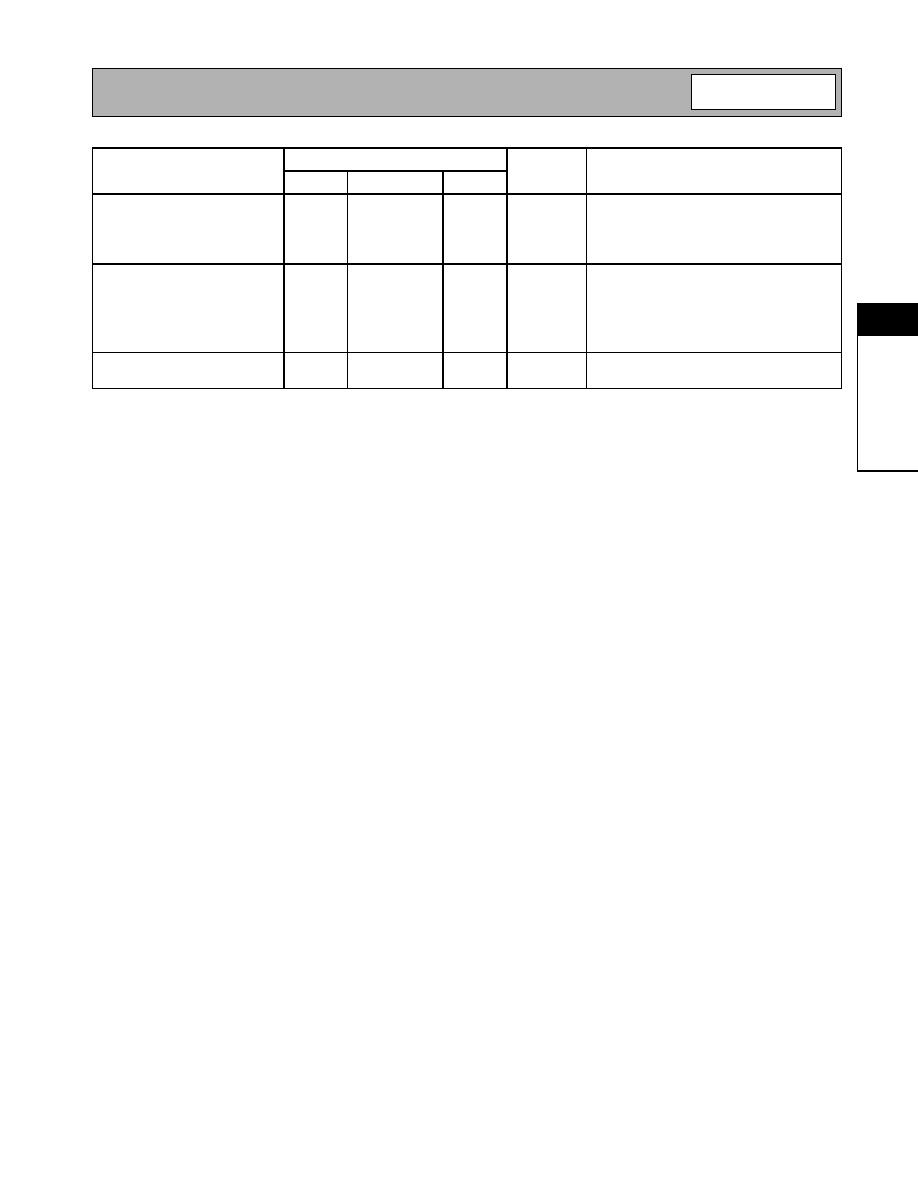
Table 1. Serial Interface Control Word Format
Serial Bus Timing Diagram
Table 2. Timing Data
Table 3. Programming State
Bit
Mnemonic
Description
MSB 6
D6
Sleep Mode (Software Shutdown)
5
D5
Gain Control, Bit MSB
4
D4
Gain Control, Bit 4
3
D3
Gain Control, Bit 3
2
D2
Gain Control, Bit 2
1
D1
Gain Control, Bit 1
LSB 0
D0
Gain Control, Bit LSB
Parameter
Symbol
Min
Typ
Max
Units
SCLK Pulsewidth
T
WH
50
ns
SCLK Period
T
C
100
ns
Setup Time, SDA versus S CLK
T
DS
10
ns
Setup Time, CS versus S CLK
T
ES
10
ns
Hold Time, SDA versus S CLK
T
DH
20
ns
Hold Time, CS versus S CLK
T
EH
20
ns
SCLK Pulsewidth, High
T
DATAH
50
ns
SCLK Pulsewidth, Low
T
DATAL
50
ns
TX
SHDND
MSB6
Enter Sleep Mode
X
H
L
H= High Voltage Logic
Exit Sleep Mode
X
H
H*
L=Low Voltage Logic
Enter Shutdown
X
L
X
X =Don't Care
Exit Shutdown
X
H
H*
*Gain Control Data Must be Re-Sent
TX Enable
H
X
X
TX Disable
L
X
X
D0
D1
D2
D3
D4
D5
D6
T
ES
T
DS
T
DH
T
EH
T
WH
T
C
T
DATAH
,T
DATAL
CS
SCLK
SDA
(Data)