 | –≠–ª–µ–∫—Ç—Ä–æ–Ω–Ω—ã–π –∫–æ–º–ø–æ–Ω–µ–Ω—Ç: RF5107 | –°–∫–∞—á–∞—Ç—å:  PDF PDF  ZIP ZIP |

2-561
Product Description
Ordering Information
Typical Applications
Features
Functional Block Diagram
RF Micro Devices, Inc.
7628 Thorndike Road
Greensboro, NC 27409, USA
Tel (336) 664 1233
Fax (336) 664 0454
http://www.rfmd.com
Optimum Technology MatchingÆ Applied
Si BJT
GaAs MESFET
GaAs HBT
Si Bi-CMOS
SiGe HBT
Si CMOS
InGaP/HBT
GaN HEMT
SiGe Bi-CMOS
RF OUT
RF OUT
RF OUT
2F
0
V
C
C BI
AS
VCC1
VCC1
GND
RF IN
VR
EG
1
VMODE
VR
EG
2
B
I
AS
GND
16
15
14
13
12
11
10
9
5
6
7
8
1
2
3
4
GND
GND
GND
RF5107
3V 900MHZ LINEAR AMPLIFIER
∑ 3V CDMA/AMPS Cellular Handsets
∑ Spread-Spectrum Systems
The RF5107 is a high-power, high-efficiency linear ampli-
fier IC targeting 3V handheld systems. The device is
manufactured on an advanced Gallium Arsenide Hetero-
junction Bipolar Transistor (HBT) process, and has been
designed for use as the final RF amplifier in dual-mode
3V CDMA/AMPS handheld digital cellular equipment,
spread-spectrum systems, and other applications in the
800MHz to 960MHz band. The RF5107 has a low power
mode to extend battery life under low output power condi-
tions. The RF5107 is assembled in a 16-pin, 3mmx3mm
QFN package.
∑ Single 3V Supply
∑ 29dBm Linear Output Power
∑ Low Power Mode
∑ 37% Linear Efficiency
∑ 50mA Idle Current
∑ Gain Control
RF5107
3V 900MHz Linear Amplifier
RF5107 PCBA
Fully Assembled Evaluation Board
0
Rev B1 030512
0.90
0.85
0.05 C
0.05
0.00
0.70
0.65
12∞
MAX
-C-
SEATING
PLANE
1.50 TYP
0.10 C A
2 PLCS
-A-
3.00
0.10 C B
2 PLCS
1.37 TYP
0.10 C A
2 PLCS
2.75 SQ
0.10 C B
2 PLCS
3.00
-B-
0.60
0.24
TYP
0.50
0.30
PIN 1 ID
R.20
0.50
1.65
1.35
SQ.
0.10
C A B
M
0.30
0.18
2
NOTES:
1. Shaded lead is pin 1.
Dimension applies to plated terminal: to be measured
between 0.20 mm and 0.25 mm from terminal end.
2
Dimensions in mm.
Package Style: QFN, 16-Pin, 3x3
!

2-562
RF5107
Rev B1 030512
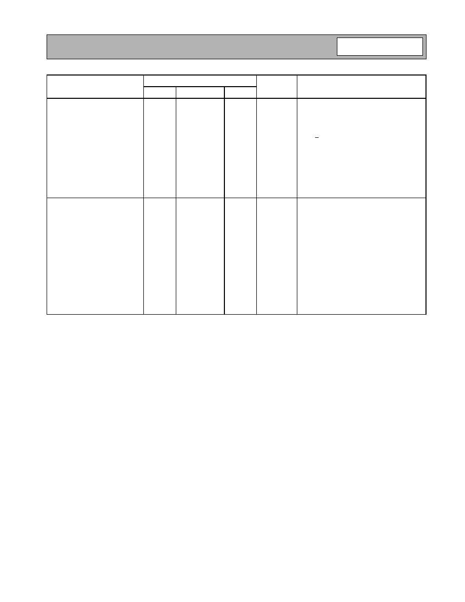
Absolute Maximum Ratings
Parameter
Rating
Unit
Supply Voltage (RF off)
+8.0
V
DC
Supply Voltage (P
OUT
31dBm)
+5.2
V
DC
Mode Voltage (V
MODE
)
+4.2
V
DC
Control Voltage (V
REG
)
+3.0
V
DC
Input RF Power
+10
dBm
Operating Case Temperature
-30 to +110
∞C
Storage Temperature
-30 to +150
∞C
Parameter
Specification
Unit
Condition
Min.
Typ.
Max.
High Power State
(V
MODE
Low)
Ambient T=25∞C, V
CC
=3.4V, V
REG
=2.85V,
V
MODE
=0V to 0.5V, Freq=824MHz to
849MHz (unless otherwise specified)
Frequency Range
824
849
MHz
Linear Gain
27
30
dB
Second Harmonic
-30
-25
dBc
Third Harmonic
-40
-37
dBc
Maximum Linear Output Power
(CDMA Modulation)
29
dBm
Total Linear Efficiency
37
%
P
OUT
=29dBm
Adjacent Channel Power Rejec-
tion
-46
-44
dBc
ACPR@885kHz
-58
-56
dBc
ACPR@1980kHz
Input VSWR
2:1
Output VSWR
10:1
No damage.
6:1
No oscillations. >-70dBc
Noise Power
-133
dBm/Hz
At 45MHz offset.
Low Power State
(V
MODE
High)
Ambient T=25∞C, V
CC
=3.4V, V
REG
=2.85V,
V
MODE
=1.8V to 3V, Freq=824MHz to
849MHz (unless otherwise specified)
Frequency Range
824
849
MHz
Linear Gain
19
22
25
dB
Second Harmonic
-30
-25
dBc
Third Harmonic
-40
-37
dBc
Maximum Linear Output Power
(CDMA Modulation)
16
dBm
Max I
CC
200
mA
P
OUT
=+16dBm (all currents included)
Adjacent Channel Power Rejec-
tion
-44
dBc
ACPR@885kHz
-56
dBc
ACPR@1980kHz
Input VSWR
2:1
Output VSWR
10:1
No damage.
6:1
No oscillations. >-70dBc
Caution! ESD sensitive device.
RF Micro Devices believes the furnished information is correct and accurate
at the time of this printing. However, RF Micro Devices reserves the right to
make changes to its products without notice. RF Micro Devices does not
assume responsibility for the use of the described product(s).
2-563
RF5107
Rev B1 030512
Parameter
Specification
Unit
Condition
Min.
Typ.
Max.
FM Mode
Ambient T=25∞C, V
CC
=3.4V, V
REG
=2.85V,
V
MODE
=0V to 0.5V, Freq=824MHz to
849MHz (unless otherwise specified)
Frequency Range
824
849
MHz
Gain
26
30
dB
P
OUT
<31dBm
Second Harmonic
-30
-25
dBc
Third Harmonic
-40
-37
dBc
Max CW Output Power
31
32
dBm
Total Efficiency (AMPS mode)
45
%
P
OUT
=31dBm (room temperature)
Input VSWR
2:1
Output VSWR
10:1
No damage.
6:1
No oscillations. >-70dBc
DC Supply
Supply Voltage
3.0
3.4
4.2
V
Quiescent Current
120
160
200
mA
V
CC
=3.4V, V
REG
=2.85V, V
MODE
= Low
50
80
mA
V
CC
=3.4V, V
REG
=2.85V, V
MODE
= High
V
REG
Current
10
mA
V
MODE
Current
1
mA
Turn On/Off Time
40
µ
s
Time between V
REG
turned on and part
reaching full power.
Total Current (Power Down)
10
µ
A
V
REG
=Low
V
REG
"Low" Voltage
0
0.5
V
V
REG
"High" Voltage
2.75
2.85
2.95
V
V
MODE
"Low" Voltage
0
0.5
V
V
MODE
"High" Voltage
1.8
3.0
V
2-564
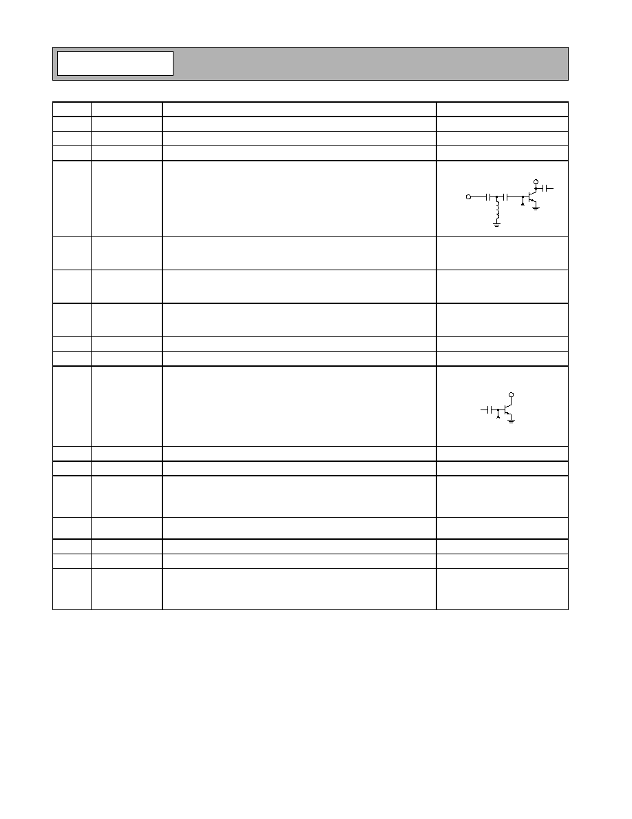
RF5107
Rev B1 030512
Pin
Function
Description
Interface Schematic
1
GND
Ground connection.
2
GND
Ground connection.
3
GND
Ground connection.
See pin 10.
4
RF IN
RF input. An external 100pF series capacitor is required as a DC block.
In addition, shunt inductor and series capacitor are required to provide
2:1VSWR.
5
VREG1
Power Down control for first stage. Regulated voltage supply for ampli-
fier bias. In Power Down mode, both V
REG
and V
MODE
need to be LOW
(<0.5V).
6
VMODE
For nominal operation (High Power Mode), V
MODE
is set LOW. When
set HIGH, the driver and final stage are dynamically scaled to reduce
the device size and as a result to reduce the idle current.
7
VREG2
Power Down control for the second stage. Regulated voltage supply for
amplifier bias. In Power Down mode, both V
REG
and V
MODE
need to be
LOW (<0.5V).
8
BIAS GND
Bias circuitry ground. See application schematic.
9
GND
Ground connection.
10
RF OUT
RF output and power supply for final stage. This is the unmatched col-
lector output of the second stage. A DC block is required following the
matching components. The biasing may be provided via a parallel L-C
set for resonance at the operating frequency of 824MHz to 849MHz. It
is important to select an inductor with very low DC resistance with a 1A
current rating. Alternatively, shunt microstrip techniques are also appli-
cable and provide very low DC resistance. Low frequency bypassing is
required for stability.
11
RF OUT
Same as pin 10.
See pin 10.
12
RF OUT
Same as pin 10.
See pin 10.
13
2FO
Harmonic trap. This pin connects to the RF output but is used for pro-
viding a low impedance to the second harmonic of the operating fre-
quency. An inductor or transmission line resonating with an on chip
capacitor at 2fo is required at this pin.
14
VCC BIAS
Power supply for bias circuitry. A 100pF high frequency bypass capaci-
tor is recommended.
15
VCC1
Power supply for the first stage.
16
VCC1
Same as pin 15.
Pkg
Base
GND
Ground connection. The backside of the package should be soldered to
a top side ground pad which is connected to the ground plane with mul-
tiple vias. The pad should have a short thermal path to the ground
plane.
GND1
RF IN
VCC1
From
Bias
Stages
100 pF
RF OUT
From Bias
Stages
2-565
RF5107
Rev B1 030512
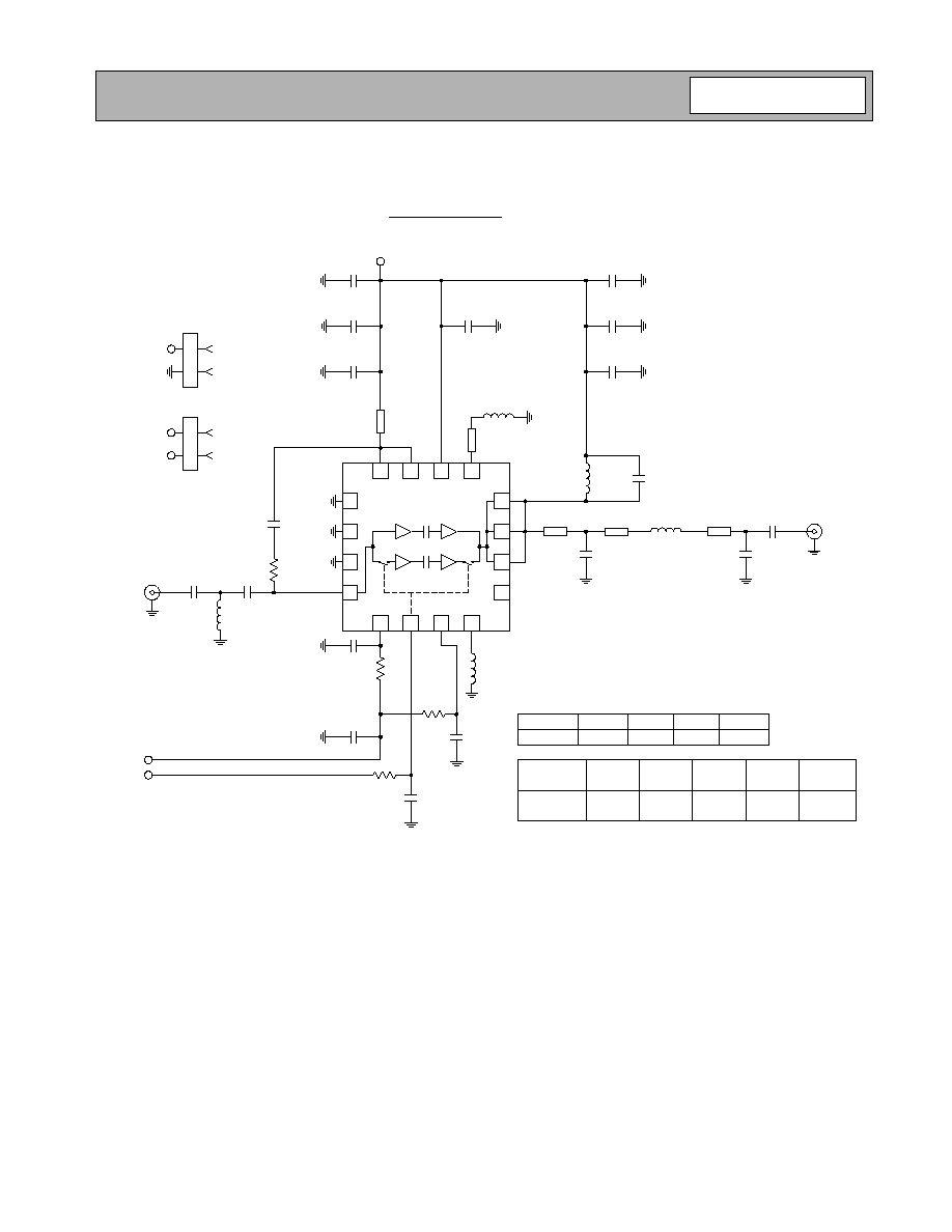
Evaluation Board Schematic
US - CDMA
(Download Bill of Materials from www.rfmd.com.)
C4
4.7
µ
F
C30
C21
100 pF
C7
100 pF
R1
0
C15
100 pF
C1**
C14**
C5
100 pF
L1*
C8
100 pF
C9
10 nF
C6
4.7 uF
C12
2.4 pF
R2
0
C10
4.7
µ
F
* L1 is a High Q inductor (i.e., Coilcraft 0805HQ-series).
**C1 and C14 are High Q capacitors
(i.e., Johanson C-series).
L2
39 nH
R3
0
L4
5.6 nH
J1
RF IN
VCC
L3
1.5 nH
J4
RF OUT
P1
1
2
P1-1
VCC
GND
P2
1
2
P2-1
VREG
VMODE
P2-2
VREG
VMODE
TL
5
C16
12 pF
CDMA (US)
470
10
20
9.1
Board
C30 (pF) C1 (pF) L1 (nH) C14 (pF)
TL
1
TL
2
C20
100 pF
R4
510
C17
100 pF
C11
4.7
µ
F
TL
4
125-135
mils
TL
5
100 mils
TL
3
70 mils
TL
2
80 mils
TL
1
55-65
mils
Transmission
Line Length
CDMA (US)
L5
1 nH
TL
4
C13
100 pF
TL
3
16
15
14
13
12
11
10
9
5
6
7
8
1
2
3
4