 | –≠–ª–µ–∫—Ç—Ä–æ–Ω–Ω—ã–π –∫–æ–º–ø–æ–Ω–µ–Ω—Ç: RF5176 | –°–∫–∞—á–∞—Ç—å:  PDF PDF  ZIP ZIP |

¸
2-197
2
PO
W
E
R
A
M
P
LI
FI
E
R
S
Preliminary
Product Description
Ordering Information
Typical Applications
Features
Functional Block Diagram
RF Micro Devices, Inc.
7628 Thorndike Road
Greensboro, NC 27409, USA
Tel (336) 664 1233
Fax (336) 664 0454
http://www.rfmd.com
Optimum Technology MatchingÆ Applied
Si BJT
GaAs MESFET
GaAs HBT
Si Bi-CMOS
SiGe HBT
Si CMOS
VREG1
VCC BIAS
VREG2
VS2
BIAS GND
RF
O
U
T
NC
NC
RF
O
U
T
RF
O
U
T
VCC1
VCC1
NC
NC
NC
Q1B
NC
RF
I
N
NC
NC
5
6
7
8
9
10
11
12
4
3
2
1
16
15
14
13
20
19
18
17
Bia
s
RF5176
3V W-CDMA POWER 1900MHZ/
3V LINEAR POWER AMPLIFIER
∑ 3V 1850-1910MHz CDMA-2000 Handsets
∑ 3V 1920-1980MHz W-CDMA Handsets
∑ Spread-Spectrum Systems
∑ Commercial and Consumer Systems
∑ Portable Battery-Powered Equipment
The RF5176 is a high-power, high-efficiency linear ampli-
fier IC targeting 3V handheld systems. The device is
manufactured on an advanced Gallium Arsenide Hetero-
junction Bipolar Transistor (HBT) process, and has been
designed for use as the final RF amplifier in 3V
CDMA-2000 and W-CDMA handsets as well as other
applications in the 1850MHz to 2000MHz band. The
device is self-contained, and the output can be easily
matched to obtain optimum power, efficiency, and linear-
ity characteristics over all recommended supply voltages.
The device has a continuously variable bias circuit to
allow idle current to be optimized for a given output
power.
∑ Single 3V Supply
∑ 27dBm Linear Output Power
∑ 26dB Linear Gain
∑ 40% Linear Efficiency
∑ On-board Power Down Mode
RF5176
3V W-CDMA Power 1900MHZ/ 3V Linear Power
Amplifier
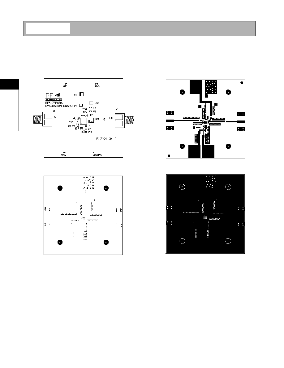
RF5176 PCBA
Fully Assembled Evaluation Board
2
Rev A0 010910
1.00
0.90
4.00
sq.
0.60
0.24 typ
3
0.20
0.75
0.50
0.23
0.13
4 PLCS
0.50
2.10
sq.
0.65
0.30
4 PLCS
0.05
12∞
MAX
Dimensions in mm.
Note orientation of package.
NOTES:
Package Warpage: 0.05 mm max.
4
Die Thickness Allowable: 0.305 mm max.
5
Pin 1 identifier must exist on top surface of package by identification
mark or feature on the package body. Exact shape and size is optional.
2
Shaded lead is Pin 1.
1
Dimension applies to plated terminal: to be measured between 0.02 mm
and 0.25 mm from terminal end.
3
Package Style: LCC, 20-Pin, 4x4

Preliminary
2-198
RF5176
Rev A0 010910
2
PO
W
E
R
A
M
P
LI
FI
E
R
S
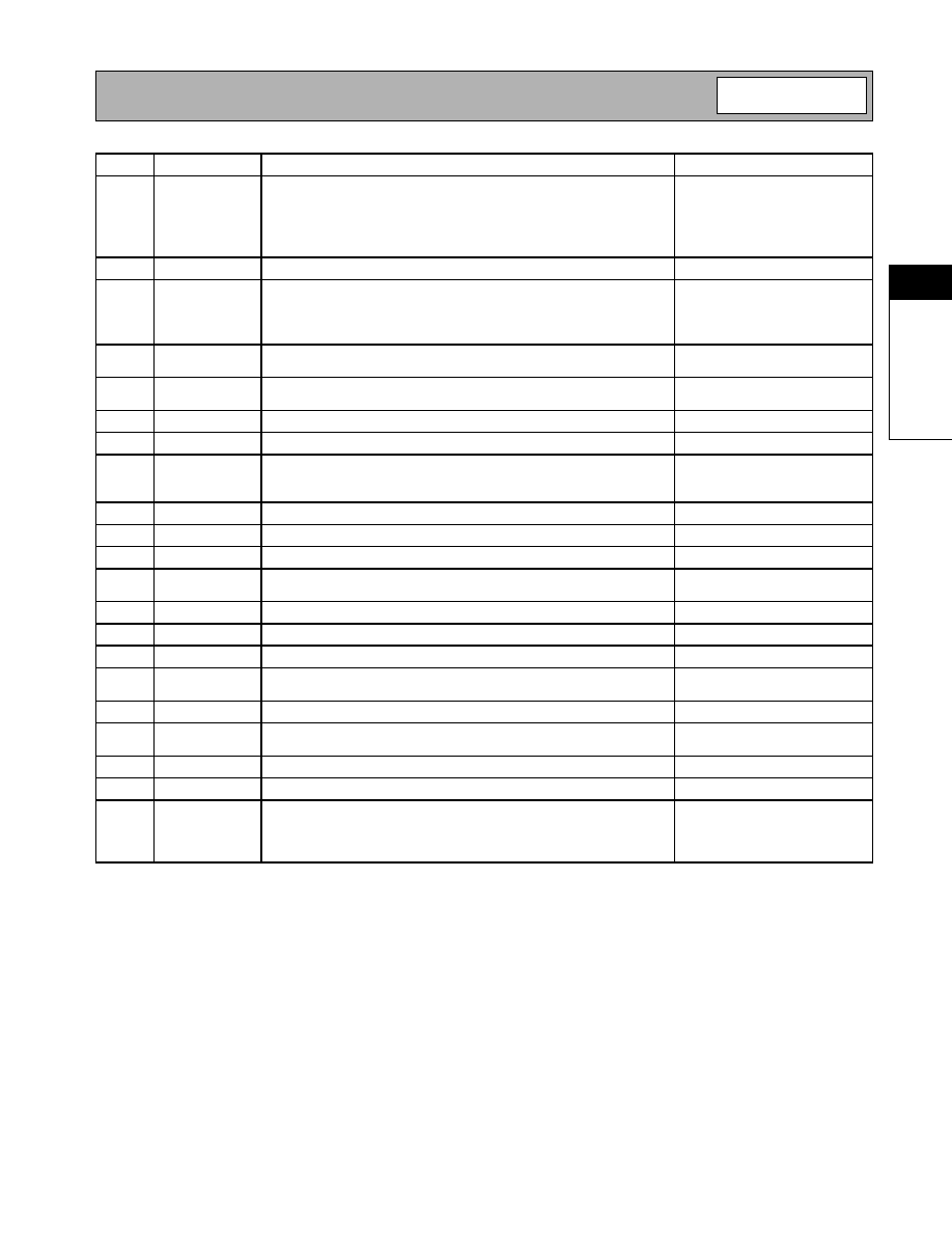
Absolute Maximum Ratings
Parameter
Rating
Unit
Supply Voltage (RF off)
+8.0
V
DC
Supply Voltage (P
OUT
31dBm)
+5.0
V
DC
Bias Voltage (V
BIAS
)
+3.0
V
DC
Control Voltage (V
REG
)
+3.0
V
DC
Input RF Power
+6
dBm
Operating Case Temperature
-30 to +100
∞C
Storage Temperature
-30 to +150
∞C
Parameter
Specification
Unit
Condition
Min.
Typ.
Max.
Overall
T = 25∞C, V
CC
= 3.4V,
Freq= 1920MHz to 1980MHz, V
REG
= 2.5V,
unless otherwise specified
Usable Frequency Range
1850
2000
MHz
Typical Frequency Range
1850 to 1910
MHz
1920 to 1980
MHz
Linear Gain
26
dB
Second Harmonic (including
second harmonic trap)
-55
dBc
Third Harmonic
-50
dBc
Maximum Linear Output Power
(W-CDMA Modulation)
27
dBm
Total Linear Efficiency
40
%
P
OUT
=27dBm
Adjacent Channel Power
Rejection@5MHz
-40
-38
dBc
P
OUT
=27dBm, W-CDMA Modulation,
3GPP 3.2 03-00 DPCCH + 1 DPDCH
Adjacent Channel Power
Rejection@10MHz
-50
-48
dBc
P
OUT
=27dBm, W-CDMA Modulation,
3GPP 3.2 03-00 DPCCH + 1 DPDCH
Noise Power
-144
dBm/Hz
P
OUT
=+27dBm,
Rx Band 2110MHz to 2170MHz
Input VSWR
< 2:1
Output Load VSWR
5:1
No oscillations
Power Supply
Power Supply Voltage
3.0
3.4
5.0
V
Idle Current
80
mA
V
REG
=2.5V
VREG Current
10
µ
A
Total pins 1 and 3, V
REG
= 2.5V
Turn On/Off time
ns
Total Current (Power down)
10
µ
A
V
REG
=Low
V
REG
"Low" Voltage
0
0.2
V
V
REG
"High" Voltage
2.5
V
See Alternative Biasing Network table follow-
ing the application schematic.
Caution! ESD sensitive device.
RF Micro Devices believes the furnished information is correct and accurate
at the time of this printing. However, RF Micro Devices reserves the right to
make changes to its products without notice. RF Micro Devices does not
assume responsibility for the use of the described product(s).
Preliminary
2-199
RF5176
Rev A0 010910
2
PO
W
E
R
A
M
P
LI
FI
E
R
S
Pin
Function
Description
Interface Schematic
1
VREG1
Bias control for the first stage. Needs to be divided down from its nomi-
nal value of 2.5V using a resistive divider network of 240k
and
360k
. V
REG1
and V
REG2
may be adjusted to minimize idle current for
a given output power. Alternative V
REG
voltages can be used as
defined on the application schematic.
2
VCC BIAS
Supply for bias circuits.
3
VREG2
Bias control for the second stage. Needs to be divided down from its
nominal value of 2.5V using a resistive divider network of 240k
and
240k
. Alternative V
REG
voltages can be used as defined on the appli-
cation schematic.
4
VS2
Second stage bias circuit source. For best linearity, decouple with
bypassing capacitors of 15pF and 100nF.
5
BIAS GND
Connect to ground plane via a 15nH inductor. DC return for the second
stage bias circuit.
6
NC
Not currently used.
7
NC
Not currently used.
8
RF OUT
RF output and power supply for the final stage. This is the unmatched
collector of the final stage. It requires an output matching network,
including a DC blocking capacitor.
9
RF OUT
Same as pin 8.
10
RF OUT
Same as pin 8.
11
NC
Not currently used.
12
VCC1
Power supply for the first stage and interstage match. Requires a shunt
capacitor of 12pF close to the pin for optimum match.
13
VCC1
Same as pin 12.
14
NC
Not currently used.
15
NC
Not currently used.
16
RF IN
RF input. Requires a blocking capacitor and shunt inductor to provide
2:1 VSWR.
17
NC
Not currently used.
18
Q1B
Base bias for first stage. For best linearity, decouple with 15pF and
100nF capacitors.
19
NC
Not currently used.
20
NC
Not currently used.
Pkg
Base
GND
Ground connection. The backside of the package should be soldered
to a top side ground pad which is connected to the ground plane with
multiple vias. The pad should have a short thermal path to the ground
plane.

Preliminary
2-200
RF5176
Rev A0 010910
2
PO
W
E
R
A
M
P
LI
FI
E
R
S
Application Schematic
Alternative Biasing Networks for Various V
REG
Voltages
V
REG
(V)
R5 (1ST) k
R6 (1ST-GND) k
R7 (2ND-GND) k
R8 (2ND) k
2.50
240
360
240
240
2.60
240
330
360
380
2.70
240
300
200
230
2.80
240
270
220
270
2.90
220
240
180
240
5
6
7
8
9
10
11
12
4
3
2
1
16
15
14
13
20
19
18
17
Bia
s
R5
240 k
R6
360 k
R8
240 k
R7
240 k
VCC BIAS
VREG
15 pF
100 nF
15 nH
16 nH
15 pF
10 nF
1
µ
F
3.6 pF
3 pF
15 pF
RF OUT
12 pF
10 nH
10 nF
1
µ
F
4.7
µ
F
V
CC
5.6 pF
1.5 nH
RF IN
15 pF
100 nF
V
CC
= 3.4 V
V
REG
= 2.5 V
V
CC
BIAS = 3.4 V
E
R
= 4.7 H = 14 mils
W = 0.028"
L = 0.060"
W = 0.028"
L = 0.120"
W = 0.028"
L = 0.060"

Preliminary
2-201
RF5176
Rev A0 010910
2
PO
W
E
R
A
M
P
LI
FI
E
R
S
Evaluation Board Schematic
(Download Bill of Materials from www.rfmd.com.)
5
6
7
8
9
10
11
12
4
3
2
1
16
15
14
13
20
19
18
17
Bia
s
R5
240 k
R6
360 k
R8
240 k
R7
240 k
C7
15 pF
C16
100 nF
L3
15 nH
L2
16 nH
C8
15 pF
C9
10 nF
C12
3.6 pF
C13
3 pF
15 pF
C4
12 pF
L4
10 nH
C5
10 nF
C1
5.6 pF
L1
1.5 nH
C2
15 pF
C3
100 nF
V
CC
= 3.4 V
V
REG
= 2.5 V
V
CC
BIAS = 3.4 V
E
R
= 4.7 H = 14 mils
W = 0.028"
L = 0.060"
W = 0.028"
L = 0.120"
W = 0.028"
L = 0.060"
J1
RF IN
C6
1
µ
F
+
+
C11
4.7
µ
F
P1
P1
1
CON1
P1
VCC
P2
1
CON1
P2
VREG
P3
1
CON1
P3
VCCBIAS
P4
1
CON1
GND
P2
P3
J2
RF OUT
+
C10
1
µ
F
Preliminary
2-202
RF5176
Rev A0 010910
2
PO
W
E
R
A
M
P
LI
FI
E
R
S
Evaluation Board Layout
Board Size 2.0" x 2.0"
Board Thickness 0.028", Board Material FR-4, Multi-Layer
Ground Plane at 0.014"