2-655
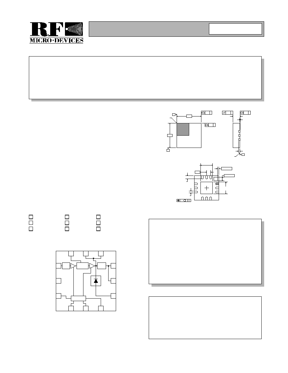
Product Description
Ordering Information
Typical Applications
Features
Functional Block Diagram
RF Micro Devices, Inc.
7628 Thorndike Road
Greensboro, NC 27409, USA
Tel (336) 664 1233
Fax (336) 664 0454
http://www.rfmd.com
Optimum Technology MatchingÆ Applied
Si BJT
GaAs MESFET
GaAs HBT
Si Bi-CMOS
SiGe HBT
Si CMOS
InGaP/HBT
GaN HEMT
SiGe Bi-CMOS
5
6
7
8
9
4
3
2
1
10
11
12
Input
Match
Output
Match
Bias
Interstage
Match
PWR SEN
BIAS1GND
RF IN
NC
VREG2
BIAS2GND
RF OUT
RF OUT
VCC2
VREG1
V
CC1
VCC2
RF5189
3V, 2.45GHz LINEAR POWER AMPLIFIER
∑ IEEE802.11B WLAN Applications
∑ 2.5GHz ISM Band Applications
∑ Wireless LAN Systems
∑ Commercial and Consumer Systems
∑ Portable Battery-Powered Equipment
∑ Spread-Spectrum and MMDS Systems
The RF5189 is a linear, medium-power, high-efficiency
amplifier IC designed specifically for battery-powered
WLAN applications such as PC cards, mini PCI, and
compact flash applications. The device is manufactured
on an advanced Gallium Arsenide Heterojunction Bipolar
Transistor (HBT) process, and has been designed for use
as the final RF amplifier in 2.5GHz WLAN and other
spread-spectrum transmitters. The device is provided in a
12-pin QFN package with a backside ground. The
RF5189 is designed to maintain linearity over a wide
range of supply voltage and power output. The RF5189 is
designed to reduce end-product BOM count by integrat-
ing all matching circuitry onto the chip.
∑ Single Power Supply 3.0V to 5.0V
∑ +30dBm Saturated Output Power
∑ 25dB Small Signal Gain
∑ High Linearity
∑ 2400MHz to 2500MHz Frequency Range
RF5189
3V, 2.45GHz Linear Power Amplifier
RF5189 PCBA
Fully Assembled Evaluation Board
0
Rev A5 040106
0.05
0.00
0.10 C
0.08 C
1.00
0.80
0.20
REF
-C-
SEATING
PLANE
Dimensions in mm.
Shaded lead is pin 1.
2 PLCS
0.10 C
3.00
-A-
2 PLCS
0.10 C
3.00
-B-
INDEX
AREA
0.50
0.50
0.30
TYP
1.45
+0.10
-0.15
0.435 SQ
1.45
+0.10
-0.15
0.18 TYP
0.10
C A B
M
0.30
0.18
Package Style: QFN, 12-Pin, 3x3
2-656
RF5189
Rev A5 040106
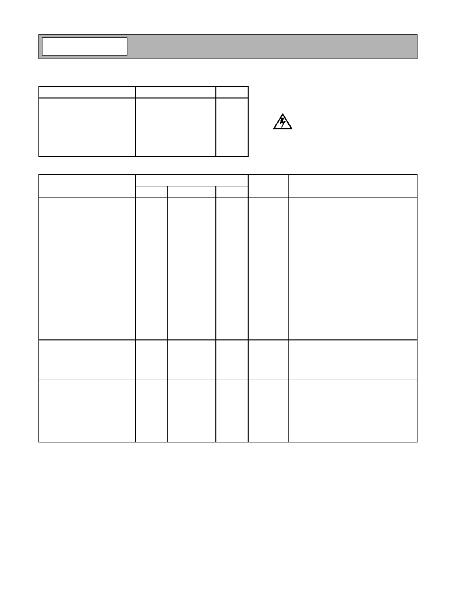
Absolute Maximum Ratings
Parameter
Rating
Unit
Supply Voltage
-0.5 to +6.0
V
DC
Power Control Voltage (V
REG
)
-0.5 to 3.5
V
DC Supply Current
600
mA
Input RF Power
+10
dBm
Operating Ambient Temperature
-40 to +85
∞C
Storage Temperature
-40 to +150
∞C
Moisture sensitivity
JEDEC Level 2
Parameter
Specification
Unit
Condition
Min.
Typ.
Max.
Overall-11b Signal
T=25∞C, V
CC
=3.0V, V
REG
=2.7V,
Freq=2450MHz
Frequency Range
2400 to 2500
MHz
Maximum Linear Output Power
With 802.11B modulation (11Mbit/s) and
meeting 802.11B spectral mask.
V
CC
=3.0V
21
22
dBm
V
CC
=5.0V
24
dBm
Linear Efficiency
24
%
Small Signal Gain
23
25
27
dB
P
IN
=-7dBm
Second Harmonic
-35
dBc
802.11B Adjacent Channel
Power
-38
-32
dBc
P
OUT
=21dBm, V
CC
=3.0V
Alternate Channel Power
-56
-52
dBc
P
OUT
=21dBm, V
CC
=3.0V
Isolation
30
dB
In "OFF" state, P
IN
=-5.0dBm
Input Return Loss
9.5
15.0
dB
50
reference
Output VSWR
2:1
1.5:1
50
reference
Power Detect Voltage
1.7
2.1
2.4
V
P
0
=21dBm
Power Down
V
REG
"ON"
2.1
2.7
3.0
V
Voltage supplied to control input;
device is "ON"
V
REG
"OFF"
0
0.5
V
Voltage supplied to control input;
device is "OFF"
Power Supply
Operating Voltage
3.0 to 5.0
V
Current Consumption
10
µ
A
V
REG
=0V
100
160
mA
No RF input, V
CC
=3.0V, and V
REG
=2.7V
220
270
mA
P
OUT
=21dBm, V
CC
=3.0V, and V
REG
=2.7V
V
REG
Current (Total)
5
10
mA
V
CC
=3.0V
10
15
mA
V
CC
=5.0V
Caution! ESD sensitive device.
RF Micro Devices believes the furnished information is correct and accurate
at the time of this printing. However, RF Micro Devices reserves the right to
make changes to its products without notice. RF Micro Devices does not
assume responsibility for the use of the described product(s).
Refer to "Handling of PSOP and PSSOP Products"
on page 16-15 for special handling information.
2-657
RF5189
Rev A5 040106
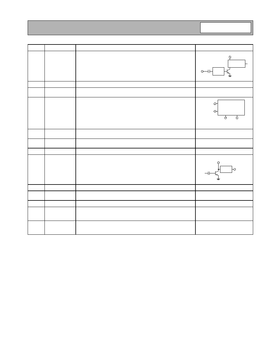
Pin
Function
Description
Interface Schematic
1
RF IN
RF input. Input is matched to 50
and DC block is provided internally.
2
NC
No connect. Recommend connecting to ground.
3
BIAS1GND
Ground for first stage bias circuit. For best performance, keep traces
physically short and connect immediately to ground plane.
See pin 4.
4
VREG1
First stage input bias. This pin requires a regulated supply to maintain
nominal bias current.
5
VREG2
Second stage input bias. This pin requires a regulated supply to main-
tain nominal bias current. Usually connected to VREG1.
See pin 4.
6
BIAS2GND
Ground for second stage bias circuit. For best performance, connect to
ground with a choke inductor.
See pin 4.
7
PWR SEN
Provides an output voltage proportional to output RF level.
8
RF OUT
RF output. Output is matched to 50
and DC block is provided inter-
nally.
9
RF OUT
Same as pin 8.
See pin 8.
10
VCC2
Second stage output bias. Supply should be connected through a
choke inductor sized appropriately to handle the output bias current.
See pin 8.
11
VCC2
Same as pin 10.
See pin 8.
12
VCC1
First stage output bias. This pin is sensitive to bypass capacitors placed
close to it. Place an RF short approximately 200mils from this pin
before any other supply connections.
See pin 1.
Pkg
Base
GND
Ground connection. The backside of the package should be connected
to the ground plane through a short path (i.e., vias under the device will
be required).
INPUT
MATCH
VCC1
INTERSTAGE
MATCH
BIAS
VREG1
VREG2
BIAS
GND1
BIAS
GND2
RF OUT
OUTPUT
MATCH
VCC2

2-658
RF5189
Rev A5 040106
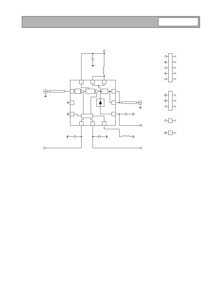
Theory of Operation
The RF5189 is a two-stage device with a nominal gain of 25dB in the 2.4GHz to 2.5GHz ISM band. The RF5189 is
designed primarily for IEEE802.11B WLAN applications where the available supply voltage and current are limited. This
amplifier will operate to (and below) the lowest expected voltage made available by a typical PCMCIA slot in a laptop PC,
and will maintain required linearity at decreased supply voltages.
The RF5189 requires only a single positive supply of 3.0V nominal (or greater) to operate to full specifications. Power
control is provided through two bias control input pins (VREG1 and VREG2), but in most applications these are tied
together and used as a single control input.
There is no external matching required on the input and output of the part, thus allowing minimal bill of material (BOM)
parts count in end applications. Both the input and the output of the device are DC-blocked.
For best results, the PA circuit layout from the evaluation board should be copied as closely as possible, particularly the
ground layout and ground vias. Other configurations may also work, but the design process is much easier and quicker if
the layout is copied from the RF5189 evaluation board. Gerber files of our designs are available on request.
The RF5189 is not a difficult part to implement, but care in circuit layout and component selection is always advisable
when designing circuits to operate at 2.5GHz. The choke inductors on VCC2 and BIAS2GND should be chosen so that
they are parallel self-resonant at the frequency of operation. In addition, the supply side of the choke inductor on VCC2
should be bypassed with a capacitor that is series self-resonant at the frequency of operation.
In practice, VCC1 and the supply side of the choke on VCC2 will be tied to the same supply. It is important to isolate
VCC1 from other RF and low-frequency bypass capacitors on this supply line. This can be accomplished using a suit-
ably-long transmission line which is RF shorted on the other end as described above. Ideally the length of this line will be
a quarter wavelength, but it only needs to be long enough so that the effects of other supply bypass capacitors on the
VCC1 line are minimized. If board space is a concern, this isolation can also be accomplished with an RF choke inductor
or ferrite bead.
The RF5189 has primarily been characterized with a voltage on VREG1 and VREG2 of 2.7V
DC
. However, the RF5189
will operate from a wide range of control voltages. If you prefer to use a control voltage that is significantly different than
2.7V
DC
, contact RFMD Sales or Applications Engineering for additional data and guidance.
2-659
RF5189
Rev A5 040106
Evaluation Board Schematic
50
µ
strip
J1
RF IN
VREG1
C3
1000 pF
VREG2
C13
1000 pF
L2
10 nH
C13
1000 pF
PDETECT
50
µ
strip
J2
RF OUT
L1
12 nH
C14
1
µ
F
VCC
P2-3
VCC1
GND
GND
P2
1
2
3
CON3
GND
GND
P1-5
VREG1
P1-3
VREG2
P1-1
PDETECT
P1
1
2
3
4
5
CON5
P3-1
VCC
P3
1
CON1
GND
P4
1
CON1
5
6
7
8
9
4
3
2
1
10
11
12
Input
Match
Output
Match
Bias
Interstage
Match

2-660
RF5189
Rev A5 040106
Evaluation Board Layout
Board Size 1.10" x 1.85"
Board Thickness 0.032", Board Material FR-4
2-661
RF5189
Rev A5 040106
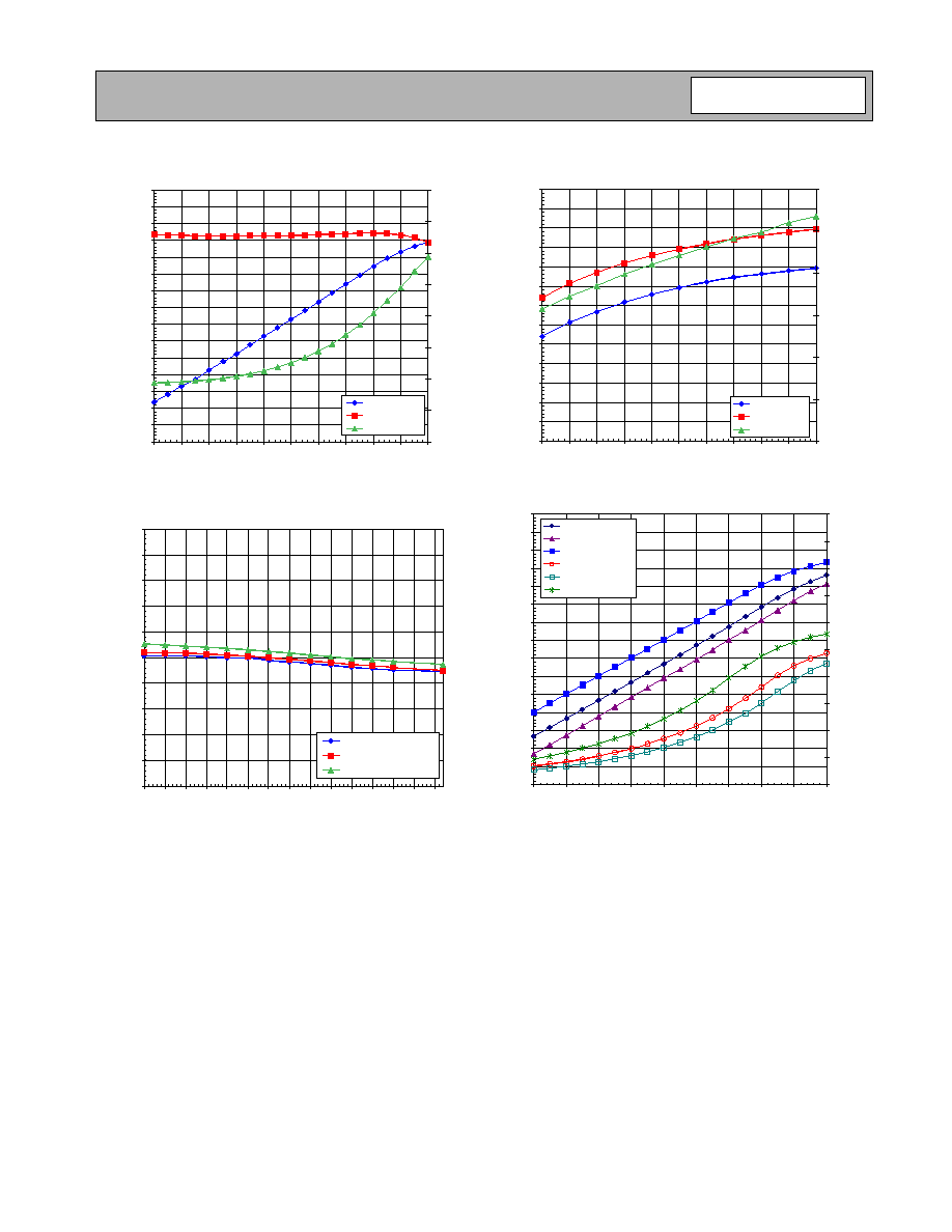
P
OUT
, Gain, I
CC
Total versus P
IN
(Typical) @ V
CC
=3.0V,
V
REG
=2.7V
0.0
2.0
4.0
6.0
8.0
10.0
12.0
14.0
16.0
18.0
20.0
22.0
24.0
26.0
28.0
30.0
-20.0 -18.0 -16.0 -14.0 -12.0 -10.0
-8.0
-6.0
-4.0
-2.0
0.0
P
IN
(dBm)
Gain (dB), P
OUT
(dBm)
0.0
50.0
100.0
150.0
200.0
250.0
300.0
350.0
400.0
I
CC
Total (mA)
Pout(dBm)
Gain(dB)
ICC_Total(mA)
P
OUT
, Gain, I
CC
Total versus V
REG
@ V
CC
=3.0V
14.0
15.0
16.0
17.0
18.0
19.0
20.0
21.0
22.0
23.0
24.0
25.0
26.0
27.0
2.0
2.1
2.2
2.3
2.4
2.5
2.6
2.7
2.8
2.9
3.0
Vreq(V)
Gain(dB), Pout(dBm)
0.0
50.0
100.0
150.0
200.0
250.0
300.0
I
CC
Total (mA)
Pout(dBm)
Gain(dB)
ICC_Total(mA)
Channel Frequency versus Gain (Typical) for V
CC
=3.0V,
3.3V, and 5.0V, V
REG1
=V
REG2
=2.7V and P
OUT
=21dBm
20.0
21.0
22.0
23.0
24.0
25.0
26.0
27.0
28.0
29.0
30.0
2.412 2.417 2.422 2.427 2.432 2.437 2.442 2.447 2.452 2.457 2.462 2.467 2.472 2.477 2.482
Frequency (GHz)
Gai
n
(
d
B)
Gain(dB)@Vcc=3.0Volts
Gain(dB)@Vcc=3.3Volts
Gain(dB)@Vcc=5.0 Volts
P
OUT
, P
DETECT
versus P
IN
(Typical) @ V
CC
=3.0, V
REG
=2.7
over Temp (-40, +25, +85)∞C
0.0
2.0
4.0
6.0
8.0
10.0
12.0
14.0
16.0
18.0
20.0
22.0
24.0
26.0
28.0
30.0
-20.0
-18.0
-16.0
-14.0
-12.0
-10.0
-8.0
-6.0
-4.0
-2.0
P
IN
(dBm)
P
OUT
(dBm)
0.0
0.5
1.0
1.5
2.0
2.5
3.0
3.5
4.0
4.5
5.0
P
DE
TE
CT
(V
)
Pout(dBm) @ + 25 C
Pout(dBm) @ +85 c
Pout(dBm) @ -40 C
PDETECT (V) @ +25 C
PDETECT (V) @ + 85 C
PDETECT (V) @ -40 C

2-662
RF5189
Rev A5 040106
I
CQ
, I
CC
_Total, P
OUT
versus V
REG
(Typical) @ V
CC
=3.0V, P
IN
=-
5dBm
0.0
20.0
40.0
60.0
80.0
100.0
120.0
140.0
160.0
180.0
200.0
220.0
240.0
260.0
280.0
300.0
1.6 1.7 1.8 1.9 2.0 2.1 2.2 2.3 2.4 2.5 2.6 2.7 2.8 2.9 3.0
V
REG
(V)
I
CQ
, I
CC
_Total (mA)
0.0
5.0
10.0
15.0
20.0
25.0
P
OUT
(dBm)
ICQ(mA)
ICC_Total(mA)
Pout(dBm)
I
REG
, P
OUT
versus V
REG
(Typical) @ V
CC
=3.0V,
P
IN
=-5.0dBm
0.0
1.0
2.0
3.0
4.0
5.0
6.0
7.0
8.0
9.0
10.0
1.6 1.7 1.8 1.9 2.0 2.1 2.2 2.3 2.4 2.5 2.6 2.7 2.8 2.9 3.0
V
REG
(V)
I
REG
_Total (mA)
0.0
2.0
4.0
6.0
8.0
10.0
12.0
14.0
16.0
18.0
20.0
22.0
24.0
26.0
28.0
30.0
P
OUT
(dBm)
Ireg(mA)
Pout(dBm)
Spectral Mask (Typical): V
CC
=3.0V, V
REG1
=V
REG2
=2.7V,
P
OUT
=18dBm, P
IN
=-7.55dBm, and I
CC
_Total=168mA
Spectral Mask (Typical): V
CC
=3.0V, V
REG1
=V
REG2
=2.7V,
P
OUT
=21dBm, P
IN
=-4.0dBm, and I
CC
_Total=210mA
2-663
RF5189
Rev A5 040106
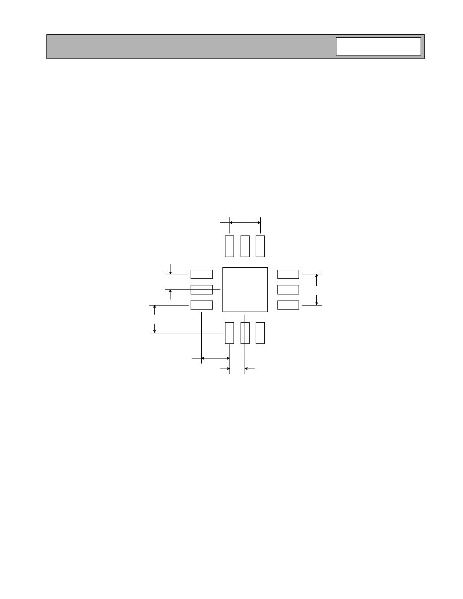
PCB Design Requirements
PCB Surface Finish
The PCB surface finish used for RFMD's qualification process is electroless nickel, immersion gold. Typical thickness is
3
µ
inch to 8
µ
inch gold over 180
µ
inch nickel.
PCB Land Pattern Recommendation
PCB land patterns are based on IPC-SM-782 standards when possible. The pad pattern shown has been developed and
tested for optimized assembly at RFMD; however, it may require some modifications to address company specific
assembly processes. The PCB land pattern has been developed to accommodate lead and package tolerances.
PCB Metal Land Pattern
B
B
B
A
A
A
B
B
B
C
A
A
A
Dimensions in mm.
Pin 1
Pin 6
Pin 9
Pin 12
0.78 Typ.
0.78 Typ.
1.00 Typ.
A = 0.69 x 0.28 (mm) Typ.
B = 0.28 x 0.69 (mm) Typ.
C = 1.45 (mm) Sq.
0.50 Typ.
1.00 Typ.
0.50 Typ.
Figure 1. PCB Metal Land Pattern (Top View)
2-664
RF5189
Rev A5 040106
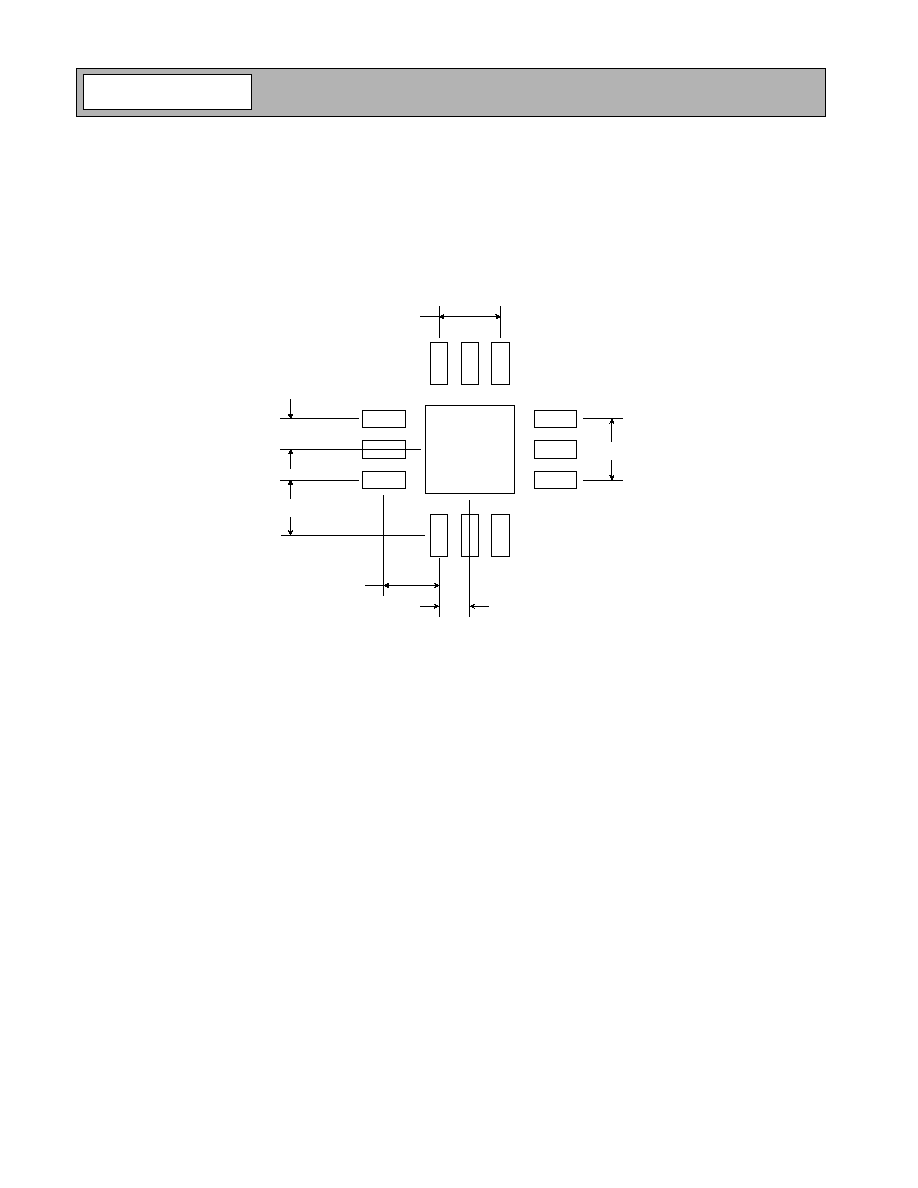
PCB Solder Mask Pattern
Liquid Photo-Imageable (LPI) solder mask is recommended. The solder mask footprint will match what is shown for the
PCB Metal Land Pattern with a 3mil expansion to accommodate solder mask registration clearance around all pads. The
center-grounding pad shall also have a solder mask clearance. Expansion of the pads to create solder mask clearance
can be provided in the master data or requested from the PCB fabrication supplier.
Thermal Pad and Via Design
The PCB Metal Land Pattern has been designed with a thermal pad that matches the exposed die paddle size on the
bottom of the device.
Thermal vias are required in the PCB layout to effectively conduct heat away from the package. The via pattern has been
designed to address thermal, power dissipation and electrical requirements of the device as well as accommodating
routing strategies.
The via pattern used for the RFMD qualification is based on thru-hole vias with 0.203mm to 0.330mm finished hole size
on a 0.5mm to 1.2mm grid pattern with 0.025mm plating on via walls. If micro vias are used in a design, it is suggested
that the quantity of vias be increased by a 4:1 ratio to achieve similar results.
B
B
B
A
A
A
B
B
B
C
A
A
A
Dimensions in mm.
Pin 1
Pin 6
Pin 9
Pin 12
0.78 Typ.
0.78 Typ.
A = 0.79 x 0.38 (mm) Typ.
B = 0.38 x 0.79 (mm) Typ.
C = 1.55 (mm) Sq.
0.50 Typ.
1.00 Typ.
1.00 Typ.
0.50 Typ.
Figure 2. PCB Solder Mask Pattern (Top View)