2-689
Product Description
Ordering Information
Typical Applications
Features
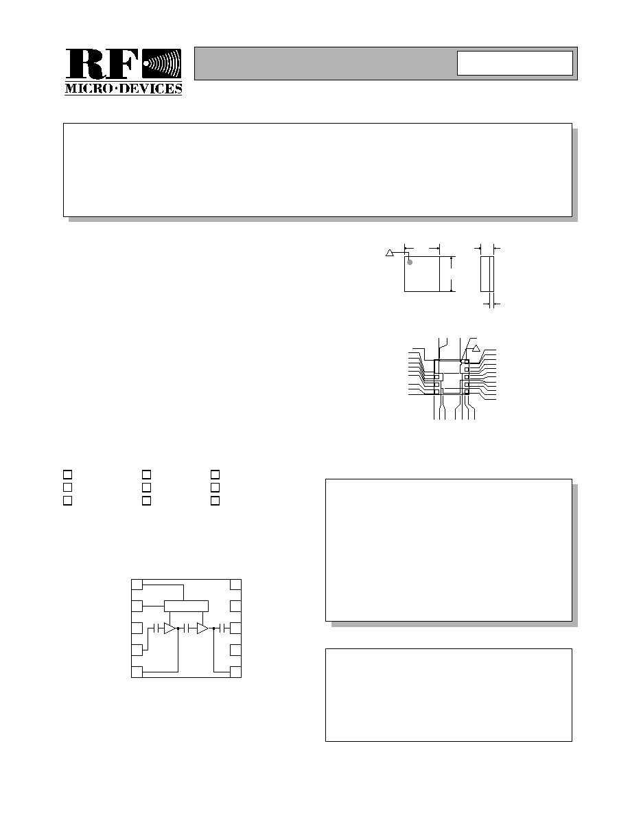
Functional Block Diagram
RF Micro Devices, Inc.
7628 Thorndike Road
Greensboro, NC 27409, USA
Tel (336) 664 1233
Fax (336) 664 0454
http://www.rfmd.com
Optimum Technology MatchingÆ Applied
Si BJT
GaAs MESFET
GaAs HBT
Si Bi-CMOS
SiGe HBT
Si CMOS
InGaP/HBT
GaN HEMT
SiGe Bi-CMOS
10
9
7
6
1
2
4
5
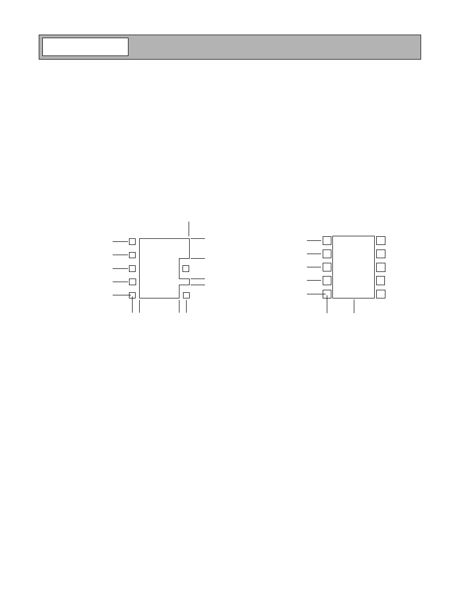
Bias
8
3
VREG
VMODE
GND
RF IN
VCC1
GND
RF OUT
VCC2
GND
GND
RF6100-1
3V 900MHZ LINEAR POWER
AMPLIFIER MODULE
∑ 3V CDMA/AMPS Cellular Handset
∑ 3V CDMA20001/X Cellular Handset
∑ Spread-Spectrum System
The RF6100-1 is a high-power, high-efficiency linear
amplifier module specifically designed for 3V handheld
systems. The device is manufactured on an advanced
third generation GaAs HBT process, and was designed
for use as the final RF amplifier in 3V IS-95/CDMA 2000
1X/AMPS handheld digital cellular equipment, spread-
spectrum systems, and other applications in the 824MHz
to 849MHz band. The RF6100-1 has a digital control line
for low power applications to lower quiescent current. The
device is self-contained with 50
input and output that is
matched to obtain optimum power, efficiency and linear-
ity. The module is a 4mmx4mm land grid array with back-
side ground. The RF6100-1 is footprint compatible with
industry standard 4mmx4mm CDMA modules, and
requires only one decoupling capacitor.
∑ Input/Output Internally Matched@50
∑ 28dBm Linear Output Power
∑ 40% Peak Linear Efficiency
∑ -50dBc ACPR @ 885kHz
∑ 29dB Linear Gain
∑ 53% AMPS Efficiency
RF6100-1
3V 900MHz Linear Power Amplifier Module
RF6100-1 PCBA Fully Assembled Evaluation Board
0
Rev A0 031219
0.450
± 0.075
1.40
1.25
4.00
± 0.10
1
4.00
± 0.10
1
3.549
3.500
3.050
2.650
2.400 TYP
2.200
1.800
1.650
1.350
0.950
0.725
0.125
R0.20 TYP
0.100 TYP
3.900 TYP
2.425
2.200
1.800
1.525
1.350
0.950
0.500 TYP
0.000
0.
775
0.
000
1.
000
TY
P
3.
000
TYP
3.
900
TY
P
3.
500
TY
P
3.
200
2.
975
0.
600 TY
P
0.
500 TY
P
Package Style: Module (4mmx4mm)

2-690
RF6100-1
Rev A0 031219
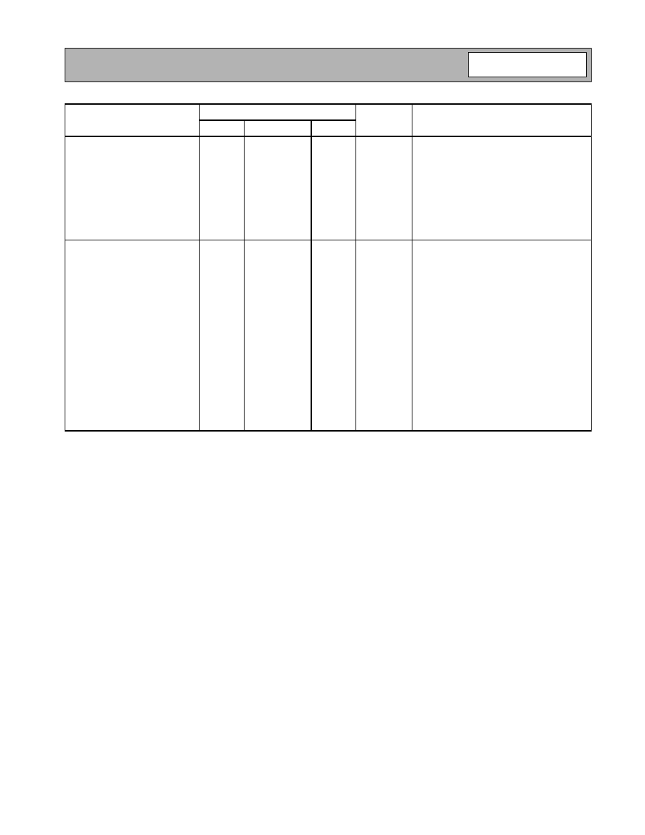
Absolute Maximum Ratings
Parameter
Rating
Unit
Supply Voltage (RF off)
+8.0
V
Supply Voltage (P
OUT
31dBm)
+5.2
V
Control Voltage (V
REG
)
+4.2
V
Input RF Power
+10
dBm
Mode Voltage (V
MODE
)
+3.5
V
Operating Temperature
-30 to +110
∞C
Storage Temperature
-40 to +150
∞C
Parameter
Specification
Unit
Condition
Min.
Typ.
Max.
High Power Mode
(V
MODE
Low)
T=25
o
C Ambient, V
CC
=3.4V, V
REG
=2.8V,
V
MODE
=0V, and P
OUT
=28dBm for all
parameters (unless otherwise specified).
Operating Frequency Range
824
849
MHz
Linear Gain
27
29
dB
Second Harmonics
-35
dBc
Third Harmonics
-40
dBc
Maximum Linear Output
28
Linear Efficiency
35
40
%
Maximum I
CC
465
530
mA
ACPR @ 885kHz
-50
-46
dBc
ACPR @ 1.98MHz
-58
-55
dBc
Input VSWR
2:1
Stability in Band
6:1
No oscillation>-70dBc
Stability out of Band
10:1
No damage
Noise Power
-133
dBm/Hz
At 45MHz offset.
Low Power Mode
(V
MODE
High)
T=25
o
C Ambient, V
CC
=3.4V, V
REG
=2.8V,
V
MODE
=2.8V, and P
OUT
=18dBm for all
parameters (unless otherwise specified).
Operating Frequency Range
824
849
MHz
Linear Gain
24
26
dB
Second Harmonics
-35
dBc
Third Harmonics
-40
dBc
Maximum Linear Output
18
Maximum I
CC
135
mA
P
OUT
=16dBm
ACPR @885kHz
-50
-46
dBc
ACPR @1.98MHz
-60
-56
dBc
Input VSWR
2:1
Output VSWR Stability
6:1
No oscillation>-70dBc
10:1
No damage
Caution! ESD sensitive device.
RF Micro Devices believes the furnished information is correct and accurate
at the time of this printing. However, RF Micro Devices reserves the right to
make changes to its products without notice. RF Micro Devices does not
assume responsibility for the use of the described product(s).
2-691
RF6100-1
Rev A0 031219
Parameter
Specification
Unit
Condition
Min.
Typ.
Max.
FM Mode
T=25
o
C Ambient, V
CC
=3.4V, V
REG
=2.8V,
V
MODE
=0V, and P
OUT
=31dBm for all
parameters (unless otherwise specified).
Operating Frequency Range
824
849
MHz
AMPS Maximum Output Power
31
dBm
AMPS Efficiency
47
53
%
AMPS Gain
24
28
AMPS Second Harmonics
-35
-30
dBc
AMPS Third Harmonics
-40
-30
dBc
Power Supply
Supply Voltage
3.2
3.4
4.2
V
High Gain Idle Current
65
100
mA
V
MODE
=low and V
REG
=2.8V
Low Gain Idle Current
55
70
mA
V
MODE
=high and V
REG
=2.8V
V
REG
Current
4.7
5.5
mA
V
MODE
=high
V
MODE
Current
250
1000
uA
RF Turn On/Off Time
6
uS
DC Turn On/Off Time
40
uS
Total Current (Power Down)
0.2
5.0
uA
V
REG
Low Voltage
0
0.5
V
V
REG
High Voltage
(Recommended)
2.75
2.8
2.95
V
V
REG
High Voltage
(Operational)
2.7
3.0
V
V
MODE
Voltage
0
0.5
V
High Gain Mode
2.0
2.8
V
Low Gain Mode
2-692
RF6100-1
Rev A0 031219
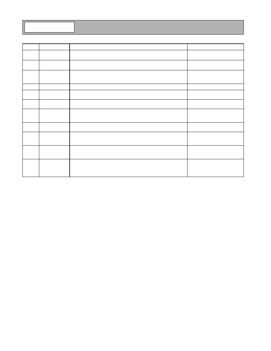
Pin
Function
Description
Interface Schematic
1
VREG
Regulated voltage supply for amplifier bias. In Power Down mode, both
V
REG
and V
MODE
need to be LOW (<0.5V).
2
VMODE
For nominal operation (High Power Mode), V
MODE
is set LOW. When
set HIGH, devices are biased lower to improve efficiency.
3
GND
Ground connection. Connect to package base ground. For best perfor-
mance, keep traces physically short and connect immediately to
ground plane.
4
RF IN
RF input internally matched to 50
. This input is internally AC-coupled.
5
VCC1
First stage collector supply. A low frequency decoupling capacitor
(e.g., 4.7
µ
F) may be required.
6
VCC2
Output stage collector supply. A low frequency decoupling capacitor
(e.g., 4.7
µ
F) is required.
7
GND
Ground connection. Connect to package base ground. For best perfor-
mance, keep traces physically short and connect immediately to
ground plane.
8
RF OUT
RF output internally matched to 50
. This output is internally
AC-coupled.
9
GND
Ground connection. Connect to package base ground. For best perfor-
mance, keep traces physically short and connect immediately to
ground plane.
10
GND
Ground connection. Connect to package base ground. For best perfor-
mance, keep traces physically short and connect immediately to
ground plane.
Pkg
Base
GND
Ground connection. The backside of the package should be soldered to
a top side ground pad which is connected to the ground plane with mul-
tiple vias. The pad should have a short thermal path to the ground
plane.
2-693
RF6100-1
Rev A0 031219
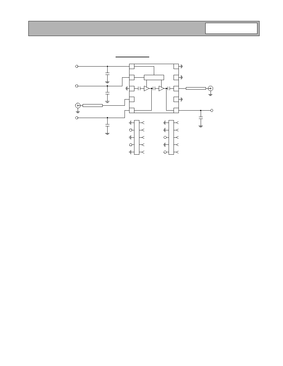
Evaluation Board Schematic
(Download Bill of Materials from www.rfmd.com.)
1
2
3
4
5
7
6
9
8
10
VREG
C3
4.7
µ
F
50
µ
strip
J2
RF OUT
50
µ
strip
J1
RF IN
VCC1
C2
4.7
µ
F
VCC2
C1
22
µ
F
C4
4.7
µ
F
VMODE
Bias
P2
1
2
3
4
5
CON5
GND
GND
GND
P2-5
VMODE
P2-3
VREG
P1
1
2
3
4
5
CON5
GND
GND
GND
P1-2
VCC1
P1-4
VCC2
2-694
RF6100-1
Rev A0 031219
PCB Design Requirements
PCB Surface Finish
The PCB surface finish used for RFMD's qualification process is electroless nickel, immersion gold. Typical thickness is
3
µ
inch to 8
µ
inch gold over 180
µ
inch nickel.
PCB Land Pattern Recommendation
PCB land patterns are based on IPC-SM-782 standards when possible. The pad pattern shown has been developed and
tested for optimized assembly at RFMD; however, it may require some modifications to address company specific
assembly processes. The PCB land pattern has been developed to accommodate lead and package tolerances.
PCB Metal Land and Solder Mask Pattern
Thermal Pad and Via Design
The PCB metal land pattern has been designed with a thermal pad that matches the exposed die paddle size on the bot-
tom of the device.
Thermal vias are required in the PCB layout to effectively conduct heat away from the package. The via pattern has been
designed to address thermal, power dissipation and electrical requirements of the device as well as accommodating
routing strategies.
The via pattern used for the RFMD qualification is based on thru-hole vias with 0.203mm to 0.330mm finished hole size
on a 0.5mm to 1.2mm grid pattern with 0.025mm plating on via walls. If micro vias are used in a design, it is suggested
that the quantity of vias be increased by a 4:1 ratio to achieve similar results.
Pin 1
Metal Land Pattern
0.00
0.00
0.45 (m
m)
2.95 (
m
m)
Ty
p.
3.40 (
m
m)
Ty
p.
0.85 (mm) Typ.
1.70 (mm) Typ.
2.55 (mm)
3.40 (mm)
0.65 (mm)
1.05 (mm)
2.35 (mm)
3.60 (mm)
3.6
0
(mm)
Typ.
A = 0.40 (mm) Sq. Typ.
A
A
A
A
A
A
A
3.40 (mm) Typ.
A = 0.55 (mm) Sq. Typ.
B = 2.65 x 3.95 (mm)
1
.
70 (mm)
Pin 1
Solder Mask Pattern
0.0
0
0.00
0.85 (mm) Typ.
1.70 (mm) Typ.
2.55 (mm) Typ.
A
A
A
A
A
A
A
A
A
A
B
Figure 1. PCB Metal Land and Solder Mask Pattern (Top View)