 | –≠–ª–µ–∫—Ç—Ä–æ–Ω–Ω—ã–π –∫–æ–º–ø–æ–Ω–µ–Ω—Ç: TA0031 | –°–∫–∞—á–∞—Ç—å:  PDF PDF  ZIP ZIP |
13-157
13
T
E
CH
NIC
A
L
NO
T
E
S
AN
D A
R
T
I
C
L
E
S
Copyright 1997-2000 RF Micro Devices, Inc.
�
Narrow band receivers utilizing crystal referenced
phase locked loops (PLL) allow for cost effective trans-
mitters, receivers, and transceivers to be constructed
with receiver sensitivities in the -97dBm range for fre-
quency shift keying (FSK) with bit error rates (BER) of
10
-4
(-94dBm for amplitude shift keying (ASK)). This is
possible because of the availability of low cost crystals,
which provide the required frequency accuracy to use
narrow band IF filters. These 10.7MHz ceramic filters
come in bandwidths of 110 kHz to 360 kHz and are
available (in volume) for less than 40 cents each. SAW
solutions are accompanied by frequency tolerances
and drift on the order of 200kHz as compared to
50kHz for a crystal available (in volume) for less than
50 cents. In applications such as the European
868MHz to 870 MHz ISM band, the majority of the allo-
cated bandwidth must be used to accommodate the
SAW center frequency drift (Subband A 600kHz, Sub-
band B 500kHz), leaving little room for modulation
sidebands. Noise bandwidth for the SAW approaches
is typically 800 kHz. Sensitivities of the SAW solutions
are in the -80dBm range due to the increased noise
bandwidth as well as receiver noise figure. The PLL
approach offers approximately 7dB of sensitivity
improvement due to decreased noise bandwidth and
7 dB due to receiver noise figure.
The RF2510 is a Frequency Synthesizer Integrated
Circuit designed for use in ISM Band Transmitter Prod-
ucts, including the European 433.05MHz to
434.79MHz and 868MHz to 870 MHz Bands, as well
as the United States 902MHz to 928MHz Band. In
general, the RF2510 can be used over the 300MHz to
1000 MHz range. The RF2510 integrates PLL compo-
nents such as a voltage controlled oscillator (VCO),
prescaler, crystal oscillator (RefOsc), phase detector,
charge pump, and power down circuitry. A modulation
pin is also provided for FM or FSK applications using
on-chip diodes. The RF2510 is available in 16 pin plas-
tic surface mount packaging (SSOP-16). With a 9mA
typical current draw at 3Volts and 10.5mA at 3.6Volts,
the RF2510 is well suited for battery powered applica-
tions.
This article discusses the design and measurement of
a frequency synthesizer to be used in ISM band appli-
cations. The formulas used for calculation of key
parameters are presented and measurement results
are shown. Particular emphasis is given to the trade-
offs between loop bandwidth and phase noise, two key
parameters of any frequency synthesizer design. All
measurements were performed with a spectrum ana-
lyzer, and the data presented is typical of a standard
product evaluation board routinely assembled for cus-
tomer sampling.
�
�
Figure 1 shows a functional block diagram for the
RF2510. The crystal oscillator topology is a modified
Colpitts type which requires two external capacitors as
well as the crystal to be connected to Pins 1 and 2 as
shown. In addition, an external reference oscillator can
be injected at Pin 1 when one is already available,
eliminating the need for the Colpitts circuitry discussed
above.
Pin 4 is the output of the transmitter. An output attenu-
ator can be used to decrease sensitivity to output
VSWR and a harmonic filter is used to meet the ISM
band specifications.
The power down pin (Pin 7) is used to disable the on-
board voltage reference. It is active low so that a DC
voltage less than 1 Volt powers down the RF2510. Cur-
rent consumption in power down mode is less than
1 microamp.
The division ratio N of the prescaler is controlled by the
logic levels at Pins 9 and 10. Depending on the combi-
nation shown in Figure 1, divisors of 64, 65, 128, or
129 can be achieved.
Pins 11 through 13 are associated with the VCO.
MODIN (Pin 12) is connected to the smaller tuning
diodes used to FM or FSK the VCO. An external varac-
tor circuit is connected between Pins 11 and 13 for
locking the VCO to the required center frequency as
well as flexibility in tuning range and/or sensitivity. The
VCO inductors are connected to Pins 11 and 13 and
they serve to set the center frequency as well as pro-
vide bias current to the oscillator.
The outputs of the on-chip charge pumps are con-
nected to the loop filter pin (Pin 14). A common loop fil-
ter for low cost synthesizers is a one port three
element passive filter, however higher performance two
port passive or active filter topologies could also be
used. The voltage on the loop filter pin tunes the varac-
TA0031
TA0031
RF2510: Frequency Synthesis Using the RF2510

13-158
TA0031
13
T
E
CH
NIC
A
L
NO
T
E
S
AN
D A
R
T
I
C
L
E
S
Copyright 1997-2000 RF Micro Devices, Inc.
tor of the VCO.
Figure 1. RF2510 Functional Block Diagram
�
Figure 2 shows a block diagram of a generalized PLL
showing the feedforward function G(s) and feedback
function H(s). The transfer functions of the PLL can be
expressed in terms of these functions as shown.
Figure 2. General PLL Transfer Functions
Figure 3 shows the design of a third order type 2
charge pump based PLL. The loop filter for this design
is a one port, three element passive filter. All the
design equations needed for the loop design are
shown in Figure 3. Phase margins of 45degrees to
60degrees are typically used to guarantee loop stabil-
ity.
Figure 3. Charge Pump PLL Design Equations
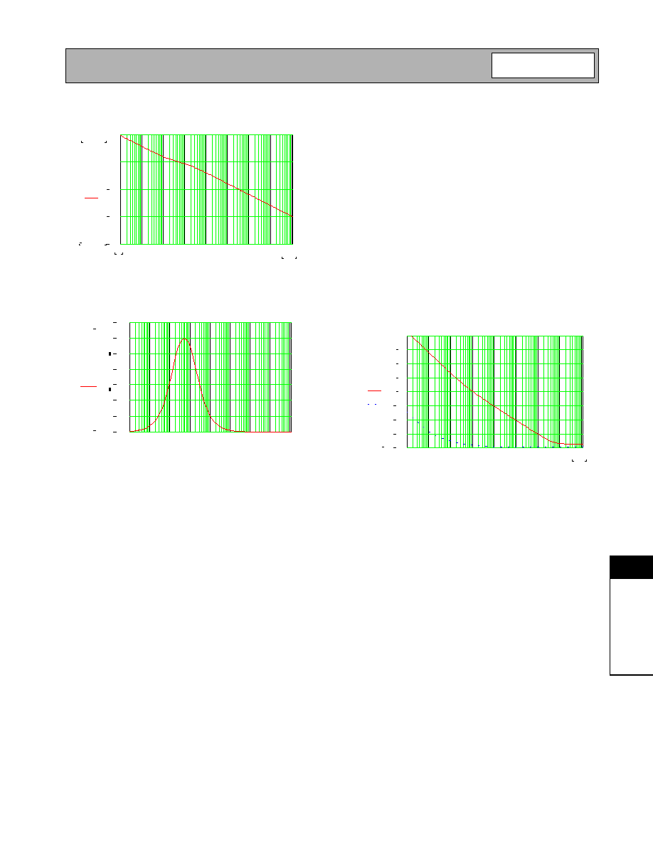
Figures 4 and 5 show the open loop gain and phase for
a sample PLL. As can be seen, the loop BW is 5kHz
and the phase margin is 60degrees. The loop BW is
defined as the frequency where the open loop transfer
function reaches unity gain and the phase margin is
the difference between the phase at unity gain and
180degrees.
5
6
8
PHASE
DETECTOR
128/129
or 64/65
9
1
2
3
4
7
REFB
REFE
PWR_DWN
VCC
LPFLT
NC
GND
MODIN
LON
DIV64ON
MODCTL
LO
10
11
12
13
14
15
16
CHARGE
PUMPS
Vcc
Output
Vcc
1/64 1/65 1/128 1/129
H H L L
H L H L
m(t)
/N
GND
NC
VREFP
+ _
�
�
�
[
�
�
�
�
! ! " "
�
�
#
$
%#
% $
" & � ' ( � � ! ) ) " *
% + '
% + ' !
! " "
, ( -. -
& �
, / # �0
�
- 1
$ �
�
( (
2 /-
� � (
& 2 / (� �
�
� �
�
!
�
"
# $ %
& � '
() '
(
* !
#
+ &
*
& )
&
&
& )
+
, +
- ,
. &
&
/
13-159
TA0031
13
T
E
CH
NIC
A
L
NO
T
E
S
AN
D A
R
T
I
C
L
E
S
Copyright 1997-2000 RF Micro Devices, Inc.
Figure 4. Open Loop Gain
Figure 5. Open Loop Phase
� ��
Oscillator phase noise is usually characterized with
Leeson's model (as shown in Equation1). The oscilla-
tor active device has a 1/f phase noise corner fre-
quency. This is approximately 5kHz for Silicon NPN
and 5 MHz for GaAs MESFET at 900 MHz. When
placed in a feedback loop to form an oscillator this 1/f
phase noise is scaled by the circuit group delay
= 2Q
L
/
0
into frequency noise. Since phase is the
integral of frequency, the resulting frequency noise
spectral density is divided by the offset frequency to
convert or integrate to phase noise. The term in
Equation1 is squared because L(f) is a noise power
ratio. The noise floor of the oscillator is determined by
the amplifier compressed gain, noise figure, output
power, and thermal noise (kT). When the 1/f model
terms drop below the noise floor, Equation 1 is approx-
imately equal to the noise floor.
Equation 1. Leeson's Formula for Phase Noise
Figure 6 shows phase noise calculated for a reference
oscillator at 7.15MHz and a VCO at 915.2MHz. The
floors of the two oscillators are approximately the
same, while the very large Q of the crystal oscillator
results in much lower 1/f noise.
Figure 6. Oscillator Phase Noise
Figure 7 shows several PLL noise transfer functions of
interest to estimate PLL phase noise. The reference
oscillator and divider noise will be multiplied by the
closed loop PLL transfer function. Inside the loop band-
width, this is equivalent to adding 20logN to the phase
noise of both the reference oscillator and the divider.
Outside the loop bandwidth, contributions by the refer-
ence oscillator and divider to the phase noise charac-
teristic are attenuated due to the lowpass characteristic
of the closed loop transfer function. The VCO noise is
multiplied by a highpass function which is inversely
proportional to the open loop gain. It is unity for offsets
much greater than the loop bandwidth and rolls for off-
sets less than the loop bandwidth.
The third noise transfer function is that due to noise on
the VCO tune line coming from the phase detector.
This noise voltage will modulate the VCO and impact
the overall phase noise. Since it is injected at a point
between previously defined transfer functions, it can be
scaled by the phase detector gain Kpd and then multi-
plied by the closed loop gain to get its contribution to
�
.
�
�
�
�
! !
"
#$ "
! ! %
&'
! ! %
() *+, %# )-#
.
$ $
/ %#
�
.
13-160
TA0031
13
T
E
CH
NIC
A
L
NO
T
E
S
AN
D A
R
T
I
C
L
E
S
Copyright 1997-2000 RF Micro Devices, Inc.
the output. This equation is shown in Figure 7 and
Figure 8 shows the noise characteristic of the VCO, the
Reference Oscillator + 20logN, the Divider noise
+20logN, and a noise voltage on the tune line multi-
plied by the phase detector noise gain. Note that this
noise voltage could arise from a number of sources,
including varactors in the VCO, loop filter components,
or from the phase detector/charge pump circuitry.
Figure 7. PLL Noise Transfer Functions
For an optimal phase noise design, loop bandwidth is
normally chosen as the intersection of the VCO curve
and the multiplied reference or divider curve, whichever
occurs at the lower frequency. In the case of Figure 8,
this would be approximately 20kHz. In other instances
lock time may be of prime concern and bandwidth is
set to approximately 4 divided by the locktime. Also,
when direct modulation of the VCO is required, the
loop BW must be set lower than the modulation fre-
quency in order to keep the PLL from canceling the
modulation. Manchester encoding can be used to keep
long strings of 1's or 0's from being cancelled by the
PLL, due to their low apparent frequency despite the
higher data rate.
Figure 8. PLL Phase Noise Contributors for
BW= 5kHz
Figure 9 shows the results of multiplying the noise
sources by their respective transfer functions and Fig-
ure 10a shows the composite noise curve generated
by the RMS sum of the four noise curves. Note the
peaking in the noise characteristic due to the loop
bandwidth being set below the crossover frequency
shown in Figure 8. Figure 10b shows the result if the
loop BW is set to 100kHz. In this case, the result is a
pedestal in the noise response caused by the divider
noise.
Figure 9. PLL Noise Contributors for BS=5 kHz
(modified by PLL)
'( 0 '(
'(
0 '(
[
'(- '(
'(1
0 '(
'(-0 '( '(
'(
"
'(
'( 0 '(2&) 0 '( '(1
�
" 0 '( '( �
�
�
�
+
+
+
+
�
� � �
�
�
"
'($ % # " * +
" 2!3 '(1 $ % #
�
"
'( # &2& ) " 1 #
�
+
+
% #
�
.
.
.
�
.
13-161
TA0031
13
T
E
CH
NIC
A
L
NO
T
E
S
AN
D A
R
T
I
C
L
E
S
Copyright 1997-2000 RF Micro Devices, Inc.
Figure 10a. Overall PLL Phase Noise (BW= 5kHz)
Figure 10b. Overall PLL Phase Noise (BW = 100kHz)
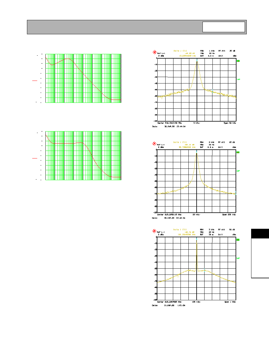
Figure 11 shows measured PLL phase noise for band-
widths of 5 kHz and 100 kHz. Figure 11a indicates a
phase noise at 10 kHz offsets of -49-31=-80 dBc/Hz,
taking into account the 1kHz resolution BW. Figure
11b indicates a phase noise of approximately
-65-35 =-100 dBc/ Hz at 100kHz offsets. Figure 11c
shows the phase noise for 100kHzBW, which has the
same noise pedestal shown in Figure 10b. Figure 12
shows measured phase noise data at 10 kHz and
100kHz as loop BW is varied. From this plot the opti-
mum loop BW for phase noise can be seen to be in the
10 to 20kHz range. Due to modulation at 9600 baud,
the RF2510 evaluation boards are typically configured
for 5kHz loop BW.
Figure 11a. Measured Phase Noise (BW= 5kHz)
Figure 11b. Measured Phase Noise (BW =5kHz)
Figure 11c. Measured Phase Noise (BW= 100 kHz)
�
�

13-162
TA0031
13
T
E
CH
NIC
A
L
NO
T
E
S
AN
D A
R
T
I
C
L
E
S
Copyright 1997-2000 RF Micro Devices, Inc.
Figure 12. Measured Phase Noise as a Function of
Loop BW
Once the phase noise characteristic is obtained, infor-
mation such as Jitter, RMS Phase Deviation, and RMS
Frequency Deviation or Residual FM can be deter-
mined. Jitter is obtained by integrating the phase noise
over a specified bandwidth. Figure 13 shows results of
this integration for different bandwidths using 10Hz as
the lower limit. For upper limits of 100Hz and above,
the Jitter is approximately 2x10
-5
rad
2
. RMS Phase
Deviation is the square root of the Jitter. Figure 14
shows the RMS Phase Deviation in degrees. For upper
limits of 100 Hz and above, the RMS Phase Deviation
is approximately .25degrees. RMS Frequency Devia-
tion or Residual FM is obtained by multiplying the
phase noise by a frequency term and then integrating
over a specified bandwidth. Figure 15 shows the RMS
Frequency Deviation or Residual FM which is approxi-
mately 1Hz for an upper limit of integration of 3MHz. In
practice, this upper limit is determined by filters which
limit the noise bandwidth. Figure 16 shows the equa-
tions for calculating the above parameters from phase
noise plots and Table 1 shows some data sheet param-
eters for the RF2510.
.Figure 13. Jitter in rad
2
for BW= 10 Hz-fh Hz
Figure 14. RMS Phase Deviation in deg for BW=
10 Hz-fh Hz
Figure 15. RMS Frequency Deviation or Residual
FM in Hz for BW = 10Hz-fh Hz
Figure 16. Parameters Calculated from L(f)
RF2510 Phase Noise vs. PLL BW
-105
-100
-95
-90
-85
-80
-75
10
100
Offset, kHz
dBc/Hz
1k
5k
10k
20k
50k
100k
�
.
�
.
.
!
" #
$
.
%
!

13-163
TA0031
13
T
E
CH
NIC
A
L
NO
T
E
S
AN
D A
R
T
I
C
L
E
S
Copyright 1997-2000 RF Micro Devices, Inc.
Table 1. RF2510 Data Sheet Parameters
�
The RF2510 is a Frequency Synthesizer Integrated
Circuit designed for ISM Band transmitter applications.
Its features have been discussed, and trade-offs
between PLL parameters and phase noise have been
presented. The RF2510 integrates PLL components
such as a VCO, prescaler, RefOsc, phase detector,
charge pump, and power down circuitry. The IC is
available in industry standard SSOP-16 packaging and
can be used to construct low cost transmitters.
4. Leeson, D.B. "A Simple Model of Feedback Oscilla-
tor Noise Spectrum", Proceedings of the IEEE,
Vol.54, Feb.1966, pp.329-330.
5. Scherer, Dieter. "Today's Lesson - Learn About Low
Noise Design", Microwaves, May1979, pp.72-77.
6. Hock, Terrence. "Synthesizer Design With Detailed
Noise Analysis", RF Design, July1993, pp.37-48.
Parameter:
Specification
Units
Min
Typ
Max
General Characteristics
Frequency Range
300
433, 868, 915
1000
MHz
Modulation Options
FM/FSK
Transmitter RF Characteristics
Output Power (50 ohm load)
-5.5
dBm
Modulation Rate
2
MHz
Max. FM Deviation
200
kHz
PLL/Prescaler Characteristics
Prescaler Divide Ratio
64/65/128/129
PLL Lock Time
4/Loop BW
ms
PLL Phase Noise (100kHz offset, 5kHz Loop BW)
-98
dBc/Hz
Crystal Startup
2
4
ms
Max. Crystal Rs
50
Charge Pump Output Current
+/-40
uA
Harmonics (with three element lowpass filter on board)
-50
-41.25
dBm
Spurious
-62
-49.2
dBm
VCO Gain, K
VCO
(dependent upon external components)
70
MHz/V
Power Supply
Operating Voltage
2.4
3.6
5.0
V
Tx Mode Current Consumption (3.6V)
7.5
10.5
13.5
mA
Sleep Mode Current Consumption
1
uA
Temperature Range
-40
+85
∞C
Package
16 pin QSOP, plastic
Note 1: The PLL Lock time is externally programmable through appropriate selection of an external resistor and capacitor (see application circuit)

13-164
TA0031
13
T
E
CH
NIC
A
L
NO
T
E
S
AN
D A
R
T
I
C
L
E
S
Copyright 1997-2000 RF Micro Devices, Inc.