 | –≠–ª–µ–∫—Ç—Ä–æ–Ω–Ω—ã–π –∫–æ–º–ø–æ–Ω–µ–Ω—Ç: RT9166 | –°–∫–∞—á–∞—Ç—å:  PDF PDF  ZIP ZIP |

Preliminary
RT9166/A
DS9166A-03 July 2003
www.richtek.com
1
300/500mA, Ultra-Fast Transient Response LDO Regulator
General Description
The RT9166/A series are CMOS low dropout
regulators optimized for ultra-fast transient response.
The devices are capable of supplying 300mA or 500mA
of output current with a dropout voltage of 230mV or
430mV respectively.
The RT9166/A's performance is optimized for
CD/DVD-ROM, CD/RW or wireless communication
supply applications. The RT9166/A regulators are
stable with output capacitors as low as 1
µF. The other
features include ultra low dropout voltage, high output
accuracy, current limiting protection, and high ripple
rejection ratio.
The devices are available in fixed output voltages
range of 1.2V to 4.5V with 0.1V per step. The
RT9166/A regulators are available in 3-lead SOT-23,
SOT-89, SOT-223 and TO-92 packages.
Ordering Information
RT9166/A-
Features
Low Quiescent Current (Typically 220
µA)
Guaranteed 300/500mA Output Current
Low Dropout Voltage: 230/430mV at 300/500mA
Wide Operating Voltage Ranges: 3V~5.5V
Ultra-Fast Transient Response
Tight Load and Line Regulation
Current Limiting Protection
Thermal Shutdown Protection
Only low-ESR Ceramic Capacitor Required for
Stability
Custom Voltage Available
Applications
CD/DVD-ROM, CD/RW
Wireless LAN Card/Keyboard/Mouse
Battery-Powered Equipment
XDSL Router
PCMCIA Card
Marking Information
For marking information, contact our sales
representative directly or through a RichTek
distributor located in your area, otherwise visit our
website for detail.
Operating Temperature Range
C: Commercial Standard
Package Type
VL : SOT-23
X : SOT-89
XL : SOT-89 L type
G : SOT-223
GL : SOT-223 L type
Z : TO-92
Output Voltage
12 : 1.2V
13 : 1.3V
:
45 : 4.5V
500mA Output Current
300mA Output Current

RT9166/A
Preliminary
www.richtek.com
DS9166A-03 July 2003
2
Pin Configurations
Part Number
Pin Configurations
RT9166-
CVL
(Plastic SOT-23)
TOP VIEW
1. GND
2. VOUT
3. VIN
RT9166/A-
CG
(Plastic SOT-223)
TOP VIEW
1. VOUT
2. GND (TAB)
3. VIN
RT9166/A-
CGL
(Plastic SOT-223)
TOP VIEW
1. GND
2. VIN (TAB)
3. VOUT
RT9166/A-
CX
(Plastic SOT-89)
TOP VIEW
1. VOUT
2. GND (TAB)
3. VIN
RT9166/A-
CXL
(Plastic SOT-89)
TOP VIEW
1. GND
2. VIN (TAB)
3. VOUT
RT9166/A-
CZ
(Plastic TO-92)
TOP VIEW
1. VIN
2. GND
3. VOUT
Typical Application Circuit
Note: To prevent oscillation, a 1
µF minimum X7R
or X5R ceramic is strongly recommended if
ceramics are used as input/output capacitors.
When using the Y5V ceramic, the minimum value
of the input/output capacitance that can be used
for stable over full operating temperature range is
3.3
µF. (see Application Information Section for
further details)
Pin Description
Pin Name
Pin Function
VIN Supply
Input
VOUT Regulator
Output
GND Common
Ground
Function Block Diagram
VOUT
VIN
GND
Error Amp
1.2V
Reference
+
_
Current
Limiting
Sensor
Thermal
Shutdown
VIN
VOUT
GND
V
OUT
V
IN
1
µF
C
OUT
RT9166/A
1
µF
C
IN
+
_
+
_
VIN
VOUT
GND
V
OUT
V
IN
1
µF
C
OUT
1
µF
C
OUT
RT9166/A
1
µF
C
IN
1
µF
C
IN
+
_
+
_
+
_
+
_
1
3
2
1
2
3
1
2
3
1
2
3
1
2
3
1 2 3
Preliminary
RT9166/A
DS9166A-03 July 2003
www.richtek.com
3
Absolute Maximum Ratings
(Note 1)
Supply Input Voltage
6.5V
Power Dissipation, P
D
@ T
A
= 25
∞C
SOT-23
0.25W
SOT-223
2W
SOT-89
0.5W
TO-92
0.6W
Package Thermal Resistance
SOT-23,
JA
250
∞C/W
SOT-223,
JC
15
∞C/W
SOT-223,
JA
60
∞C/W
SOT-89,
JC
100
∞C/W
SOT-89,
JA
180
∞C/W
TO-92,
JA
160
∞C/W
Lead Temperature (Soldering, 10 sec.)
260
∞C
Junction Temperature
150
∞C
Storage Temperature Range
-65∞C to 150∞C
ESD Susceptibility (Note 2)
HBM 2kV
MM 200V
Recommended Operating Conditions
(Note 3)
Supply Input Voltage
2.8V to 5.5V
Junction Temperature Range
-40∞C to 125∞C
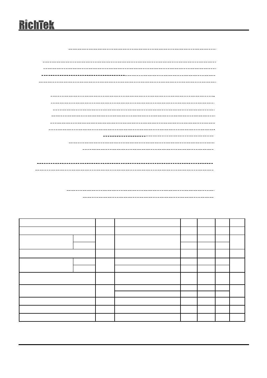
Electrical Characteristics
(V
IN
= V
OUT
+ 1V or V
IN
= 2.8V whichever is greater, C
IN
= 1
µF, C
OUT
= 1
µF, T
A
= 25
∞C, unless otherwise specified)
Parameter Symbol
Test
Conditions
Min
Typ
Max Units
Output Voltage Accuracy
V
OUT
I
OUT
= 1mA
-1
-- +3 %
RT9166 300
--
--
Current Limit
RT9166A
I
LIM
R
LOAD
= 1
500 -- --
mA
Quiescent Current (Note 6)
I
Q
I
OUT
= 0mA
-- 220
300
µA
RT9166 I
OUT
= 300mA
--
230
--
Dropout Voltage (Note 4)
RT9166A
V
DROP
I
OUT
= 500mA
--
430
--
mV
Line Regulation
V
LINE
V
IN
= (V
OUT
+ 0.3V) to 5.5V,
I
OUT
= 1mA
-- 0.2 --
%/V
1mA
< I
OUT
< 300mA
-- 15 35
Load Regulation (Note 5)
V
LOAD
1mA
< I
OUT
< 500mA
-- 25 50
mV
Power Supply Rejection Rate
PSRR f = 1kHz, C
OUT
= 1
µF --
-55
-- dB
Thermal Shutdown Temperature
T
SD
-- 170 --
∞C
Thermal Shutdown Hysteresis
T
SD
--
40
--
∞C

RT9166/A
Preliminary
www.richtek.com
DS9166A-03 July 2003
4
Note 1. Stresses beyond those listed under "Absolute Maximum Ratings" may cause permanent damage to the device.
These are stress ratings only, and functional operation of the device at these or any other conditions beyond those
indicated in the operational sections of the specifications is not implied. Exposure to absolute maximum rating
conditions for extended periods may affect device reliability.
Note 2. Devices are ESD sensitive. Handling precaution recommended. The human body model is a 100pF capacitor
discharged through a 1.5K
resistor into each pin.
Note 3. The device is not guaranteed to function outside its operating conditions.
Note 4. Dropout voltage is defined as the input to output differential at which the output voltage drops
1
% below its nominal
value measured at 1V differential. Dropout voltage does not apply to some lower voltage versions since the dropout
voltage limited by input voltage range limitations.
Note 5. Regulation is measured at constant junction temperature by using a 20mS current pulse. Devices are tested for load
regulation in the load range from 1mA to 300mA and 500mA respectively.
Note 6. Quiescent, or ground current, is the difference between input and output currents. It is defined by I
Q
= I
IN
≠ I
OUT
under no load condition (I
OUT
= 0mA). The total current drawn from the supply is the sum of the load current plus the
ground pin current.

Preliminary
RT9166/A
DS9166A-03 July 2003
www.richtek.com
5
Typical Operating Characteristics
Dropout Voltage vs. Output Current
0
100
200
300
400
500
600
0
100
200
300
400
500
Dr
op
out
Vol
t
a
ge
(
m
V
)
T
J
= +25∞C
Output Current (mA)
T
J
= -40∞C
T
J
= +125∞C
V
IN
= 5V
C
IN
= 1
µF
C
OUT
= 1
µF
Power Supply Rejection Ratio
-60
-50
-40
-30
-20
-10
0
10
100
1000
10000
100000
1000000
Frequency (Hz)
PSR
R (
d
B
)
10 100 1k 10k 100k 1M
100mA
1mA
V
IN
= 5V
C
IN
= 1
µF
C
OUT
= 1
µF
Output Noise
Time: 1mS/Div
V
IN
= 5V I
LOAD
= 100mA
C
IN
= 1
µF C
OUT
= 1
µF
400
200
0
-200
-400
Output Noise Signal (
µ
V)
f = 10Hz to 100kHz
Current Limit vs. Input voltage
700
750
800
850
900
3
3.5
4
4.5
5
5.5
C
u
rre
n
t
L
i
m
i
t (m
A
)
RT9166-33CVL
V
IN
= 5V
C
IN
= 1
µF
C
OUT
= 1
µF
R
L
= 0.5
Current Limit vs. Input voltage
700
750
800
850
900
3
3.5
4
4.5
5
5.5
Input voltage (V)
C
u
rre
n
t
L
i
m
i
t (
m
A
)
V
IN
= 5V
C
IN
= 1
µF
C
OUT
= 1
µF
R
L
= 0.5
RT9166-33CX
Range of Stable ESR
0.01
0.1
1
10
100
0
100
200
300
400
500
Output Current (mA)
O
u
t
p
ut
C
a
pa
ci
t
o
r
ES
R
C
OUT
= 10
µF
Unstable Region
Stable Region
C
OUT
= 1
µF
(
)