RT9167/A
DS9167/A-14 June 2003
www.richtek.com
1
Low-Noise, Fixed Output Voltage,
200mA/500mA LDO Regulator
General Description
The RT9167/A is a 200mA/500mA low dropout and
low noise micropower regulator suitable for portable
applications. The output voltages range from 1.5V to
5.0V in 100mV increments and 2% accuracy. The
RT9167/A is designed for use with very low ESR
capacitors. The output remains stable even with 1
µF
ceramic output capacitor.
The RT9167/A uses and internal PMOS as the pass
device, which does not cause extra GND current in
heavy load and dropout conditions. The shutdown
mode of nearly zero operation current makes the IC
suitable for battery-power devices. Other features
include a reference bypass pin to improve low noise
performance, current limiting, and over temperature
protection.
Ordering Information
RT9167/A-
Marking Information
For marking information, contact our sales
representative directly or through a RichTek
distributor located in your area, otherwise visit our
website for detail.
Features
Stable with Low-ESR Output Capacitor
Low Dropout Voltage (220mV and 200mA)
Low Operation Current - 80
µA Typical
Shutdown Function
Low Noise Output
Low Temperature Coefficient
Current and Thermal Limiting
Custom Voltage Available
SOT-25 and SOP-8 Packages
Applications
Cellular Telephones
Laptop, Notebook, and Palmtop Computers
Battery-powered Equipment
Hand-held Equipment
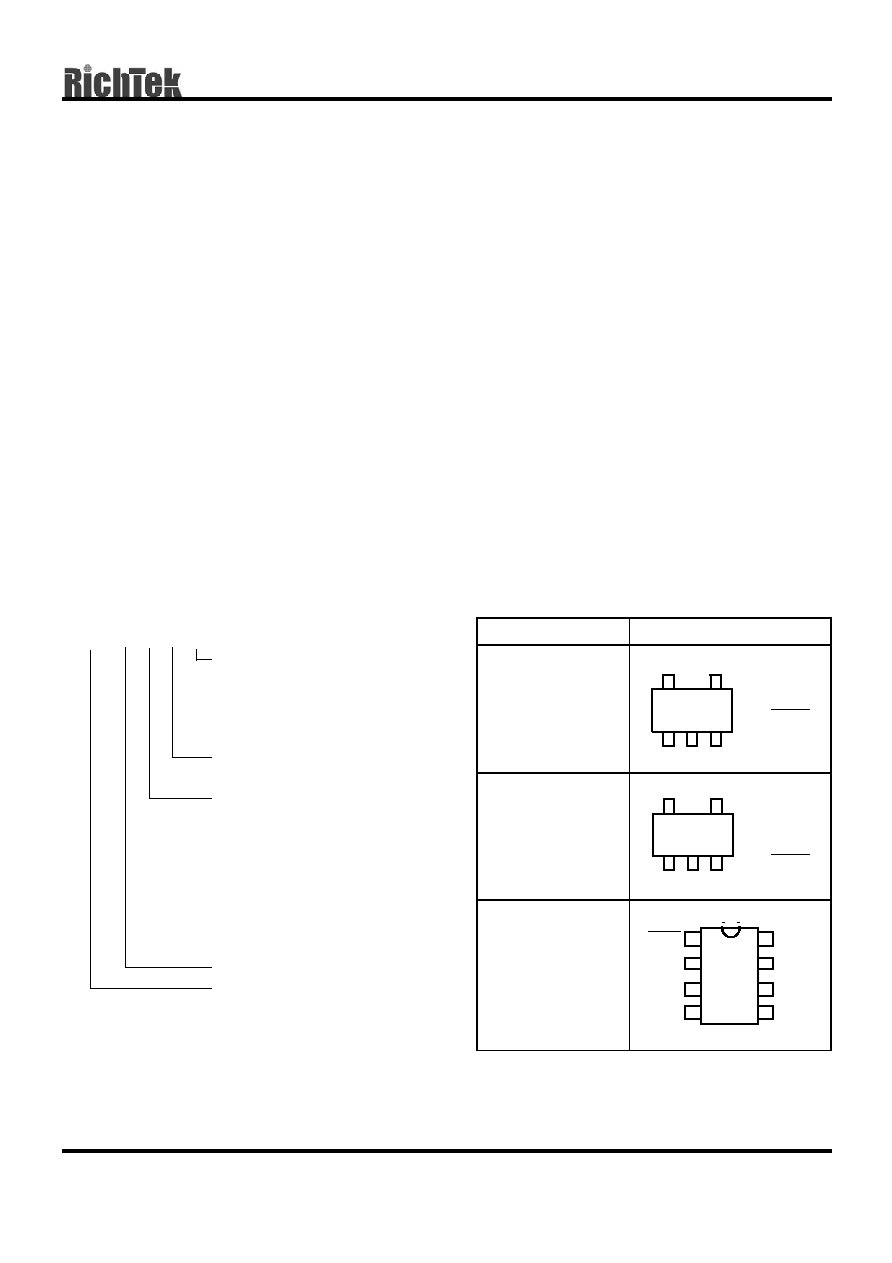
Pin Configurations
Part Number
Pin Configurations
RT9167/A-
CB
(Plastic SOT-25)
TOP VIEW
1. IN
2. GND
3. SHDN
4. BP
5. OUT
RT9167/A-
CBR
(Plastic SOT-25)
TOP VIEW
1. OUT
2. GND
3. IN
4. SHDN
5. BP
RT9167/A-
CS
(Plastic SOP-8)
TOP VIEW
Operating Temperature Range
C: Commercial standard
Package Type
B : SOT-25 Type I
BR : SOT-25 Type II
S : SOP-8
Output Voltage
15 : 1.5V
16 : 1.6V
:
49 : 4.9V
50 : 5.0V
2H : 2.85V
500mA Output current
200mA Output current
5
4
3
2
1
5
4
3
2
1
SHDN
IN
OUT
BP
GND
GND
GND
GND
1
2
3
4
8
7
6
5

RT9167/A
www.richtek.com
DS9167/A-14 June 2003
2
Pin Description
Pin Name
Pin Function
IN Input
GND Ground
SHDN
Active Low Shutdown Input
BP
Reference Noise Bypass
OUT Output
Function Block Diagram
Typical Application Circuit
RT9167/ A
ON
OFF
GND
IN
OUT
V
OUT
C
BP
10nF
C
OUT
1
µF
V
IN
C
IN
1
µF
SHDN BP
RT9167/ A
ON
OFF
GND
IN
OUT
V
OUT
C
BP
10nF
C
OUT
1
µF
V
IN
C
IN
1
µF
SHDN BP
Current-Limit and
Thermal Protection
MOS Driver
+
-
OUT
Shutdown
and
Logic Control
R1
R2
IN
Error
Amplifier
VREF
BP
SHDN
GND
RT9167/A
DS9167/A-14 June 2003
www.richtek.com
3
Absolute Maximum Ratings
Input Voltage
8V
Power Dissipation, P
D
@ T
A
= 25
∞C
SOT-25
0.25W
SOP-8
0.625W
Operating Junction Temperature Range
-40∞C to 125∞C
Storage Temperature Range
-65∞C to 150∞C
Package Thermal Resistance
SOT-25,
JA
250
∞C/W
SOP-8,
JA
160
∞C/W
Lead Temperature (Soldering, 5 sec.)
260
∞C
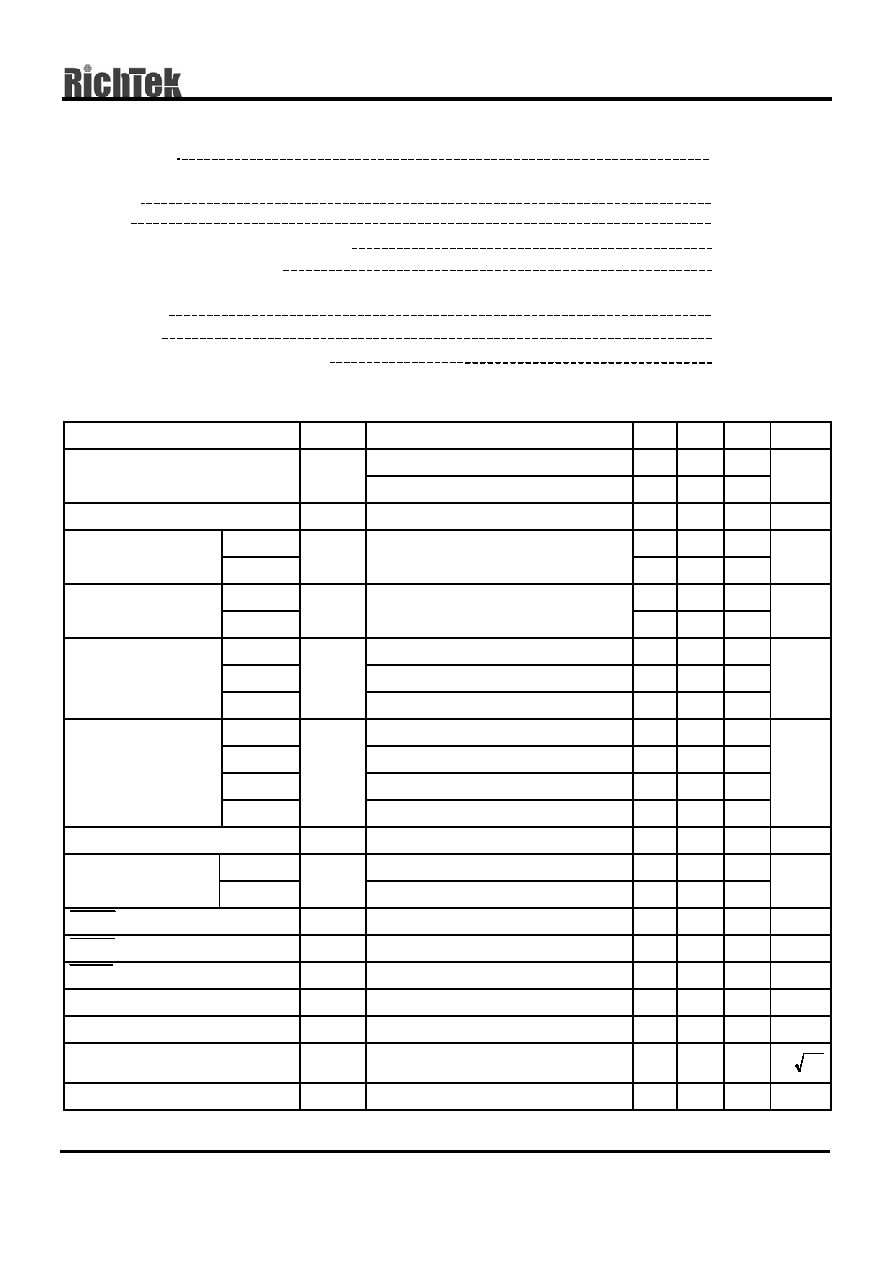
Electrical Characteristics
(V
IN
= 5.0V, C
IN
= 1
µF, C
OUT
= 1
µF, T
A
= 25
∞C, unless otherwise specified)
Parameter
Symbo
Test Conditions
Min Typ Max Units
2.9
--
7
Input Voltage Range
V
IN
I
L
= 50mA
2.7 -- 7
V
Output Voltage Accuracy
V
OUT
I
L
= 1mA
-2
--
+2
%
RT9167 200
--
--
Maximum Output
Current
RT9167A
I
MAX
500 -- --
mA
RT9167 --
300
--
Current Limit
RT9167A
I
LIMIT
R
LOAD
= 1
-- 700 --
mA
RT9167/A No
Load
--
80
150
RT9167 I
OUT
= 200mA
--
90
150
GND Pin Current
RT9167A
I
G
I
OUT
= 500mA
--
90
150
µA
RT9167/A I
OUT
= 1mA
--
1.1
5
RT9167/A I
OUT
= 50mA
--
55
100
RT9167/A I
OUT
= 200mA
--
220
300
Dropout Voltage
(Note)
(V
OUT
(Nominal)
3.0V
Version)
RT9167A
V
DROP
I
OUT
= 500mA
--
600
750
mV
Line Regulation
V
LINE
V
IN
= (V
OUT
+0.15) to 7V, I
OUT
=1mA
--
--
6
mV/V
RT9167 I
OUT
= 0mA to 200mA
--
--
25
Load Regulation
RT9167A
V
LOAD
I
OUT
= 0mA to 500mA
--
--
35
mV
SHDN Input High Threshold
V
IH
V
IN
= 3V to 5.5V
1.6
--
--
V
SHDN Input Low Threshold
V
IL
V
IN
= 3V to 5.5V
--
--
0.4
V
SHDN Bias Current
I
SD
--
--
100
nA
Shutdown Supply Current
I
GSD
V
OUT
= 0V
--
0.01
1
µA
Thermal Shutdown Temperature T
SD
--
155
--
∞C
Output Noise
e
NO
C
BP
= 10nF, C
OUT
= 10
µF
-- 350 -- nV
Hz
Ripple Rejection
PSRR F = 100Hz, C
BP
= 10nF, C
OUT
= 10
µF
-- 58 -- dB
Notes: Dropout voltage definition: V
IN
- V
OUT
when V
OUT
is 50 mV below the value of V
OUT
at V
IN
= V
OUT
+ 0.5V

RT9167/A
www.richtek.com
DS9167/A-14 June 2003
4
Typical Operating Charateristics
Output Voltage vs. Temp.
3.25
3.26
3.27
3.28
3.29
3.30
3.31
3.32
3.33
-50
-25
0
25
50
75
100
125
150
O
u
t
put
V
o
l
t
a
g
e
(
V
)
Temperature ( )
V
OUT
= 3.3V
∞C
GND Current vs. Temp.
0
15
30
45
60
75
90
105
120
-50
-25
0
25
50
75
100
125
150
Temperature ( )
G
N
D
Cu
rren
t
(
A)
∞C
µ
V
OUT
= 3.3V
Current Limit vs. Temp.
100
200
300
400
500
600
700
800
900
-50
-25
0
25
50
75
100
125
150
C
u
rre
n
t
Li
m
i
t
(m
A
)
Temperature ( )
∞C
RT9167A
V
OUT
= 3.3V
Current Limit vs. Temp.
0
60
120
180
240
300
360
420
480
-50
-25
0
25
50
75
100
125
150
C
u
rre
n
t
Li
m
i
t
(m
A
)
Temperature ( )
∞C
RT9167
PSRR
0
10
20
30
40
50
60
70
10
100
1000
10000
100000
1000000
Frequency (KHz)
PSR
R
(
d
B)
I
LOAD
= 1mA, C
OUT
= 4.7µF
V
OUT
= 3.3V, C
BP
= 10nF
10 100 1K 10K 100K 1M
Dropout Voltage vs. Output Current
0
50
100
150
200
250
300
0
25
50
75
100
125
150
175
200
Output Current (mA)
D
r
op
o
u
t
V
o
l
t
ag
e
(V
)
V
OUT
= 3.3V
85
∞C
25
∞C
-40
∞C
(mV)
RT9167/A
DS9167/A-14 June 2003
www.richtek.com
5
T
T
T
1 >
2 >
50
1
-50
60
40
20
0
-20
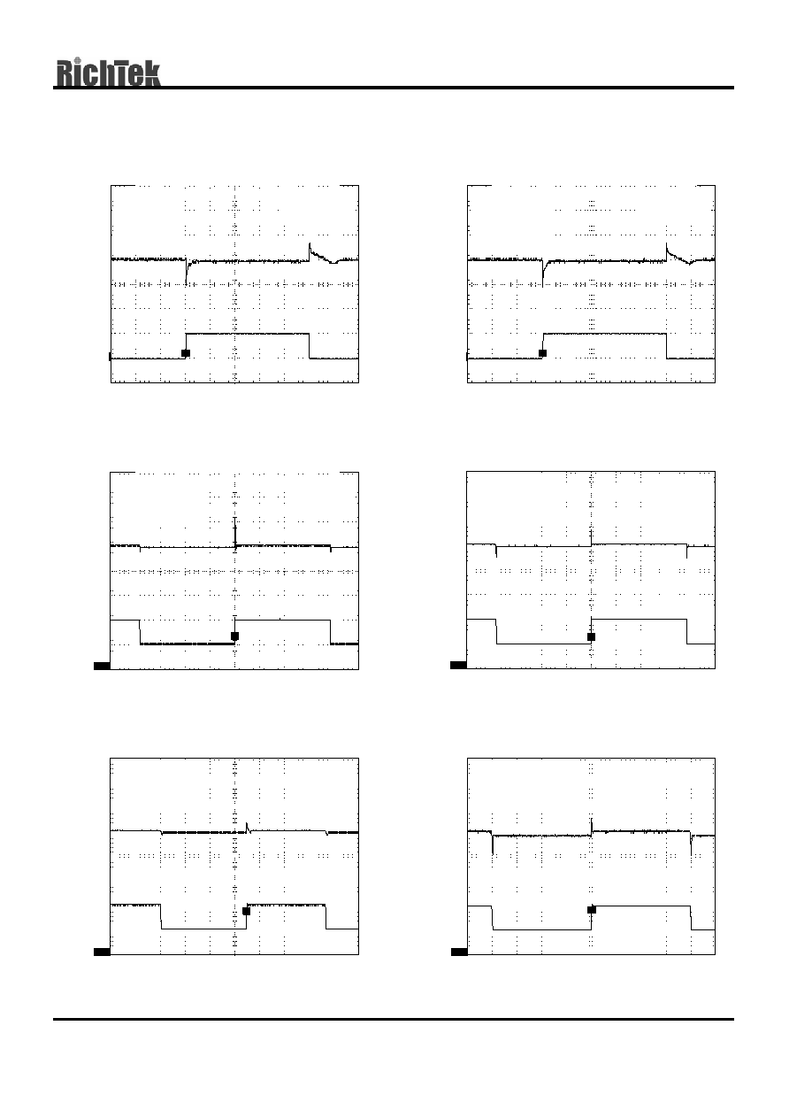
Load Transient Response
Time (50
µS/Div)
Load Current
(m
A
)
Out
put
V
o
l
t
age
Devi
at
i
on (
m
V
)
C
OUT
= 1
µF
C
IN
= 10
µF
C
BP
= 10nF
V
OUT
= 3.0V
V
IN
= 4V
T
T
T
1 >
2 >
50
1
-50
60
40
20
0
-20
Load Transient Response
Time (50
µS/Div)
Load Current
(m
A
)
Out
put
V
o
l
t
age
Devi
at
i
on (
m
V
)
C
OUT
= 4.7
µF
C
IN
= 10
µF
C
BP
= 10nF
V
OUT
= 3.0V
V
IN
= 4V
T
T
T
1
2 >
5
4
150
100
50
0
-50
Line Transient Response
Time (1mS/Div)
I
nput
V
o
l
t
age
(V
)
Out
put
V
o
l
t
age
(
m
V
)
C
OUT
= 1
µF
V
OUT
= 3.0V
Loading = 1mA
C
BP
= 10nF
T
T
T
1
2 >
5
4
150
100
50
0
-50
Line Transient Response
Time (500
µS/Div)
I
nput
V
o
l
t
age
(V
)
Out
put
V
o
l
t
age
(
m
V
)
C
OUT
= 4.7
µF
V
OUT
= 3.0V
Loading = 1mA
C
BP
= 10nF
T
T
T
1
2 >
5
4
150
100
50
0
-50
Line Transient Response
Time (1mS/Div)
I
nput
V
o
l
t
age
(V
)
Out
put
V
o
l
t
age
(
m
V
)
C
OUT
= 1
µF
V
OUT
= 3.0V
Loading = 50mA
C
BP
= 10nF
T
T
T
1
2 >
5
4
60
40
20
0
-20
Line Transient Response
Time (500
µS/Div)
I
nput
V
o
l
t
age
(V
)
Out
put
V
o
l
t
age
(
m
V
)
C
OUT
= 4.7
µF
V
OUT
= 3.0V
Loading = 50mA
C
BP
= 10nF

RT9167/A
www.richtek.com
DS9167/A-14 June 2003
6
Applications Guides
Capacitor Selection and Regulator Stability
Like any low-dropout regulator, the external capacitors
used with the RT9167/A must be carefully selected for
regulator stability and performance.
Using a capacitor whose value is > 1
µF on the
RT9167/A input and the amount of capacitance can be
increased without limit. The input capacitor must be
located a distance of not more than 0.5" from the input
pin of the IC and returned to a clean analog ground.
Any good quality ceramic or tantalum can be used for
this capacitor. The capacitor with larger value and
lower ESR (equivalent series resistance) provides
better PSRR and line-transient response.
The output capacitor must meet both requirements for
minimum amount of capacitance and ESR in all LDOs
application. The RT9167/A is designed specifically to
work with low ESR ceramic output capacitor in
space-saving and performance consideration. Using a
ceramic capacitor whose value is at least 1uF with
ESR is > 5m
on the RT9167/A output ensures
stability. The RT9167/A still works well with output
capacitor of other types due to the wide stable ESR
range. Fig.1 shows the curves of allowable ESR range
as a function of load current for various output voltages
and capacitor values. Output capacitor of larger
capacitance can reduce noise and improve
load-transient response, stability, and PSRR. The
output capacitor should be located not more than
0.5" from the V
OUT
pin of the RT9167/A and returned
to a clean analog ground.
Note that some ceramic dielectrics exhibit large
capacitance and ESR variation with temperature. It
may be necessary to use 2.2
µF or more to ensure
stability at temperatures below -10∞C in this case. Also,
tantalum capacitors, 2.2
µF or more may be needed to
maintain capacitance and ESR in the stable region for
strict application environment.
Tantalum capacitors maybe suffer failure due to surge
current when it is connected to a low-impedance
source of power (like a battery or very large capacitor).
If a tantalum capacitor is used at the input, it must be
guaranteed to have a surge current rating sufficient for
the application by the manufacture.
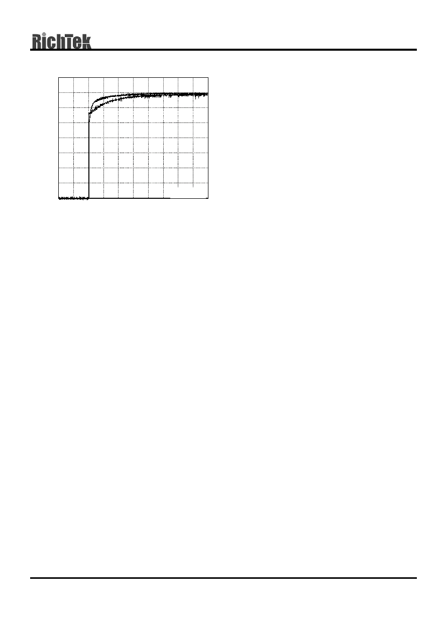
Use a 10nF bypass capacitor at BP for low output
voltage noise. The capacitor, in conjunction with an
internal 200K
resistor, which connects bypass pin
and the band-gap reference, creates an 80Hz
low-pass filter for noise reduction. Increasing the
capacitance will slightly decrease the output noise,
but increase the start-up time. The capacitor
connected to the bypass pin for noise reduction must
have very low leakage. This capacitor leakage
current causes the output voltage to decline by a
proportional amount to the current due to the voltage
drop on the internal 200K
resistor. Fig. 2 shows the
power on response.
Region of Stable Cout ESR v.s Load Current
0.001
0.01
0.1
1
10
100
0
40
80
120
160
200
Load Current (mA)
C
o
u
t E
SR
(
)
C
OUT
= 4.7
µF
C
OUT
= 1
µF
Region of Stable C
OUT
ESR vs. Load Current
0 40 80 120 160 200
C
(
)
C
OUT
ESR (
)
100
0.001
0.01
0.1
1
10
(
)
Fig. 1
Stable Region
Unstable Region
Unstable Region
RT9167/A
DS9167/A-14 June 2003
www.richtek.com
7
Load-Transient Considerations
The RT9167/A load-transient response graphs (see
Typical Operating Characteristics) show two
components of the output response: a DC shift from
the output impedance due to the load current change,
and the transient response. The DC shift is quite
small due to the excellent load regulation of the IC.
Typical output voltage transient spike for a step
change in the load current from 0mA to 50mA is tens
mV, depending on the ESR of the output capacitor.
Increasing the output capacitor's value and
decreasing the ESR attenuates the overshoot.
Shutdown Input Operation
The RT9167/A is shutdown by pulling the SHDN input
low, and turned on by driving the input high. If this
feature is not to be used, the SHDN input should be
tied to VIN to keep the regulator on at all times (the
SHDN input must not be left floating).
To ensure proper operation, the signal source used to
drive the SHDN input must be able to swing above and
below the specified turn-on/turn-off voltage thresholds
which guarantee an ON or OFF state (see Electrical
Characteristics). The ON/OFF signal may come from
either CMOS output, or an open-collector output with
pull-up resistor to the RT9167/A input voltage or
another logic supply. The high-level voltage may
exceed the RT9167/A input voltage, but must remain
within the absolute maximum ratings for the SHDN pin.
Internal P-Channel Pass Transistor
The RT9167/A features a typical 1.1
P-channel
MOSFET pass transistor. It provides several
advantages over similar designs using PNP pass
transistors, including longer battery life. The P-channel
MOSFET requires no base drive, which reduces
quiescent current considerably. PNP-based regulators
waste considerable current in dropout when the pass
transistor saturates. They also use high base-drive
currents under large loads. The RT9167/A does not
suffer from these problems and consume only 80
µA of
quiescent current whether in dropout, light-load, or
heavy-load applications.
Input-Output (Dropout) Voltage
A regulator's minimum input-output voltage
differential (or dropout voltage) determines the lowest
usable supply voltage. In battery-powered systems,
this will determine the useful end-of-life battery
voltage. Because the RT9167/A uses a P-channel
MOSFET pass transistor, the dropout voltage is a
function of drain-to-source on-resistance [R
DS(ON)
]
multiplied by the load current.
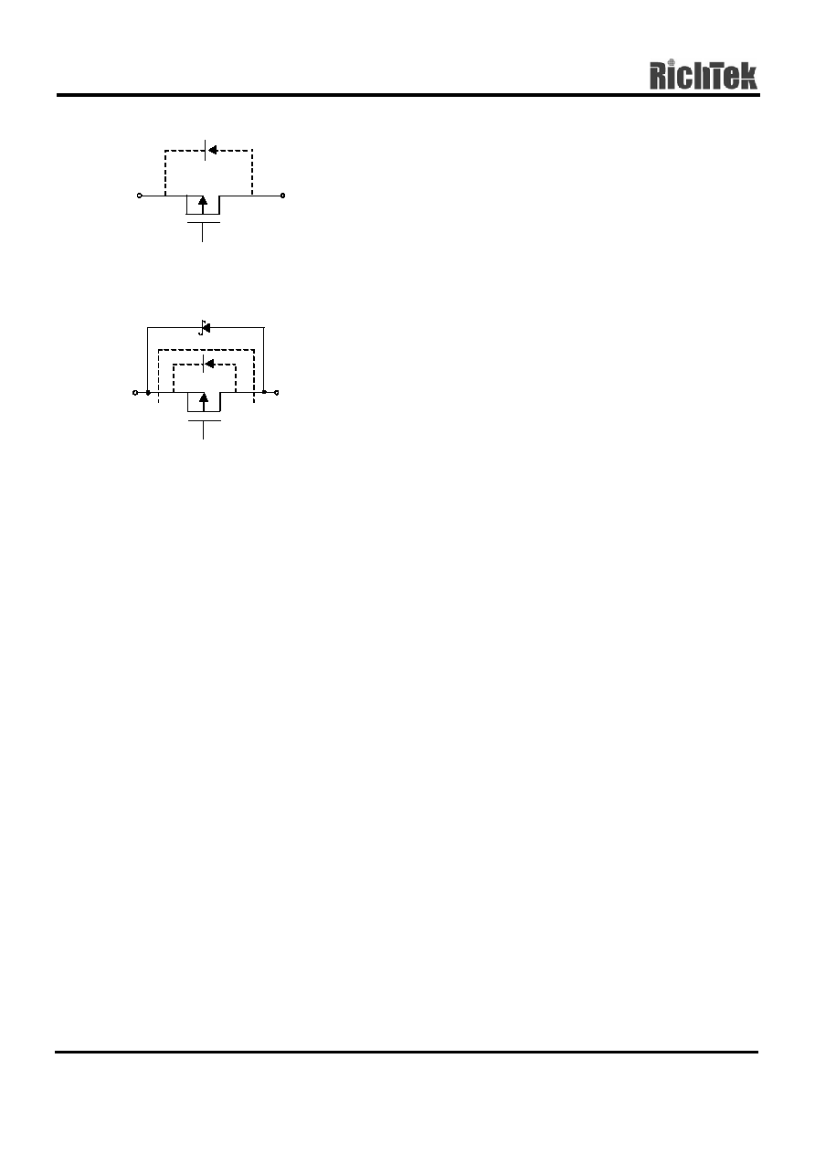
Reverse Current Path
The power transistor used in the RT9167/A has an
inherent diode connected between the regulator input
and output (see Fig.3). If the output is forced above
the input by more than a diode-drop, this diode will
become forward biased and current will flow from the
V
OUT
terminal to V
IN
. This diode will also be turned on
by abruptly stepping the input voltage to a value
below the output voltage. To prevent regulator
mis-operation, a Schottky diode should be used in
any applications where input/output voltage
conditions can cause the internal diode to be turned
on (see Fig.4). As shown, the Schottky diode is
connected in parallel with the internal parasitic diode
and prevents it from being turned on by limiting the
voltage drop across it to about 0.3V. < 100 mA to
prevent damage to the part.
10.0 15.0
0 5.0
CBP = 10nF
Time (ms)
Fig. 2
CBP = 1nF
Vo
l
t
age
(0
.
5
V
/
DIV
)
V
OUT
=3.0V
RT9167/A
www.richtek.com
DS9167/A-14 June 2003
8
Current Limit and Thermal Protection
The RT9167 includes a current limit which monitors
and controls the pass transistor's gate voltage limiting
the output current to 300mA Typ. (700mA Typ. for
RT9167A). Thermal-overload protection limits total
power dissipation in the RT9167/A. When the junction
temperature exceeds T
J
= +155∞C, the thermal sensor
signals the shutdown logic turning off the pass
transistor and allowing the IC to cool. The thermal
sensor will turn the pass transistor on again after the
IC's junction temperature cools by 10∞C, resulting in a
pulsed output during continuous thermal-overload
conditions. Thermal-overloaded protection is designed
to protect the RT9167/A in the event of fault conditions.
Do not exceed the absolute maximum
junction-temperature rating of T
J
= +150∞C for
continuous operation. The output can be shorted to
ground for an indefinite amount of time without
damaging the part by cooperation of current limit and
thermal protection.
Operating Region and Power Dissipation
The maximum power dissipation of RT9167/A depends
on the thermal resistance of the case and circuit board,
the temperature difference between the die junction
and ambient air, and the rate of airflow. The power
dissipation across the device is P = I
OUT
(V
IN
- V
OUT
).
The maximum power dissipation is: PMAX = (T
J
- T
A
)
/
JA
where T
J
- T
A
is the temperature difference between
the RT9167/A die junction and the surrounding
environment,
JA
is the thermal resistance from the
junction to the surrounding environment. The GND pin
of the RT9167/A performs the dual function of providing
an electrical connection to ground and channeling heat
away. Connect the GND pin to ground using a large
pad or ground plane.
Fig. 3
V
IN
V
OUT
Fig. 4
V
IN
V
OUT
RT9167/A
DS9167/A-14 June 2003
www.richtek.com
9
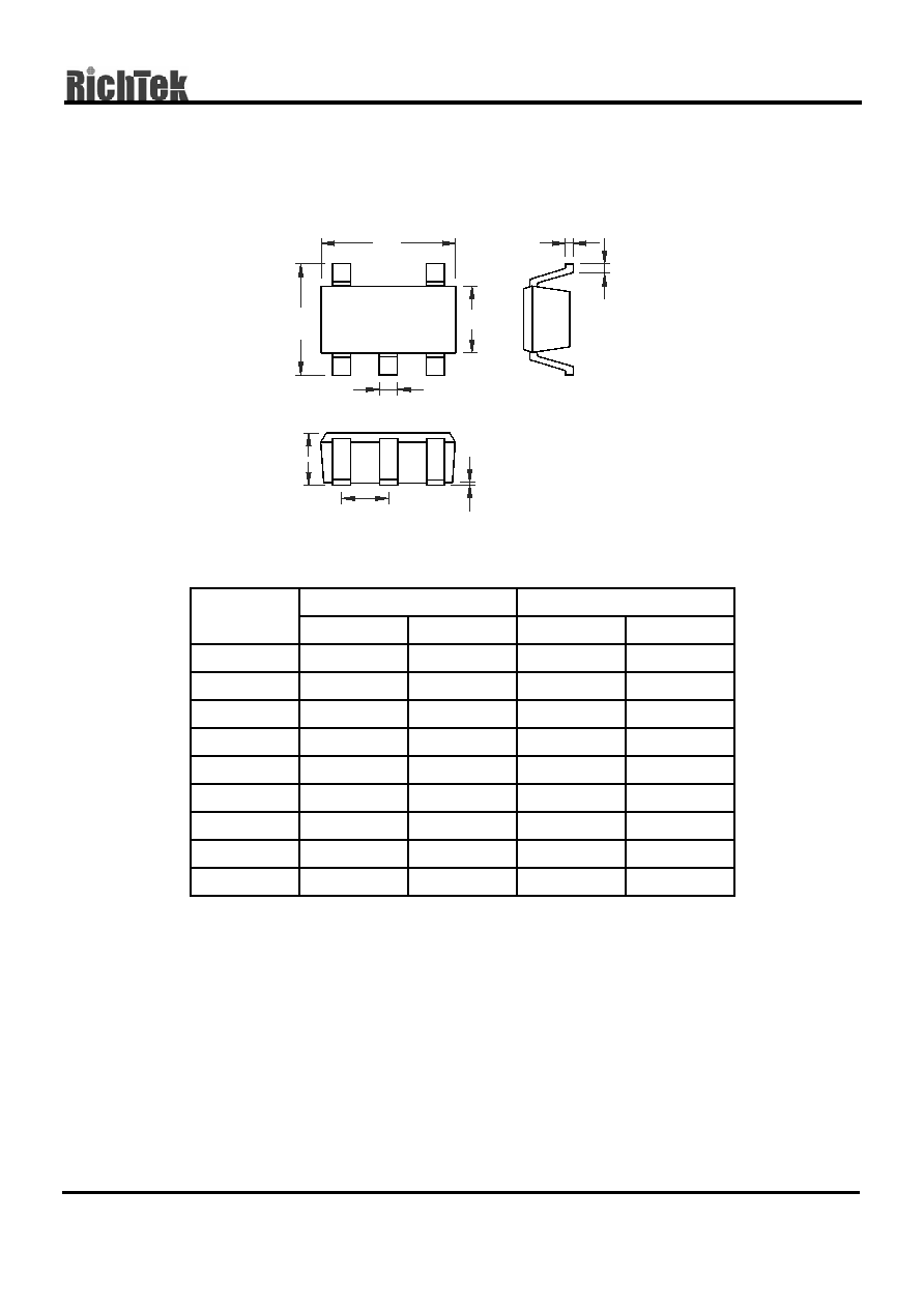
Package Information
Dimensions In Millimeters
Dimensions In Inches
Symbol
Min Max Min Max
A
0.889
1.295
0.035
0.051
A1
0.000
0.152
0.000
0.006
B
1.397
1.803
0.055
0.071
b
0.356
0.559
0.014
0.022
C
2.591
2.997
0.102
0.118
D
2.692
3.099
0.106
0.122
e
0.838
1.041
0.033
0.041
H
0.102
0.254
0.004
0.010
L
0.356
0.610
0.014
0.024
SOT- 25 Surface Mount Package
A
A1
e
b
B
D
C
H
L

RT9167/A
www.richtek.com
DS9167/A-14 June 2003
10
Dimensions In Millimeters
Dimensions In Inches
Symbol
Min Max Min Max
A
4.801
5.004
0.189
0.197
B
3.810
3.988
0.150
0.157
C
1.346
1.753
0.053
0.069
D
0.330
0.508
0.013
0.020
F
1.194
1.346
0.047
0.053
H
0.178
0.254
0.007
0.010
I
0.102
0.254
0.004
0.010
J
5.791
6.198
0.228
0.244
M
0.406
1.270
0.016
0.050
8≠Lead SOP Plastic Package
A
B
J
F
H
M
C
D
I

RT9167/A
DS9167/A-14 June 2003
www.richtek.com
11

RT9167/A
www.richtek.com
DS9167/A-14 June 2003
12
RICHTEK TECHNOLOGY CORP.
Headquarter
5F, No. 20, Taiyuen Street, Chupei City
Hsinchu, Taiwan, R.O.C.
Tel: (8863)5526789 Fax: (8863)5526611
RICHTEK TECHNOLOGY CORP.
Taipei Office (Marketing)
8F-1, No. 137, Lane 235, Paochiao Road, Hsintien City
Taipei County, Taiwan, R.O.C.
Tel: (8862)89191466 Fax: (8862)89191465
Email: marketing@richtek.com