RT9173/A
DS9173/A-09 May 2003
www.richtek.com
1
Operating temperature range
C: Commercial standard
1.5A/3A Bus Termination Regulator
General Description
The RT9173/A regulator is designed to convert
voltage supplies ranging from 1.6V to 6V into a
desired output voltage which adjusted by two
external voltage divider resistors. The regulator is
capable of sourcing or sinking up to 1.5A/3A of
current while regulating an output voltage to within
2% (DDR 1) and 3% (DDR 2) or less.
The RT9173/A, used in conjunction with series
termination resistors, provides an excellent voltage
source for active termination schemes of high speed
transmission lines as those seen in high speed
memory buses and distributed backplane designs.
The voltage output of the regulator can be used as a
termination voltage for DDR SDRAM.
Current limits in both sourcing and sinking mode,
plus on-chip thermal shutdown make the circuit
tolerant of the output fault conditions.
Ordering Information
RT9173/A
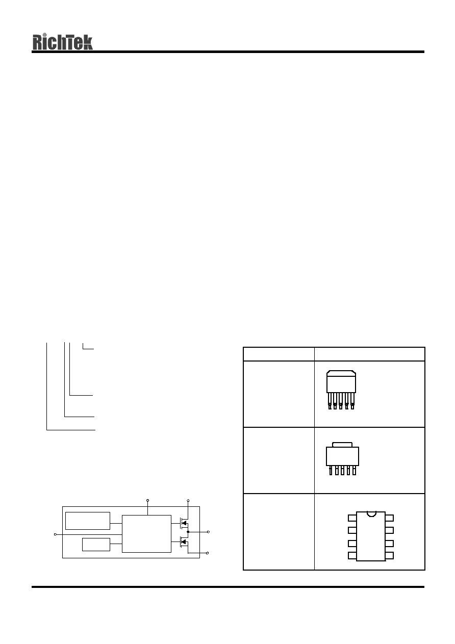
Function Block Diagram
Features
Support Both DDR 1 (1.25V
TT
) and DDR 2
(0.9V
TT
) Requirements
SOP-8, TO-252-5 and TO-263-5 Packages
Capable of Sourcing and Sinking Current 1.5A/3A
Current-limiting Protection
Thermal Protection
Integrated Power MOSFETs
Generates Termination Voltages for SSTL-2
High Accuracy Output Voltage at Full-Load
Adjustable V
OUT
by External Resistors
Minimum External Components
Shutdown for Standby or Suspend Mode
Operation with High-impedance Output
Applications
DDR Memory Termination
Active Termination Buses
Supply Splitter
Pin Configurations
Part Number
Pin Configurations
RT9173ACM5
(Plastic TO-263-5)
TOP VIEW
1. VIN
2. GND
3. VCNTL (TAB)
4. REFEN
5. VOUT
RT9173ACL5
(Plastic TO-252-5)
TOP VIEW
1. VIN
2. GND
3. VCNTL (TAB)
4. REFEN
5. VOUT
RT9173CS
(Plastic SOP-8)
TOP VIEW
Package type
M5 : TO-263-5
L5 : TO-252-5
S : SOP-8
3A sink & source
1.5A sink & source
1 2 3 4 5
1 2 3 4 5
Thermal
Current
Limiting Sensor
VOUT
REFEN
GND
CNTL
VIN
VCNTL
VIN
GND
REFEN
VOUT
VCNTL
VCNTL
VCNTL
VCNTL
1
2
3
4
8
7
6
5
RT9173/A
www.richtek.com
DS9173/A-09 May 2003
2
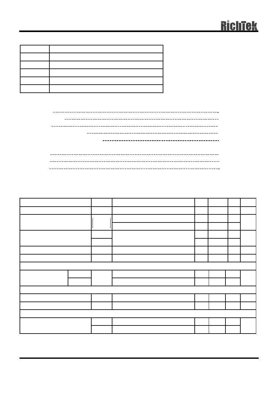
Pin Description
Pin Name
Pin Function
VIN Power
Input
GND Ground
VCNTL
Gate Drive Voltage
REFEN
Reference Voltage Input and Chip Enable
VOUT Output
Voltage
Absolute Maximum Ratings
Input Voltage
7V
Power Dissipation
Internally Limited
ESD Rating
2KV
Storage Temperature Range
-65
∞C to 150∞C
Lead Temperature (Soldering, 5 sec.)
260
∞C
Package Thermal Resistance
TO-263,
JC
7.7
∞C/W
TO-252,
JC
8
∞C/W
SOP-8,
JC
15.7
∞C/W
Electrical Characteristics
(Limits in standard typeface are for T
A
= 25
∞C, unless otherwise specified:
V
IN
= 2.5V, V
CNTL
= 3.3V, V
REFEN
= 1.25V, C
OUT
= 10
µF (Ceramic))
Parameter Symbol Test
Conditions Min
Typ
Max Units
Output Offset Voltage
V
OS
I
OUT
= 0A, Fig.1 (Note 1)
-20
0
20
mV
I
L
: 0
1.5A, Fig.1
--
0.8/1.2 2/3
Load Regulation (DDR 1/2)
V
LOAD
I
L
: 0A
-1.5A
--
0.8/1.2 2/3
%
V
IN
1.6
2.5/1.8
--
Input Voltage Range (DDR 1/2)
(Note 2)
V
CNTL
Keep V
CNTL
V
IN
on operation power
on and power off sequences
-- 3.3 6
V
Operating Current of VCNTL
I
CNTL
No
Load
-- 6.5 10
mA
Current In Shutdown Mode
I
SHDN
V
REFEN
< 0.2V, R
L
= 180
, Fig.2
--
50
90
µA
Short Circuit Protection
RT9173 Fig.3,4
2.1
--
--
Current limit
RT9173A
I
LIMIT
Fig.3,4 3.0
--
--
A
Over Temperature Protection
Thermal Shutdown Temperature T
SD
3.3V
V
CNTL
5V
125
150
--
∞C
Thermal Shutdown Hysteresis
Guaranteed by design
--
50
--
∞C
Shutdown Function
Output = High, Fig.5
0.8
--
--
Shutdown Threshold Trigger
Output = Low, Fig.5
--
--
0.2
V
Note 1: V
OS
offset is the voltage measurement defined as V
OUT
subtracted from V
REFEN
.
Note 2: For safely operate your system, the 3.3V rail MUST be tied to V
CNTL
rather than 5V rail, especially for the
new part of RT9173ACL5.
RT9173/A
DS9173/A-09 May 2003
www.richtek.com
3
Typical Application Circuit
Test Circuit
Fig.1 Output Voltage Tolerance,
V
OUT
Fig.2 Current in Shutdown Mode, I
SHCLN
R
1
= R
2
= 100K
, R
TT
= 50
/ 33 / 25
C
OUT
,
min
= 10
µF (Ceramic) + 1000µF under the worst case testing condition
R
DUMMY
= 1k
as for VOUT discharge when VIN is not present but VCNTL is present
C
SS
= 1
µF, C
IN
= 470
µF (Low ESR), C
CNTL
= 47
µF
VIN VCNTL
REFEN VOUT
GND
R
TT
V
CNTL
= 3.3V
V
IN
= 2.5V
EN
R
2
C
SS
R
1
C
IN
C
OUT
C
CNTL
RT9173/A
R
DUMMY
2N7002
VIN VCNTL
REFEN RT9173/A VOUT
GND
1.25V
2.5V
3.3V
V
OUT
C
OUT
I
L
V
VIN VCNTL
REFEN RT9173/A VOUT
GND
1.25V
2.5V
3.3V
V
OUT
C
OUT
V
R
L
A
0.2V
0V
1.25V
R
L
and C
OUT
Time delay
RT9173/A
www.richtek.com
DS9173/A-09 May 2003
4
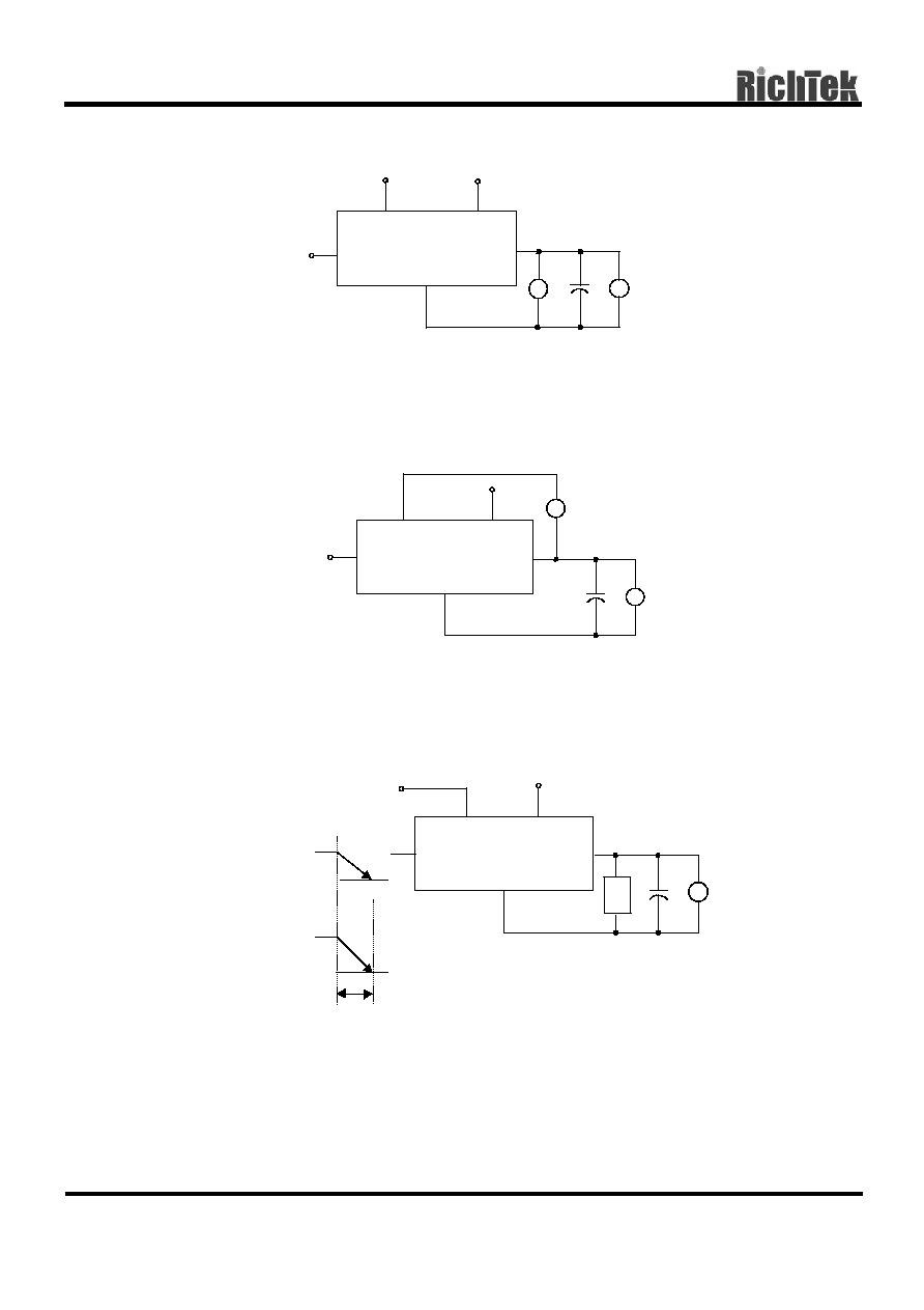
Fig.3 Current Limit for High Side, I
CLHIGH
Fig.4 Current Limit for Low Side, I
CLLOW
Fig.5 REFEN Pin Shutdown Threshold, V
TRIGGER
VIN VCNTL
REFEN RT9173/A VOUT
GND
1.25V
2.5V
3.3V
V
OUT
C
OUT
I
L
V
A
Power supply
with current limit
VIN VCNTL
REFEN RT9173/A VOUT
GND
1.25V
2.5V
3.3V
V
OUT
C
OUT
V
A
I
L
VIN VCNTL
REFEN RT9173/A VOUT
GND
2.5V
3.3V
V
OUT
C
OUT
V
R
L
0.2V
0V
1.25V
1.25V
V
OUT
V
REFEN
R
L
and C
OUT
Time delay
V
OUT
would be low if VREFEN < 0.2V
V
OUT
would be high if VREFEN > 0.8V
RT9173/A
DS9173/A-09 May 2003
www.richtek.com
5
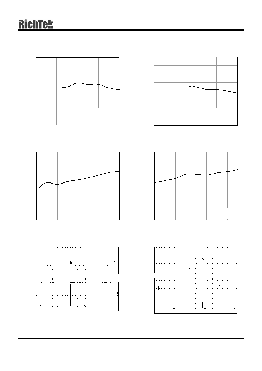
Typical Operating Characteristics
Time (250µ
S/Div)
Output Transient
Voltage (mV)
1.25V
TT
@ 1.5A Transient Response
100
50
0
-50
Output Current (A)
2
1
0
-1
-2
O
ut
pu
t
C
ur
re
nt
2
1
0
-1
-2
O
ut
pu
t
C
ur
re
nt
2
1
0
-1
-2
V
IN
= 2.5V
V
CNTL
= 3.3V
V
REFEN
= 1.25V
Swing Frequency = 1KHz
Sourcing Current (Peak) vs. Temp.
0.0
1.0
2.0
3.0
4.0
5.0
6.0
7.0
8.0
-40
-20
0
20
40
60
80
100
120
Temperature ( C)
S
o
ur
c
i
ng C
u
r
r
e
nt
(
A
)
∞
V
CNTL
= 3.3V
V
IN
= 2.5V
V
OUT
= 1.25V
Sinking Current (Peak) vs. Temp.
0.0
1.0
2.0
3.0
4.0
5.0
6.0
7.0
8.0
-40
-20
0
20
40
60
80
100
120
Temperature ( C)
S
i
n
k
i
ng C
u
r
r
e
nt
(
A
)
∞
V
CNTL
= 3.3V
V
IN
= 2.5V
V
OUT
= 1.25V
Turn-On Threshold vs. Temp.
400
450
500
550
600
650
700
-40
-20
0
20
40
60
80
100
120
Temperature ( C)
T
h
r
e
s
h
ol
d
V
o
l
t
a
g
e (
m
V
)
∞
V
CNTL
= 5.0V
V
IN
= 2.5V
Turn-On Threshold vs. Temp.
400
450
500
550
600
650
700
-40
-20
0
20
40
60
80
100
120
Temperature ( C)
T
h
r
e
s
h
ol
d
V
o
l
t
a
g
e (
m
V
)
∞
V
CNTL
= 3.3V
V
IN
= 2.5V
Time (250
µ
S/Div)
1.25V
TT
@ 3A Transient Response
100
50
0
-50
Output Current (A)
4
2
0
-2
-4
V
IN
= 2.5V
V
CNTL
= 3.3V
V
REFEN
= 1.25V
Swing Frequency = 1KHz
Output Transient
Voltage (mV)