RT9185
DS9185-02 July 2003
www.richtek.com
1
Triple, Ultra-Fast CMOS LDO Regulator
General Description
The RT9185 series are an efficient, precise triple-
channel CMOS LDO regulator specifically designed
for mother-board application. The device is intended
to powering the standby voltage in which 3.3V_PCI,
2.5V_Clock and 1.8V_ICH2 or 1.5V_ICH4 core
voltage of the PC based computer system.
Moreover, it is also optimized for CD/DVD-ROM,
CD/RW, XDSL Router or IA equipments applications.
The regulator outputs are capable of sourcing 1.5A,
0.8A and 0.3A of output current respectively.
The RT9185 also works with low-ESR ceramic
capacitors, reducing the amount of board space
necessary for power applications. The other features
include faster transient response, low dropout voltage,
high output accuracy, current limiting and thermal
shutdown protections.
The RT9185 regulators are available in fused SOP-8,
5-lead TO-252 and 5-lead TO-263 packages.
Ordering Information
RT9185
Features
Fixed Output Voltages: 3.35V at 1.5A, 2.55V at
0.8A and 1.5V or 1.8V at 0.3A
Low Quiescent Current (Typically 0.4mA)
Operating Voltage Ranges: 3.5V~5.5V
Ultra-Fast Transient Response
Tight Load and Line Regulation
Current Limiting Protection
Thermal Shutdown Protection
Only low-ESR Ceramic Capacitors Required
for Stability
Custom Voltage Available
Applications
Mother-board Power Supply
CD/DVD-ROM, CD/RW
XDSL Router
IA Equipments
Cable Modems
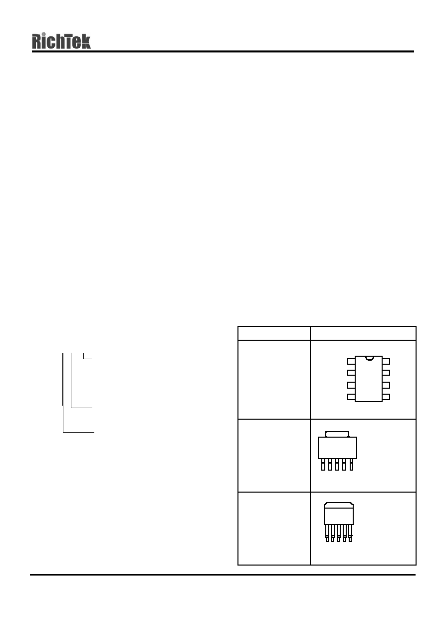
Pin Configurations
Part Number
Pin Configurations
RT9185 CS
(Plastic SOP-8)
RT9185 CL5
(Plastic TO-252-5)
TOP VIEW
1. VOUT1
2. VDD
3. GND (TAB)
4. VOUT2
5. VOUT3
RT9185 CM5
(Plastic TO-263-5)
TOP VIEW
1. VOUT1
2. VDD
3. GND (TAB)
4. VOUT2
5. VOUT3
1 2 3 4 5
Package Type
S : SOP-8
L5 : TO-252-5
M5 : TO-263-5
VOUT3
A : 1.8V
B : 1.5V
Operating Temperature Range
C: Commercial Standard
Other voltage versions please
contact RichTek for detail.
GND
GND
GND
GND
1
2
3
4
8
7
6
5
VOUT1
VDD
VOUT2
VOUT3
GND
GND
GND
GND
1
2
3
4
8
7
6
5
VOUT1
VDD
VOUT2
VOUT3
1 2 3 4 5
RT9185
www.richtek.com
DS9185-02 July 2003
2
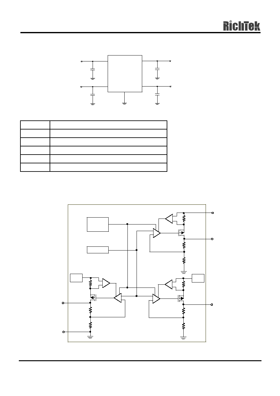
Typical Application Circuit
Pin Description
Pin Name
Pin Function
VOUT1
Channel 1 Output Voltage
VDD Supply
Input
GND Common
Ground
VOUT2
Channel 2 Output Voltage
VOUT3
Channel 3 Output Voltage
Function Block Diagram
Thermal
Sensor
Ref erence
Error Amp
+
_
+
_
+
_
+
_
+
_
+
_
VDD
VOUT1
VOUT2
VOUT3
GND
Current
Limiting
Error Amp
Error Amp
Current
Limiting
Current
Limiting
VDD
VDD
Thermal
Sensor
Ref erence
Error Amp
+
_
+
_
+
_
+
_
+
_
+
_
+
_
+
_
+
_
+
_
+
_
+
_
VDD
VOUT1
VOUT2
VOUT3
GND
Current
Limiting
Error Amp
Error Amp
Current
Limiting
Current
Limiting
VDD
VDD
GND
V
OUT1
(3.35V / 1.5A)
C2
4.7
�F
V
DD
(5VSB)
C1
2.2
�F
V
OUT3
(1.5V or 1.8V / 0.3A)
V
OUT2
(2.55V / 0.8A)
C4
1
�F
C3
4.7
�F
VOUT1
VOUT2
RT9185
VOUT3
VDD
GND
V
OUT1
(3.35V / 1.5A)
C2
4.7
�F
V
DD
(5VSB)
C1
2.2
�F
V
OUT3
(1.5V or 1.8V / 0.3A)
V
OUT2
(2.55V / 0.8A)
C4
1
�F
C3
4.7
�F
VOUT1
VOUT2
RT9185
VOUT3
VDD

RT9185
DS9185-02 July 2003
www.richtek.com
3
Absolute Maximum Ratings
(Note 1)
Supply Input Voltage
7V
Package Thermal Resistance
SOP-8
,
JC
20�C/W
TO-252-5
,
JC
10�C/W
TO-263-5,
JC
5.5�C/W
Lead Temperature (Soldering, 10 sec.)
260
�C
Junction Temperature
150
�C
Storage Temperature Range
-65�C to 150�C
ESD Susceptibility (Note 2)
HBM 2kV
MM 200V
Recommended Operating Conditions
(Note 3)
Supply Input Voltage
3.5V to 5.5V
Junction Temperature Range
-40�C to 125�C
Electrical Characteristics
(V
DD
= 5V, C
IN
= 1
�F, T
A
= 25
�C, for each LDO unless otherwise specified)
Parameter Symbol Test
Conditions Min
Typ
Max Units
V
OUT1
I
OUT
= 1mA
3.315 3.35 3.415
V
OUT2
I
OUT
= 1mA
2.525 2.55 2.60
RT9185A
1.782 1.8 1.836
Output Voltage Accuracy
V
OUT3
RT9185B
I
OUT
= 1mA
1.485 1.5 1.530
V
I
LIM1
R
LOAD
= 1
1.5
1.9
--
I
LIM2
R
LOAD
= 1
0.8
1.3
--
Current Limiting
I
LIM3
R
LOAD
= 1
0.3
0.5
--
A
Quiescent Current (triple LDOs)
(Note 5)
I
DD
I
OUT
= 0mA
-- 0.4 0.8
mA
V
DROP1
I
OUT
= 1.0A
-- 600
1085
mV
Dropout Voltage
V
DROP2
I
OUT
= 0.8A
-- 700 --
mV
Line Regulation (triple LDOs)
V
LINE
I
OUT
= 1mA, V
DD
= 4V to 6V
-- 2 10
mV
V
LOAD1
V
OUT1
, 1mA
< I
OUT
<1.0A
--
30
55
V
LOAD2
V
OUT2
, 1mA
< I
OUT
<0.8A --
30
55
Load Regulation (Note 4)
V
LOAD3
V
OUT3
, 1mA
< I
OUT
< 0.3A
--
20
45
mV
Temperature Coefficient
T
C
-- 30 --
PPM
Thermal Shutdown
T
SD
125 165 --
�C

RT9185
www.richtek.com
DS9185-02 July 2003
4
Note 1. Stresses beyond those listed under "Absolute Maximum Ratings" may cause permanent damage to the device.
These are stress ratings only, and functional operation of the device at these or any other conditions beyond those
indicated in the operational sections of the specifications is not implied. Exposure to absolute maximum rating
conditions for extended periods may affect device reliability.
Note 2. Devices are ESD sensitive. Handling precaution recommended. The human body model is a 100pF capacitor
discharged through a 1.5K
resistor into each pin.
Note 3. The device is not guaranteed to function outside its operating conditions.
Note 4. Regulation is measured at constant junction temperature by using a 20mS current pulse. Devices are tested for load
regulation in the load range from 1mA to 1.5A, 0.8A and 0.3A for each LDO respectively.
Note 5. Quiescent, or ground current, is the difference between input and output currents. It is defined by I
Q
= I
IN
� I
OUT
under no load condition (I
OUT
= 0mA). The total current drawn from the supply is the sum of the load current plus the
ground pin current.
RT9185
DS9185-02 July 2003
www.richtek.com
5
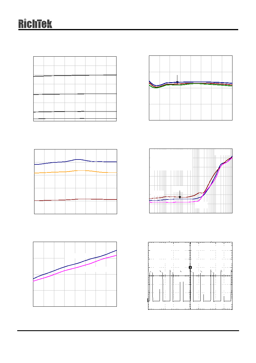
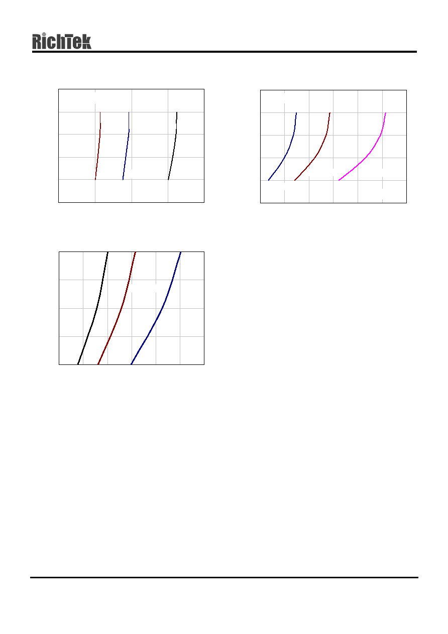
Typical Operating Characteristics
I
Load1
(A)
Short Thermal Shutdown
3
2.5
2
1.5
1
0.5
0
Time 25mS/Div
V
DD
= 5V
C
1
= 2.2
�F
T
A
= 25�C
V
DD
= 5V
V
OUT1
V
OUT2
V
OUT3
Current Limit vs. Temperature
0
0.5
1
1.5
2
2.5
-35
-15
5
25
45
65
85
105
125
Temperature ( C)
Cur
r
ent
Li
m
i
t
(
A
)
-40
(�C)
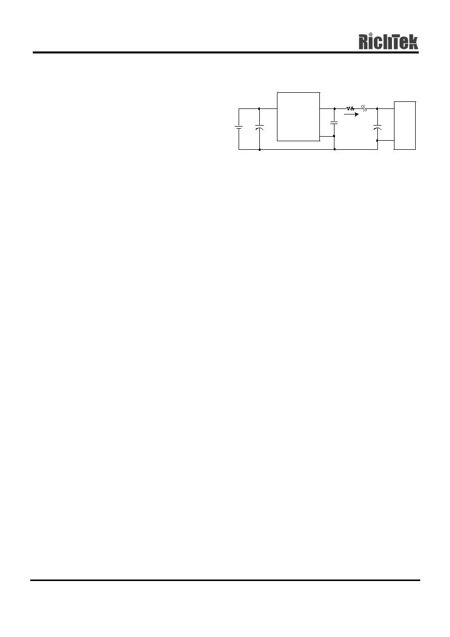
PSRR
-80
-70
-60
-50
-40
-30
-20
-10
10
100
1000
10000
100000
10000
Frequency (Hz)
PSRR (
d
B)
10 100 1K 10K 100K 1M
V
OUT1
V
OUT2
V
OUT3
V
DD
= 5V
C
1
=2.2
�F, C
2
= 4.7
�F
C
3
=4.7
�F, C
4
= 1
�F
I
O1
, I
O2
, I
O3
= 10mA
T
A
=25�C
V
DD
= 5V
Dropout Valtage vs. Temperature
0.2
0.4
0.6
0.8
1
-35
-15
5
25
45
65
85
105
125
Temperature ( C)
Dr
op
out
V
a
l
t
ag
e (
V
)
V
OUT1
= 3.3V
V
OUT2
= 2.5V
-40
(�C)
V
OUT1
= 3.3V
V
OUT2
= 2.5V
V
OUT3
= 1.8V/1.5V
Temperature Stability
1.4
1.8
2.2
2.6
3
3.4
3.8
4.2
-35
-15
5
25
45
65
85
105
125
Temperature ( C)
O
u
tp
u
t
V
o
lt
a
g
e
(V
)
-40
�
C
V
DD
= 5V
V
OUT1
V
OUT2
V
OUT3
(�C)
Quiescent Current
200
300
400
500
600
-35
-15
5
25
45
65
85
105
125
Temperature
Iq
(
�
A)
-40
RT9185
www.richtek.com
DS9185-02 July 2003
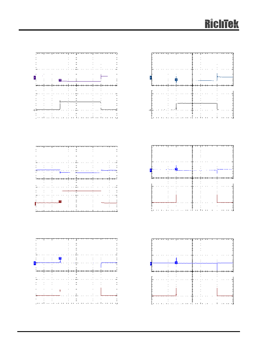
6
V
DD
=5V
V
OUT3
=1.5V
T
A
=25�C
C
1
=2.2
�
F
C
4
=1
�
F
Load Current
(mA)
Output Voltage Deviation (mV)
400
200
0
100
50
-50
0
Time 500
�
S/Div
Load Transient Response
Load Transient Response
Time 500
�
S/Div
V
DD
= 5V
V
OUT1
= 3.3V
T
A
= 25�C
C
1
= 2.2
�
F
C
2
= 4.7
�
F
Load Current
(A)
Output Voltage Deviation (mV)
1
0
100
50
-50
0
V
DD
= 5V
V
OUT2
= 2.5V
T
A
= 25�C
C
1
= 2.2
�
F
C
3
= 4.7
�
F
Load Current
(A)
Output Voltage Deviation (mV)
1
0
100
50
-50
0
Time 500
�
S/Div
Load Transient Response
V
DD
= 4.5V to 5.5V
V
OUT1
= 3.3V
T
A
= 25�C
C
1
= 2.2
�
F
C
2
= 4.7
�
F
I
OUT1
= 500mA
Input Voltage Deviation (V)
Output Voltage Deviation (mV)
5.5
4.5
10
5
-5
0
Time 100
�
S/Div
Line Transient Response
V
DD
= 4.5V to 5.5V
V
OUT2
= 2.5V
T
A
= 25�C
C
1
= 2.2
�
F
C
3
= 4.7
�
F
I
OUT1
= 400mA
Output Voltage Deviation (mV)
5.5
4.5
20
10
-10
0
Time 100
�
S/Div
Line Transient Response
Input Voltage Deviation (V)
V
DD
= 4.5V to 5.5V
V
OUT1
= 1.5V
T
A
= 25�C
C
1
= 2.2
�
F
C
4
= 4.7
�
F
I
OUT1
= 150mA
Input Voltage Deviation (V)
Output Voltage Deviation (mV)
5.5
4.5
20
10
-10
0
Time 100
�
S/Div
Line Transient Response
RT9185
DS9185-02 July 2003
www.richtek.com
7
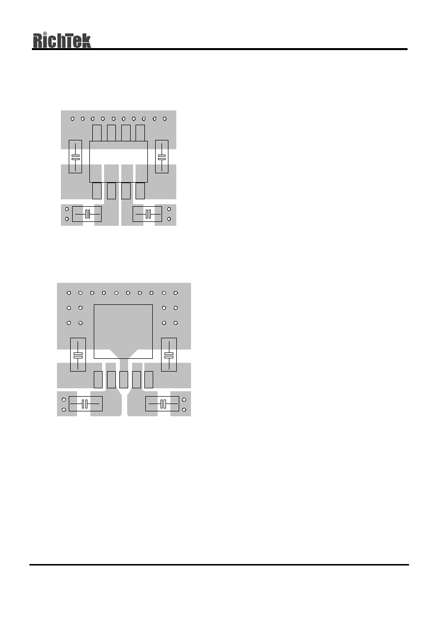
Power Dissipation vs. Copper Area
0
100
200
300
400
500
1
1.5
2
2.5
3
Power Dissipation (W)
Cop
per
A
r
ea
T
J
= 125�C
(
mm
2
)
T
A
= 65�C
T
A
= 50�C
T
A
= 25�C
SOP-8
Power Dissipation vs. Copper Area
0
100
200
300
400
500
2
2.5
3
3.5
4
4.5
5
Power Dissipation (W)
C
o
pp
er
Ar
ea
(mm
2
)
T
A
= 65�C
T
A
= 50�C
T
A
= 25�C
T
J
= 125�C
TO-252
(
mm
2
)
T
A
= 65�C
T
A
= 25�C
T
J
= 125�C
TO-263-5
Power Dissipation vs. Copper Area
100
150
200
250
300
2.5
3.5
4.5
5.5
6.5
7.5
8.5
Power Dissipation (W)
Cop
per
A
r
ea
T
A
= 50�C

RT9185
www.richtek.com
DS9185-02 July 2003
8
Applications Information
Like any low-dropout regulator, the RT9185 requires
input and output decoupling capacitors. The device is
specifically designed for portable applications
requiring minimum board space and smallest
components. These capacitors must be correctly
selected for good performance (see Capacitor
Characteristics Section). Please note that linear
regulators with a low dropout voltage have high
internal loop gains which require care in guarding
against oscillation caused by insufficient decoupling
capacitance.
INPUT CAPACITOR
An input capacitance of
2.2�F is required between
the device input pin and ground directly (the amount
of the capacitance may be increased without limit).
The input capacitor MUST be located less than 1 cm
from the device to assure input stability (see PCB
Layout Section). A lower ESR capacitor allows the
use of less capacitance, while higher ESR type (like
aluminum electrolytic) require more capacitance.
Capacitor types (aluminum, ceramic and tantalum)
can be mixed in parallel, but the total equivalent input
capacitance/ESR must be defined as above to stable
operation.
There are no requirements for the ESR on the input
capacitor, but tolerance and temperature coefficient
must be considered when selecting the capacitor to
ensure the capacitance will be
2.2�F over the entire
operating temperature range.
OUTPUT CAPACITOR
The RT9185 is designed specifically to work with
very small ceramic output capacitors. The
recommended minimum capacitance (temperature
characteristics X7R, X5R, Z5U, or Y5V) are 2.2
�F to
4.7
�F range with 10m to 50m range ceramic
capacitors between each LDO output and GND for
transient stability, but it may be increased without
limit. Higher capacitance values help to improve
transient.
The output capacitor's ESR is critical because it
forms a zero to provide phase lead which is required
for loop stability.
NO LOAD STABILITY
The device will remain stable and in regulation with
no external load. This is specially important in CMOS
RAM keep-alive applications.
INPUT-OUTPUT (DROPOUT) VOLTAGE
A regulator's minimum input-to-output voltage
differential (dropout voltage) determines the lowest
usable supply voltage. In battery-powered systems,
this determines the useful end-of-life battery voltage.
Because the device uses a PMOS, its dropout
voltage is a function of drain-to-source on-resistance,
R
DS(ON)
, multiplied by the load current:
V
DROUPOUT
= V
DD
� V
OUT
= R
DS(ON)
� I
OUT
CURRENT LIMIT
The RT9185 monitors and controls the PMOS' gate
voltage, limiting the output current to 1.9A, 1.3A and
0.5A (typ) respectively. The outputs can be shorted
to ground for an indefinite period of time without
damaging the part.
SHORT-CIRCUIT PROTECTION
The device is short circuit protected and in the event
of a peak over-current condition, the short-circuit
control loop will rapidly drive the output PMOS pass
element off. Once the power pass element shuts
down, the control loop will rapidly cycle the output on
and off until the average power dissipation causes
the thermal shutdown circuit to respond to servo the
on/off cycling to a lower frequency. Please refer to
the section on thermal information for power
dissipation calculations.
CAPACITOR CHARACTERISTICS
It is important to note that capacitance tolerance and
variation with temperature must be taken into
consideration when selecting a capacitor so that the
minimum required amount of capacitance is provided
over the full operating temperature range. In general,

RT9185
DS9185-02 July 2003
www.richtek.com
9
a good tantalum capacitor will show very little
capacitance variation with temperature, but a ceramic
may not be as good (depending on dielectric type).
Aluminum electrolytics also typically have large
temperature variation of capacitance value.
Equally important to consider is a capacitor's ESR
change with temperature: this is not an issue with
ceramics, as their ESR is extremely low. However, it
is very important in tantalum and aluminum
electrolytic capacitors. Both show increasing ESR at
colder temperatures, but the increase in aluminum
electrolytic capacitors is so severe they may not be
feasible for some applications.
Ceramic:
For values of capacitance in the 10
�F to 100�F
range, ceramics are usually larger and more costly
than tantalums but give superior AC performance for
by-passing high frequency noise because of very low
ESR (typically less than 10m
). However, some
dielectric types do not have good capacitance
characteristics as a function of voltage and
temperature.
Z5U and Y5V dielectric ceramics have capacitance
that drops severely with applied voltage. A typical
Z5U or Y5V capacitor can lose 60% of its rated
capacitance with half of the rated voltage applied to it.
The Z5U and Y5V also exhibit a severe temperature
effect, losing more than 50% of nominal capacitance
at high and low limits of the temperature range.
X7R and X5R dielectric ceramic capacitors are
strongly recommended if ceramics are used, as they
typically maintain a capacitance range within �20% of
nominal over full operating ratings of temperature
and voltage. Of course, they are typically larger and
more costly than Z5U/Y5U types for a given voltage
and capacitance.
Tantalum:
Solid tantalum capacitors are recommended for use
on the output because their typical ESR is very close
to the ideal value required for loop compensation.
They also work well as input capacitors if selected to
meet the ESR requirements previously listed.
Tantalums also have good temperature stability: a
good quality tantalum will typically show a
capacitance value that varies less than 10~15%
across the full temperature range of 125�C to
-40�C.
ESR will vary only about 2X going from the high to
low temperature limits.
The increasing ESR at lower temperatures can cause
oscillations when marginal quality capacitors are
used (if the ESR of the capacitor is near the upper
limit of the stability range at room temperature).
Aluminum:
This capacitor type offers the most capacitance for
the money. The disadvantages are that they are
larger in physical size, not widely available in surface
mount, and have poor AC performance (especially at
higher frequencies) due to higher ESR and ESL.
Compared by size, the ESR of an aluminum
electrolytic is higher than either Tantalum or ceramic,
and it also varies greatly with temperature. A typical
aluminum electrolytic can exhibit an ESR increase of
as much as 50X when going from 25�C down to
-40�C.
It should also be noted that many aluminum
electrolytics only specify impedance at a frequency of
120Hz, which indicates they have poor high
frequency performance. Only aluminum electrolytics
that have an impedance specified at a higher
frequency (between 20kHz and 100kHz) should be
used for the device. Derating must be applied to the
manufacturer's ESR specification, since it is typically
only valid at room temperature.
Any applications using aluminum electrolytics should
be thoroughly tested at the lowest ambient operating
temperature where ESR is maximum.
RT9185
www.richtek.com
DS9185-02 July 2003
10
THERMAL CONSIDERATIONS
The RT9185 is a triple channel CMOS regulator
designed to provide two output voltage from one
package. Each output pin the RT9185 can deliver a
current of up to 1.5A, 0.8A and 0.3A respectively
over the full operating junction temperature range.
However, the maximum output current must be
derated at higher ambient temperature to ensure the
junction temperature does not exceed 125
�C. With all
possible conditions, the junction temperature must be
within the range specified under operating conditions.
Each regulator contributes power dissipation to the
overall power dissipation of the package. Power
dissipation can be calculated based on the output
current and the voltage drop across each regulator.
P
D
= (V
DD
�V
OUT1
) I
OUT1
+ (V
DD
� V
OUT2
) I
OUT2
+
(V
DD
� V
OUT3
) I
OUT3
+ V
IN
I
GND
Although the device is rated for 1.5A, 0.8A and 0.3A
of output current, the application may limit the
amount of output current based on the total power
dissipation and the ambient temperature. The final
operating junction temperature for any set of
conditions can be estimated by the following thermal
equation:
P
D (MAX)
= ( T
J (MAX)
- T
A
) /
JA
Where T
J (MAX)
is the maximum junction temperature
of the die (125
�C) and T
A
is the maximum ambient
temperature.
J
A
is the thermal resistance from the
junction to the surrounding environment which is
combined with
J
C
+
CA
. Where
J
C
is junction to
case thermal resistance which for fused SOP-8 is
20�C/W, TO-252-5 is 10�C/W and TO-263-5 is
5.5�C/W,
CA
is case to ambient thermal resistance
which depend on PCB board area and air flow.
PCB LAYOUT
The RT9185 is a fixed output voltage regulator which
the voltage are sensed at the output pin. A long PCB
trace to load will cause a voltage drop between load
and RT9185. Be careful with PCB layout which
minimum the output trace length and maximum the
trace width.
The GND pin of the RT9185 performs the dual
function of providing an electrical connection to
ground and channeling heat away. Connect the GND
pin to ground using a large pad or ground plane.
Good board layout practices must be used or
instability can be induced because of ground loops
and voltage drops. The input and output capacitors
MUST be directly connected to the input, output, and
ground pins of the device using traces which have no
other currents flowing through them. The best way to
do this is to layout C
IN
and C
OUT
near the device with
short traces to the V
DD
, V
OUT
, and ground pins.
The regulator ground pin should be connected to the
external circuit ground so that the regulator and its
capacitors have a "single point ground".
It should be noted that stability problems have been
seen in applications where "vias" to an internal
ground plane were used at the ground points of the
device and the input and output capacitors. This was
caused by varying ground potentials at these nodes
resulting from current flowing through the ground
plane. Using a single point ground technique for the
regulator and it's capacitors fixed the problem. Since
high current flows through the traces going into V
IN
and coming from V
OUT
, Kelvin connect the capacitor
leads to these pins so there is no voltage drop in
series with the input and output capacitors.
Optimum performance can only be achieved when
the device is mounted on a PC board according to
the diagram below:
RT9185
VDD VOUT1
VOUT3
VOUT2
GND
GND PLANE
+
+
LOAD
TRACE RESISTANCE
RP
DROP = I
O
* RP
I
O
RT9185
VDD VOUT1
VOUT3
VOUT2
GND
GND PLANE
+
+
LOAD
TRACE RESISTANCE
RP
DROP = I
O
* RP
I
O
RT9185
DS9185-02 July 2003
www.richtek.com
11
SOP-8 Board Layout
TO-252-5/TO-263-5 Board Layout
GND
V
OUT3
GND
GND
V
DD
V
OUT2
V
OUT1
+
+
+
+
+
+
+
+
GND
GND
GND
V
DD
V
OUT2
V
OUT1
V
OUT3
RT9185
www.richtek.com
DS9185-02 July 2003
12
Package Information
Dimensions In Millimeters
Dimensions In Inches
Symbol
Min Max Min Max
A
4.801
5.004
0.189
0.197
B
3.810
3.988
0.150
0.157
C
1.346
1.753
0.053
0.069
D
0.330
0.508
0.013
0.020
F
1.194
1.346
0.047
0.053
H
0.178
0.254
0.007
0.010
I
0.102
0.254
0.004
0.010
J
5.791
6.198
0.228
0.244
M
0.406
1.270
0.016
0.050
8�Lead SOP Plastic Package
A
B
J
F
H
M
C
D
I
RT9185
DS9185-02 July 2003
www.richtek.com
13
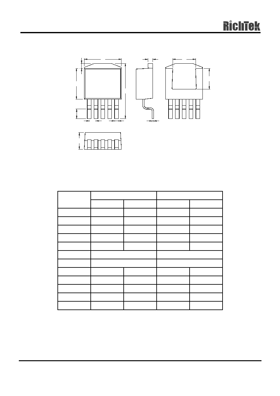
Dimensions In Millimeters
Dimensions In Inches
Symbol
Min Max Min Max
A
2.184
2.388
0.086
0.094
b 0.381
0.889
0.015 0.035
b3 4.953
5.461
0.195
0.215
C2
0.457
0.889
0.018
0.035
D 5.334
6.223
0.210
0.245
E 6.350
6.731
0.250 0.265
H 9.000
10.414
0.354
0.410
L 0.508
1.780
0.020 0.070
L2 0.508
Ref.
0.020 Ref.
L3 0.889
2.032
0.035 0.080
P
1.270 Ref.
0.050 Ref.
V 4.572 -- 0.180 --
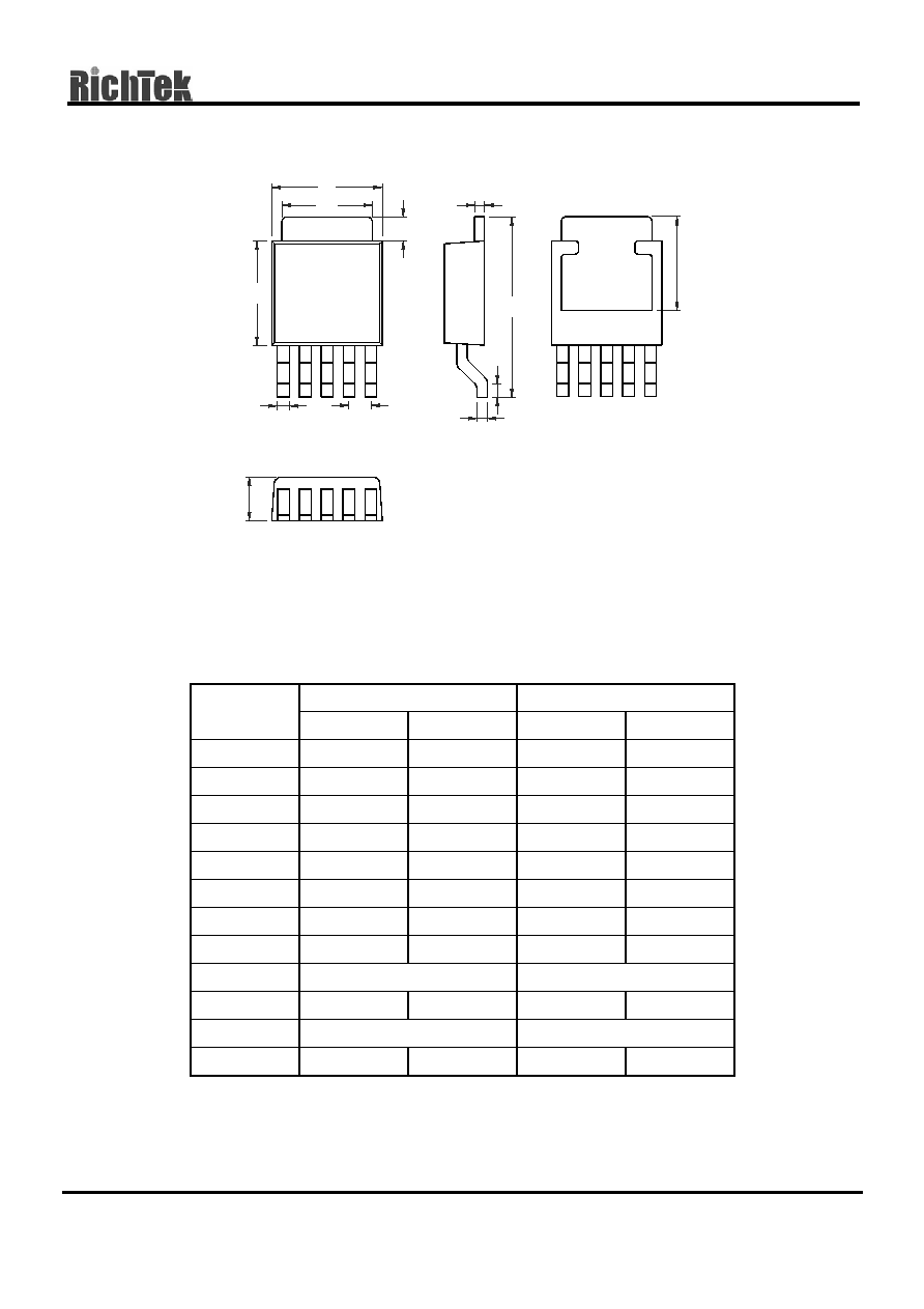
5-Lead TO-252 Plastic Package
E
P
V
H
L
L2
C2
A
L3
D
b
b3
RT9185
www.richtek.com
DS9185-02 July 2003
14
Dimensions In Millimeters
Dimensions In Inches
Symbol
Min Max Min Max
D
9.652 10.668 0.380 0.420
B 1.143 1.676 0.045 0.066
E 8.128 9.652 0.320 0.380
A 4.064 4.826 0.160 0.190
C 1.143 1.397 0.045 0.055
U
6.223 Ref.
0.245 Ref.
V
7.620 Ref.
0.300 Ref.
L1 14.605
15.875
0.575 0.625
L2 2.286 2.794 0.090 0.110
b 0.660 0.914 0.026 0.036
b2 0.305 0.584 0.012 0.023
e 1.524 1.829 0.060 0.072
5-Lead TO-263 Plastic Surface Mount Package
C
b2
A
B
E
V
U
D
e
L1
b
L2

RT9185
DS9185-02 July 2003
www.richtek.com
15

RT9185
www.richtek.com
DS9185-02 July 2003
16
RICHTEK TECHNOLOGY CORP.
Headquarter
5F, No. 20, Taiyuen Street, Chupei City
Hsinchu, Taiwan, R.O.C.
Tel: (8863)5526789 Fax: (8863)5526611
RICHTEK TECHNOLOGY CORP.
Taipei Office (Marketing)
8F-1, No. 137, Lane 235, Paochiao Road, Hsintien City
Taipei County, Taiwan, R.O.C.
Tel: (8862)89191466 Fax: (8862)89191465
Email: marketing@richtek-ic.com.tw