
Preliminary
RT9204/A
DS9204/A-02 May 2003
www.richtek.com
1
Dual Regulators - Standard Buck PWM DC-DC and
Linear Controller
General Description
The RT9204/A is a dual power controllers designed
for high performance graphics cards and computer
applications. The IC integrates a standard buck
controller, a linear regulator driver and protection
functions into a small 8-pin package.
The RT9204/A uses an internal compensated voltage
mode PWM control for simple application design. An
internal 0.8V reference allows the output voltage to
be precisely regulated to low voltage requirement. A
fixed 600kHz oscillator reduce the component size
for saving board area.
The RT9204/A protects the converter and regulator
by monitoring the output under voltage.
Applications
Motherboard Power Regulation for Computers
Subsystems Power Supplies
Cable Modems, Set Top Box, and DSL Modems
DSP and Core Communications Processor Supplies
Memory Power Supplies
Personal Computer Peripherals
Industrial Power Supplies
5V-Input DC-DC Regulators
Low Voltage Distributed Power Supplies
Features
Operate from 5V
0.8V Internal Reference
Voltage Mode PWM Control
Fast Transient Response
Fixed 600kHz Oscillator Frequency
Full 0~100% Duty Cycle
Internal Soft Start
Internal PWM Loop Compensation
Pin Configurations
Part Number
Pin Configurations
RT9204/ACS
(Plastic SOP-8)
TOP VIEW
Ordering Information
RT9204/A
GND
VCC
DRV
FBL
UGATE
BOOT
SD
FB
1
2
3
4
8
7
6
5
Operating Temperature Range
C : Commercial Standard
Package Type
S : SOP-8
UVP : Hiccup Mode
UVP : Latch Mode

RT9204/A
Preliminary
www.richtek.com
DS9204/A-02 May 2003
2
Typical Application Circuit
Fig.1 RT9204/A powered from 5V only
Fig.2 RT9204/A powered from 12V
VCC
DRV
UGATE
BOOT
GND
SD
RT9204/A
5
8
7
6
1
3
FB
R4
100
+
C6
220uF
V
OUT2
1.6V
1uF
3.3V
Q1
2SD1802
C3
0.1uF
BAT54A
R3
250
R2
120
C7
10nF
FBL
R5
100
+
L1
5uH
C4
1000uF
2.5V
V
OUT1
MU
C2
1uF
+
C1
470uF
R1
2.2
5V
C5
V
AUX
4
2
D1
SS34
VCC
DRV
UGATE
BOOT
GND
SD
RT9204/A
5
8
7
6
1
3
FB
R4
100
+
C6
220uF
V
OUT2
1.6V
3.3V
Q1
2SD5706
R3
250
R2
120
C7
10nF
FBL
R5
100
+
L1
5uH
C4
1000uF
2.5V
V
OUT1
MU
C2
1uF
+
C1
470uF
R6
10
12V
V
AUX
4
2
D1
SS34
Suggest use Transistor
C7
1uF
R1
5V
C5
1uF
5V
2.2

Preliminary
RT9204/A
DS9204/A-02 May 2003
www.richtek.com
3
Layout Placement
Layout Notes
1. Put C
1
& C
2
to be near the MU drain and ML source nodes.
2. Put RT9204/A to be near the C
OUT
3. Put C
BOOT
as close as to BOOT pin
4. Put C
VCC
as close as to VCC pin
Function Block Diagram
6.0V
Regulator
Control
Logic
Power
on Reset
Soft Start
0.8V
Reference
600kHz
Oscillator
_
+
_
35dB
+
_
UVP
+
_
OVP
VCC
FB
GND
BOOT
UGATE
Error Amp
0.8V
1V
+
_
UVP
_
LDO
+
+
+
PWM
+
SS
DRV
FBL
0.5V
+
GND
BOOT
RT9204/A
VCC
C
VCC
1
�F
C
OUT
1000
�F
+
G
S
MU
D
Diode
C
BO OT
0.1
�F
L
5
�H
C1
1
�F
C2
470
�F
GND Return
RT9204/A
Preliminary
www.richtek.com
DS9204/A-02 May 2003
4
Absolute Maximum Ratings
Supply Voltage VCC
7V
BOOT & UGATE to GND
15V
Input, Output or I/O Voltage
GND
-0.3V ~ 7V
Power Dissipation, P
D
@ T
A
= 25
�C
SOP-8
0.625W
Package Thermal Resistance
SOP-8,
JA
160
�C/W
Ambient Temperature Range
0
�C ~ +70�C
Junction Temperature Range
-40
�C ~ +125�C
Storage Temperature Range
-65
�C ~ +150�C
Lead Temperature (Soldering, 10 sec.)
260
�C
CAUTION:
Stresses beyond the ratings specified in "Absolute Maximum Ratings" may cause permanent damage to the device.
This is a stress only rating and operation of the device at these or any other conditions above those indicated in the
operational sections of this specification is not implied.
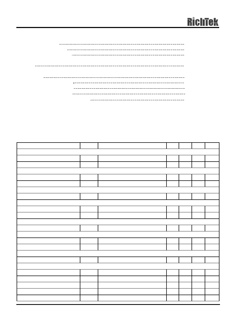
Electrical Characteristics
(V
CC
= 5V, T
A
= 25
�C, Unless otherwise specified.)
Parameter Symbol
Test
Conditions Min
Typ
Max
Units
VCC Supply Current
Nominal Supply Current
I
CC
UGATE, LGATE open
--
3
--
mA
VCC Regulated Voltage
V
CC
V
BOOT=
12V --
6
--
V
Power-On Reset
Rising VCC Threshold
3.75
4.1
4.35
V
VCC Threshold Hysteresis
--
0.5
--
V
Reference
Reference Voltage
Both FB & FBL
0.784 0.8 0.816
V
Oscillator
Free Running Frequency
550
600
650
KHz
Ramp Amplitude
V
OSC
--
1.75
--
V
P-P
PWM Error Amplifier
DC Gain
--
35
--
dB
PWM Controller Gate Driver
Upper Drive Source
R
UGATE
V
BOOT
= 12V; V
BOOT
- V
UGATE
= 1V
-- 7 --
Upper Drive Sink
R
UGATE
V
UGATE
= 1V
-- 5 --
Linear Regulator
DRV Driver Source
V
DRV
= 2V
100 -- -- mA
Protection
FB Over-Voltage Trip
FB Rising
--
1
--
V
FB & FBL Under-Voltage Trip
FB & FBL Falling
--
0.5
--
V
Soft-Start Interval
--
1
--
mS
SD Pin Threshold
VCC = 5V
--
1.5
--
V
SD pin Sink Current
VCC = 5V
--
40
--
�A

Preliminary
RT9204/A
DS9204/A-02 May 2003
www.richtek.com
5
Typical Operating Characteristics
Load Transient
Time
UGATE
V
CC
= 5V
V
OUT
= 2.2V
C
OUT
= 3000
�F
V
OUT
Load Transient
Time
UGATE
V
CC
= 5V
V
OUT
= 2.2V
C
OUT
= 3000
�F
V
OUT
Power On
Time
V
CC
V
CC
= 5V
V
OUT
= 2.2V
V
OUT1
V
OUT2
Power Off
Time
V
CC
V
CC
= 5V
V
2 2V
V
OUT1
V
OUT2
Short Hiccup
Time (2ms/Div)
V
OUT
V
CC
= 5V
V
OUT
= 2.2V
UGATE
RT9204A
Short Hiccup (Latch Mode)
Time (5ms/Div)
V
OUT
V
CC
= 5V
V
OUT
= 2.2V
UGATE
RT9204