Preliminary
RT9205/A
DS9205/A-03 May 2003
www.richtek.com
1
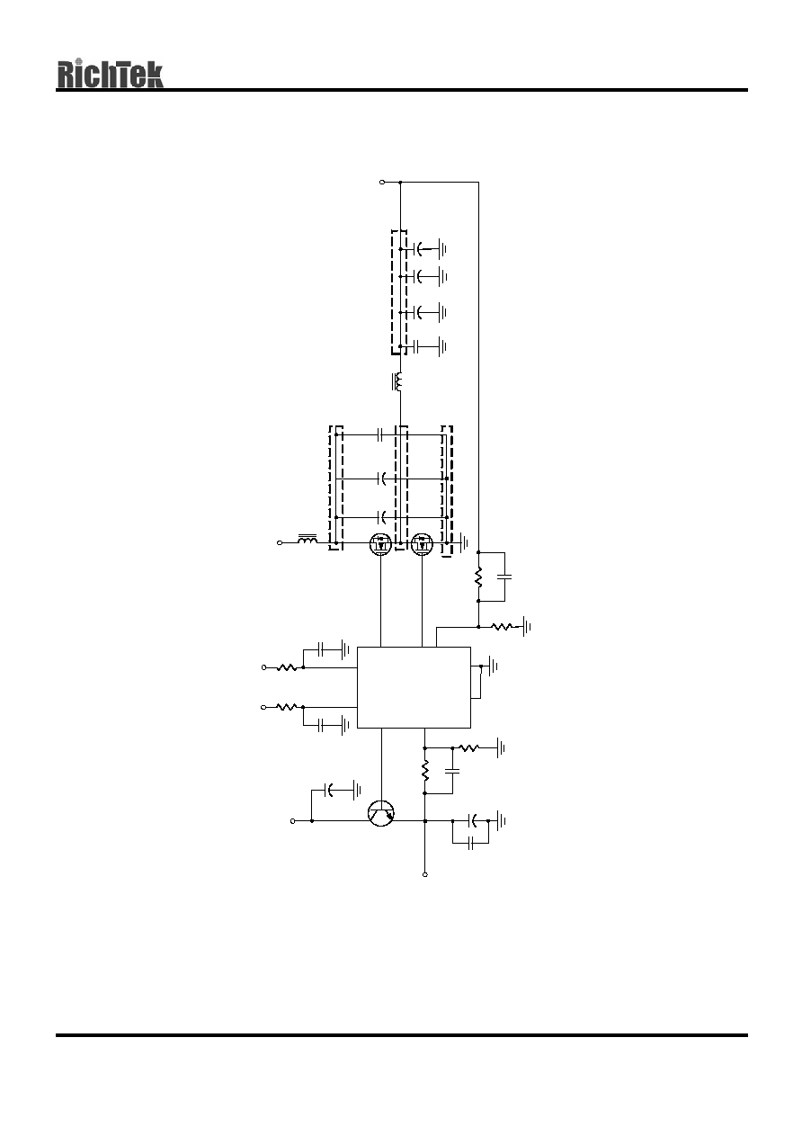
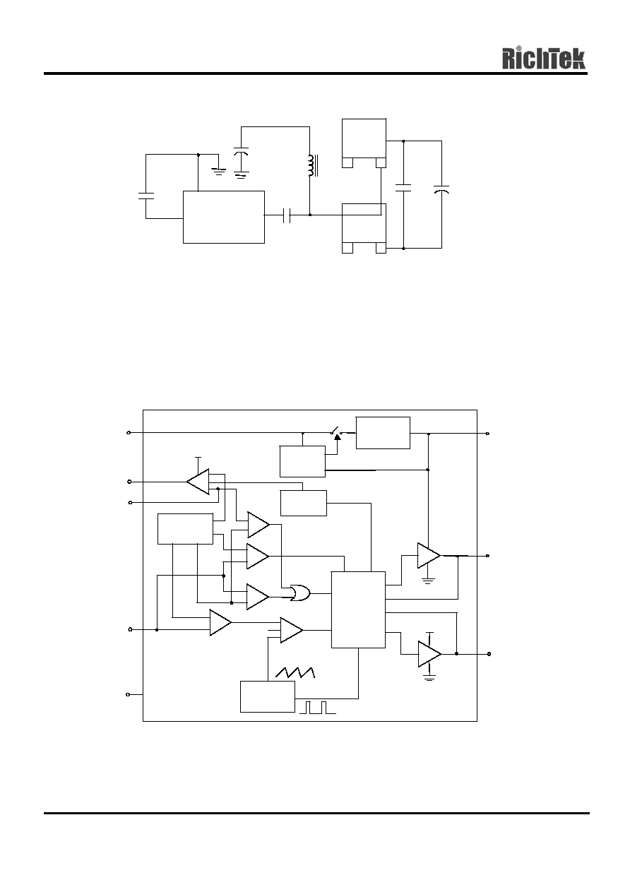
Dual Regulators - Synchronous Buck PWM DC-DC and
Linear Controller
General Description
The RT9205/A is a dual-output power controllers
designed for high performance graphics cards and
personal computers. The IC integrates a
synchronous buck controller, a linear controller and
protection functions into a small 14-pin package.
The RT9205/A uses an internal compensated voltage
mode PWM control for simplying design. An internal
0.8V reference allows the output voltage to be
precisely regulated to meet low output voltage
requirement. A fixed 300kHz oscillation frequency
reduces the component size for saving board area.
The RT9205/A also features over voltage protection
(OVP) and under voltage lock-out (UVLO).
Applications
PC Motherboard
Cable Modems, Set-Top-Box, and XDSL Modems
DSP and Core Communications Processor Supplies
Memory Power Supplies
Personal Computer Peripherals
Industrial Power Supplies
5V Input DC-DC Regulators
Low Voltage Distributed Power Supplies
Graphic Cards
Features
Operates at 5V
0.8V Internal Reference
Drives Two N-channel MOSFET
Voltage Mode PWM Control
Fast Transient Response
Fixed 300kHz Oscillator Frequency
Dynamic 0~100% Duty Cycle
Internal PWM Loop Compensation
Internal Soft-Start
Adaptive Non-overlapping Gate Driver
Over-voltage Protection Uses Lower MOSFET
Pin Configurations
Part Number
Pin Configurations
RT9205/ACS
(Plastic SOP-14)
TOP VIEW
Ordering Information
RT9205/A
LGATE
PGND
GND
VCC
1
2
3
4
14
13
12
11
UGATE
BOOT
NC
NC
DRV
FBL
NC
5
6
7
10
9
8
NC
FB
NC
Operating Temperature Range
C : Commercial Standard
Package Type
S : SOP-14
UVP : Hiccup Mode
UVP : Latch Mode

Preliminary
RT9205/A
DS9205/A-03 May 2003
www.richtek.com
5
Absolute Maximum Ratings
Supply Voltage VCC
7V
BOOT & UGATE to GND
19V
Input, Output or I/O Voltage
GND
-0.3V ~ 7V
Package Thermal Resistance
SOP-14,
JA
160
�C/W
Ambient Temperature Range
0
�C ~ +70�C
Junction Temperature Range
-40
�C ~ +125�C
Storage Temperature Range
-65�C ~ +150�C
Lead Temperature (Soldering, 10 sec.)
260
�C
CAUTION:
Stresses beyond the ratings specified in "Absolute Maximum Ratings" may cause permanent damage to the device.
This is a stress only rating and operation of the device at these or any other conditions above those indicated in the
operational sections of this specification is not implied.
Electrical Characteristics
(V
CC
= 5V, T
A
= 25
�C, Unless otherwise specified.)
Parameter Symbol
Test
Conditions
Min
Typ
Max
Units
VCC Supply Current
Nominal Supply Current
I
CC
UGATE, LGATE open
--
3
--
mA
VCC Regulated Voltage
I
CC
V
BOOT
= 12V
5
6
7
V
Power-On Reset
Rising VCC Threshold
3.8
4.1
4.4
V
VCC Threshold Hysteresis
--
0.5
--
V
Reference
Reference Voltage
V
FB
Both PWM and linear regulator
0.784 0.8 0.816
V
Oscillator
Free Running Frequency
250
300
350
KHz
Ramp Amplitude
V
OSC
-- 1.75 -- V
P-P
PWM Error Amplifier
DC gain
32
35
38
dB
PWM Controller Gate Driver
Upper Drive Source
R
UGATE
BOOT= 12V
BOOT-V
UGATE
= 1V
-- 7.5 11
Upper Drive Sink
R
UGATE
V
UGATE
= 1V
--
5
8
Lower Drive Source
R
LGATE
VCC - V
LGATE
= 1V,
--
3.5
6
Lower Drive Sink
R
LGATE
V
LGATE
= 1V
--
2
5
Linear Regulator
DRV Driver Source
V
DRV
= 2V
100
--
--
mA
Protection
FB Over-Voltage Trip
FB Rising
0.9
1
--
V
FB & FBL Under-Voltage Trip
FB & FBL Falling
--
0.5
0.65
V
Soft-Start Interval
--
2.5
--
mS