 | –≠–ª–µ–∫—Ç—Ä–æ–Ω–Ω—ã–π –∫–æ–º–ø–æ–Ω–µ–Ω—Ç: RT9262/A | –°–∫–∞—á–∞—Ç—å:  PDF PDF  ZIP ZIP |

Preliminary
RT9262/A
DS9262/A-05 October 2002
www.richtek.com
1
High Efficiency, Low Supply Current,
Step-up DC/DC Converter
General Description
The RT9262/A is a compact, high efficient, step-up
DC/DC converter with an adaptive current mode
PWM control loop, providing a stable and high
efficient operation over a wide range of load
currents. It operates in both continuous and
discontinuous current modes in stable waveforms
without external compensation.
The low start-up input voltage below 1V makes
RT9262/A suitable for 1 to 4 battery cell applications
providing up to 400mA output current. The 550KHz
high switching rate minimized the size of external
components. Besides, the 17
µA low quiescent
current together with high efficiency maintains long
battery lifetime.
The 1.8V to 5V output voltage is set with 2 external
resistors. Both internal 2A switch and driver for
driving external power devices (NMOS or NPN) are
provided.
A 300mA LDO is included in RT9262 to provide a
secondary low noise output as well as an output
current stop in the shutdown mode. Similarly, a 1.8V
to 5V LDO output voltage can be set with 2 external
resistors. For RT9262A, a low battery detector with
0.86V detection voltage is included. RT9262/A are
provided in SOP-8 packages.
Ordering Information
RT9262A
Features
1.0V Low Start-up Input Voltage
High Supply Capability to Deliver 3.3V 100mA
with 1V Input Voltage
17
µA Quiescent (Switch-off) Supply Current
90% Efficiency
550KHz Fixed Switching Rate
Providing Flexibility for Using Internal and
External Power Switches
Built-in 300mA LDO, also for the Zero-Output-
Current Shutdown Mode (RT9262)
Boost DC-DC Integrating LDO for Up-Down
Regulation (RT9262)
Built-in 0.86V Voltage Detector (RT9262A)
8-Pin SOP Package
Applications
PDA
Portable Instrument
Wireless Equipment
DSC
LCD Back Bias Circuit
RF-Tags
Pin Configurations
Part Number
Pin Configurations
RT9262CS
(Plastic SOP-8)
TOP VIEW
RT9262ACS
(Plastic SOP-8)
TOP VIEW
Operating temperature range
C: Commercial standard
Package type
S : SOP-8
A : Include low battery detector
Default : Include LDO
GND
EXT
LFB
LDOO
CE
LX
VDD
FB
1
2
3
4
8
7
6
5
GND
EXT
LBO
LBI
CE
LX
VDD
FB
1
2
3
4
8
7
6
5

RT9262/A
Preliminary
www.richtek.com
DS9262/A-05 October 2002
2
Marking Information
Part Number
Marking
RT9262CS RT9262CS
RT9262ACS
RT9262ACS
Typical Application Circuit
Fig. 1 RT9262 Typical Application for Portable Instruments below 400mA
Fig. 2 RT9262A Typical Application for Portable Instruments below 400mA
C1
100
µF
VDD
CE
RT9262
EXT
LDO O LX
L F B G N D F B
+
3.3V
V
OUT1
C2
1
µF
D1
L1
4.7
µH
R1
1.6M
R2
980K
R4
1.3M
R3
680K
C3
10
µF
2.5V
V
OUT2
V
IN
100pF
1nF
+
100
µF
VDD
CE
RT9262A
EXT
LB O LX
L B I G N D F B
+
3.3V
V
OUT1
C2
1
µF
D1
L1
4.7
µH
R1
1.6M
R2
980K
R4
R3
Low Battery
Warning Output
(Open Collector)
V
IN
100pF
C1
100
µF
100
µF

Preliminary
RT9262/A
DS9262/A-05 October 2002
www.richtek.com
3
Fig. 3 Application Circuit with Zero-Output-Current Shutdown Mode Control
Fig. 4 0.4A ~ 2A Output Current Application
Fig. 5 High Voltage Application (Rm should be added when IL > 100mA)
C1
100
µF
VDD
CE
RT9262
EXT
LDO O LX
L F B G N D F B
+
C2
1
µF
D1
L1
4.7
µH
R1
1.6M
R2
980K
C3
10
µF
3.3V
V
OUT
V
IN
100pF
Chip Enable Input
+
100
µF
C1
100
µF
VDD
CE LX
LDOO EXT
LF B G ND F B
+
3.3V
V
OUT1
C2
1
µF
D1
L1
4.7
µH
R1
1.6M
R2
980K
R4
1.3M
R3
680K
C3
10
µF
2.5V
V
OUT2
V
IN
100pF
1nF
Q1
NMOS
+
RT9262
100
µF
VDD
CE
RT9262
EXT
LDO O LX
LF B G ND F B
R4
1.3M
R3
680K
C3
10
µF
2.5V
V
OUT2
1nF
C1
100
µF
+
C2
1
µF
D1
R1
2.2M
R2
200K
Q1
NMOS
5V
V
IN
15V
V
OUT1
0.1
µF
Rm
0.05 ~0.1
L1
10
µH
+
100
µF

RT9262/A
Preliminary
www.richtek.com
DS9262/A-05 October 2002
4
Pin Description
Pin No.
RT9262 RT9262A
Pin Name
Pin Function
1 1
GND
Ground
2 2
EXT
Output pin for driving external NMOS or NPN
When driving an NPN, a resistor should be added for limiting base current.
3 --
LFB Feedback pin of the built-in LDO (Internal Vref = 0.86V)
4 --
LDOO
Voltage output pin of the built-in LDO
-- 3
LBO
Drain output pin of the NMOS of the built-in low voltage detector
This pin will be internally pulled low when the voltage at LBI pin drops to
below 0.86V.
-- 4
LBI
Input pin of the built-in low voltage detector
Trip point = 0.86V
5 5
FB
Feedback input pin
Internal reference voltage for the error amplifier is 1.25V.
6 6
VDD
Input positive power pin of RT9262/A
7 7
LX Pin for switching
8 8
CE
Chip enable
RT9262/A gets into shutdown mode when CE pin set to low.
Absolute Maximum Ratings
Supply Voltage
-0.3V to 7V
LX Pin Switch Voltage
-0.3V to 7V
LDO Output Voltage
-0.3V to (VDD + 0.3V)
Other I/O Pin Voltages
-0.3V to (VDD + 0.3V)
LX Pin Switch Current
2.5A
EXT Pin Driver Current
30mA
LBO Current
30mA
Power Dissipation, P
D
@ T
A
= 25
∞C
SOP-8
0.625W
∑ Package Thermal Resistance
SOP-8,
JA
160
∞C/W
Operating Junction Temperature
150
∞C
Storage Temperature Range
-65
∞C ~ +150∞C
Preliminary
RT9262/A
DS9262/A-05 October 2002
www.richtek.com
5
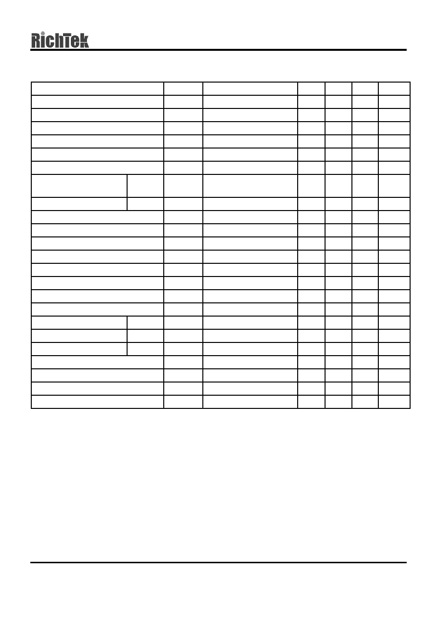
Electrical Characteristics
(V
IN
= 1.5V, VDD set to 3.3V, Load Current = 0, T
A
= 25
∞C, unless otherwise specified)
Parameter Symbol
Test
Conditions
Min
Typ
Max
Units
Start-UP Voltage
V
ST
I
L
= 1mA
-- 0.98
1.05
V
Operating VDD Range
V
DD
Start-up to I
DD1
> 250µA
0.8 -- 6.5
*
V
No Load Current I (V
IN
)
I
NO LOAD
V
IN
= 1.5V, V
OUT
= 3.3V
-- 47 --
µA
Switch-off Current I (VDD)
I
SWITCH OFF
V
IN
= 6V
-- 17 --
µA
Shutdown Current I (V
IN
)
I
OFF
CE Pin = 0V, V
IN
= 4.5V
-- 0.1 1
µA
Feedback Reference Voltage
V
REF
Close Loop, VDD = 3.3V
1.225 1.25 1.275
V
Feedback Reference
Voltage for LDO
RT9262
V
REF
Close Loop, VDD = 3.3V
0.843 0.86 0.877
V
LBI Pin Trip Point
RT9262A
VDD = 3.3V
0.843 0.86 0.877
V
Switching Rate
F
S
VDD = 3.3V
-- 550 -- KHz
Maximum Duty
D
MAX
VDD = 3.3V
-- 92 -- %
LX
ON Resistance
VDD = 3.3V
-- 0.25 --
Current Limit Setting
I
LIMIT
VDD = 3.3V
-- 2 -- A
EXT ON Resistance to VDD
VDD = 3.3V
-- 40 --
EXT ON Resistance to GND
VDD = 3.3V
-- 30 --
Line Regulation
V
LINE
V
IN
= 1.5 ~ 2.5V, I
L
= 1mA
-- 10 -- mV/V
Load Regulation
V
LOAD
V
IN
= 2.5V, I
L
= 1 ~ 100mA
-- 0.25 -- mV/mA
LDO PMOS ON Resistance RT9262
VDD = 3.3V
-- 1 1.5
LDO Drop Out Voltage
RT9262
V
DROP
VDD = 3.3V, IL = 100mA
-- 70 -- mV
LBO ON Resistance
RT9262A
VDD = 3.3V
-- 40 --
CE Pin Trip Level
VDD = 3.3V
0.2 0.8 1.4 V
Temperature Stability for FB, LFB, LBI T
S
Guaranteed by Design
--
50
--
ppm/∞C
Thermal Shutdown
T
SD
Guaranteed by Design
--
165
--
∞C
Thermal Shutdown Hysterises
T
SD
Guaranteed by Design
--
10
--
∞C
* Note: The CE pin shall be tied to VDD pin and inhibit to act the ON/OFF state whenever the VDD pin voltage
may reach to 5.5V or above.

RT9262/A
Preliminary
www.richtek.com
DS9262/A-05 October 2002
6
Function Block Diagram
EXT
LDOO
Loop Control Circuit
Over Temp.
Detector
LX
GND
Shut Down
0.86V
1.25V
RT9262
VDD
LFB
FB
CE
VDD
R2
Q3
NMOS
VDD
Q2
PMOS
R1
Q1
NMOS
+
_
+
_
EXT
LBI
Loop Control Circuit
Over Temp.
Detector
LX
GND
Shut Down
0.86V
1.25V
RT9262A
VDD
LBO
FB
CE
VDD
R2
Q3
NMOS
Q2
NMOS
R1
Q1
NMOS
+
_
+
_
Preliminary
RT9262/A
DS9262/A-05 October 2002
www.richtek.com
7
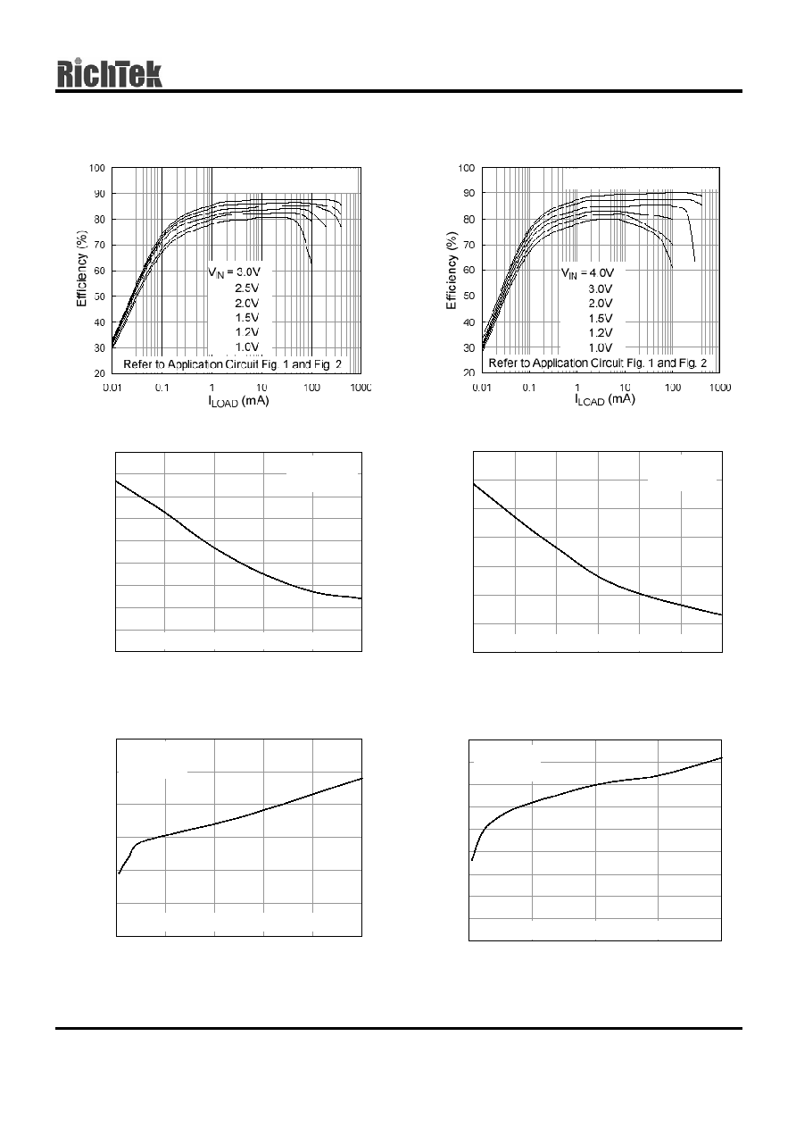
Typical Operating Charateristics
No Load Current
0
10
20
30
40
50
60
70
80
90
1
1.2
1.5
2
2.5
3
Input Voltage (V)
I
DD
(
A
)
Refer to Application Circuit Fig.1 and Fig.2
T
A
= 25
∞C
V
OUT
= 3.3V
µ
No Load Current
0
20
40
60
80
100
120
140
1
1.2
1.5
2
2.5
3
4
Input Voltage (V)
I
DD
(
A
)
Refer to Application Circuit Fig.1 and Fig.2
T
A
= 25
∞C
V
OUT
= 5.0V
µ
Start Up Voltage
0.8
0.9
1.0
1.1
1.2
1.3
1.4
0
20
40
60
80
100
I
LOAD
(mA)
I
nput
V
o
l
t
a
g
e
(
V
)
Refer to Application Circuit Fig.1 and Fig.2
T
A
= 25
∞C
V
OUT
= 3.3V
I
LOAD
(mA) in constant resistance load
Start Up Voltage
0.80
0.85
0.90
0.95
1.00
1.05
1.10
1.15
1.20
1.25
0
25
50
75
100
I
LOAD
(mA)
I
nput
V
o
l
t
a
g
e
(
V
)
Refer to Application Circuit Fig.1 and Fig.2
T
A
= 25
∞C
V
OUT
= 5.0V
I
LOAD
(mA) in constant resistance load
Efficiency
V
OUT
= 3.3V ; T
A
= 25∞C
Efficiency
V
OUT
= 5.0V ; T
A
= 25∞C

RT9262/A
Preliminary
www.richtek.com
DS9262/A-05 October 2002
8
Application Note
Output Voltage Setting
Referring to application circuits Fig.1 to Fig.5, the
output voltage of the switching regulator (V
OUT1
) can
be set with Eq.1.
The LDO output voltage (V
OUT2
of RT9262) can be
set with Eq.2.
And trip point of the low battery detector is 0.86V at
LBI pin of RT9262A.
Feedback Loop Design
Referring to application circuits Fig.1 to Fig.5, The
selection of R1, R2, R3, and R4 based on the trade-
off between quiescent current consumption and
interference immunity is stated below:
∑ Follow Eq.1 and Eq.2.
∑ Higher R reduces the quiescent current (Path
current = 1.25V/R2, and 0.86V/R3), however
resistors beyond 5M
are not recommended.
∑ Lower R gives better noise immunity, and is less
sensitive to interference, layout parasitics, FB/LFB
node leakage, and improper probing to FB/LFB
pins.
∑ A proper value of feed forward capacitor parallel
with R1 (or R4) on Fig.1 to Fig.5 can improve the
noise immunity of the feedback loops, especially in
an improper layout. An empirical suggestion is
around 100pF ~ 1nF for feedback resistors of M
,
and 10nF ~ 0.1
µF for feedback resistors of tens to
hundreds K
.
For applications without standby or suspend modes,
lower values of R1 to R4 are preferred. For
applications concerning the current consumption in
standby or suspend modes, the higher values of R1
to R4 are needed. Such "high impedance feedback
loops" are sensitive to any interference, which require
careful layout and avoid any interference, e.g.
probing to FB/LFB pins.
PRECAUTION 1: Improper probing to FB or LFB pin
will cause fluctuation at V
OUT1
and V
OUT2
. It may
damage RT9262/A and system chips because V
OUT1
may drastically rise to an over-rated level due to
unexpected interference or parasitics being added to
FB pin.
PRECAUTION 2: Disconnecting R1 or short circuit
across R2 may also cause similar IC damage as
described in precaution 1.
PRECAUTION 3: When large R values were used in
feedback loops, any leakage in FB/LFB node may
also cause V
OUT1
and V
OUT2
voltage fluctuation, and
IC damage. To be especially highlight here is when
the air moisture frozen and re-melt on the circuit
board may cause several
µA leakage between IC or
component pins. So, when large R values are used in
feedback loops, post coating, or some other
moisture-preventing processes are recommended.
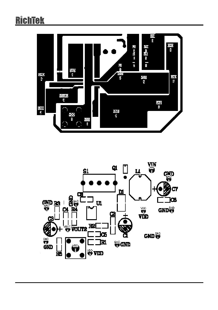
Layout Guide
∑ A full GND plane without gap break.
∑ V
OUT1
to GND noise bypass ≠ Short and wide
connection for C2 to Pin1 and Pin6.
∑ V
IN
to GND noise bypass ≠ Add a 100
µF
capacitor close to L1 inductor, when VIN is not an
idea voltage source.
∑ Minimized FB/LFB node copper area and keep
far away from noise sources.
∑ Minimized parasitic capacitance connecting to LX
and EXT nodes, which may cause additional
switching loss.
∑ The following diagram is an example of 2-layer
board layout for application circuits Fig.1 to Fig.4.
V
25
.
1
)
2
R
1
R
1
(
V
1
OUT
◊
+
=
Eq.1
V
86
.
0
)
3
R
4
R
1
(
V
2
OUT
◊
+
=
Eq.2
Prober Parasitics
FB Pin
R1
R2
V
OUT1
_
Q
+
Preliminary
RT9262/A
DS9262/A-05 October 2002
www.richtek.com
9
First Layer
Second Layer (Full GND Plane)
RT9262/A

RT9262/A
Preliminary
www.richtek.com
DS9262/A-05 October 2002
10
Package Information
Dimensions In Millimeters
Dimensions In Inches
Symbol
Min Max Min Max
A
4.801
5.004
0.189
0.197
B
3.810
3.988
0.150
0.157
C
1.346
1.753
0.053
0.069
D
0.330
0.508
0.013
0.020
F
1.194
1.346
0.047
0.053
H
0.178
0.254
0.007
0.010
I
0.102
0.254
0.004
0.010
J
5.791
6.198
0.228
0.244
M
0.406
1.270
0.016
0.050
8≠Lead SOP Plastic Package
F
A
J B
D
I
C
M
H

Preliminary
RT9262/A
DS9262/A-05 October 2002
www.richtek.com
11

RT9262/A
Preliminary
www.richtek.com
DS9262/A-05 October 2002
12
RICHTEK TECHNOLOGY CORP.
Headquarter
5F, No. 20, Taiyuen Street, Chupei City
Hsinchu, Taiwan, R.O.C.
Tel: (8863)5526789 Fax: (8863)5526611
RICHTEK TECHNOLOGY CORP.
Taipei Office (Marketing)
8F-1, No. 137, Lane 235, Paochiao Road, Hsintien City
Taipei County, Taiwan, R.O.C.
Tel: (8862)89191466 Fax: (8862)89191465
Email: marketing@richtek.com