Preliminary
RT9808
DS9808-01 January 2002
www.richtek.com
1
Micro-Power Voltage Detectors
General Description
The RT9808 is a micro-power voltage detector
supervising the power supply voltage level for
microprocessors (
µ
P) or digital systems. It provides
internally fixed threshold levels with 0.1V per step
ranging from 1.5V to 5V, which covers most digital
applications. It features low supply current of 3
µ
A.
The RT9808 performs supervisory function by
sending out a reset signal whenever the VDD voltage
falls below a preset threshold level. This reset signal
will last the whole period before VDD recovering.
Once VDD recovered up-crossing the threshold level,
the reset signal will be released if VDD is above
threshold and last for the whole period of reset active
time out.
RT9808 is n-channel, open-drain output.
Applications
Computers
Controllers
Intelligent Instruments
Critical
µ
P and
µ
C Power Monitoring
Portable/Battery-Powered Equipment
Ordering Information
RT9808-
Features
Internally Fixed Threshold 1.5V to 5V in 0.1V Step
±
2% Accuracy
Low Supply Current 3
µ
A
Quick Reset within 20
µ
S
Built-in Recovery Delay 200mS
Low Functional Supply Voltage 0.9V
N-Channel Open Drain Output
Small 3-Pin SOT-23/SOT89 and 5-Pin SOT-25
Packages
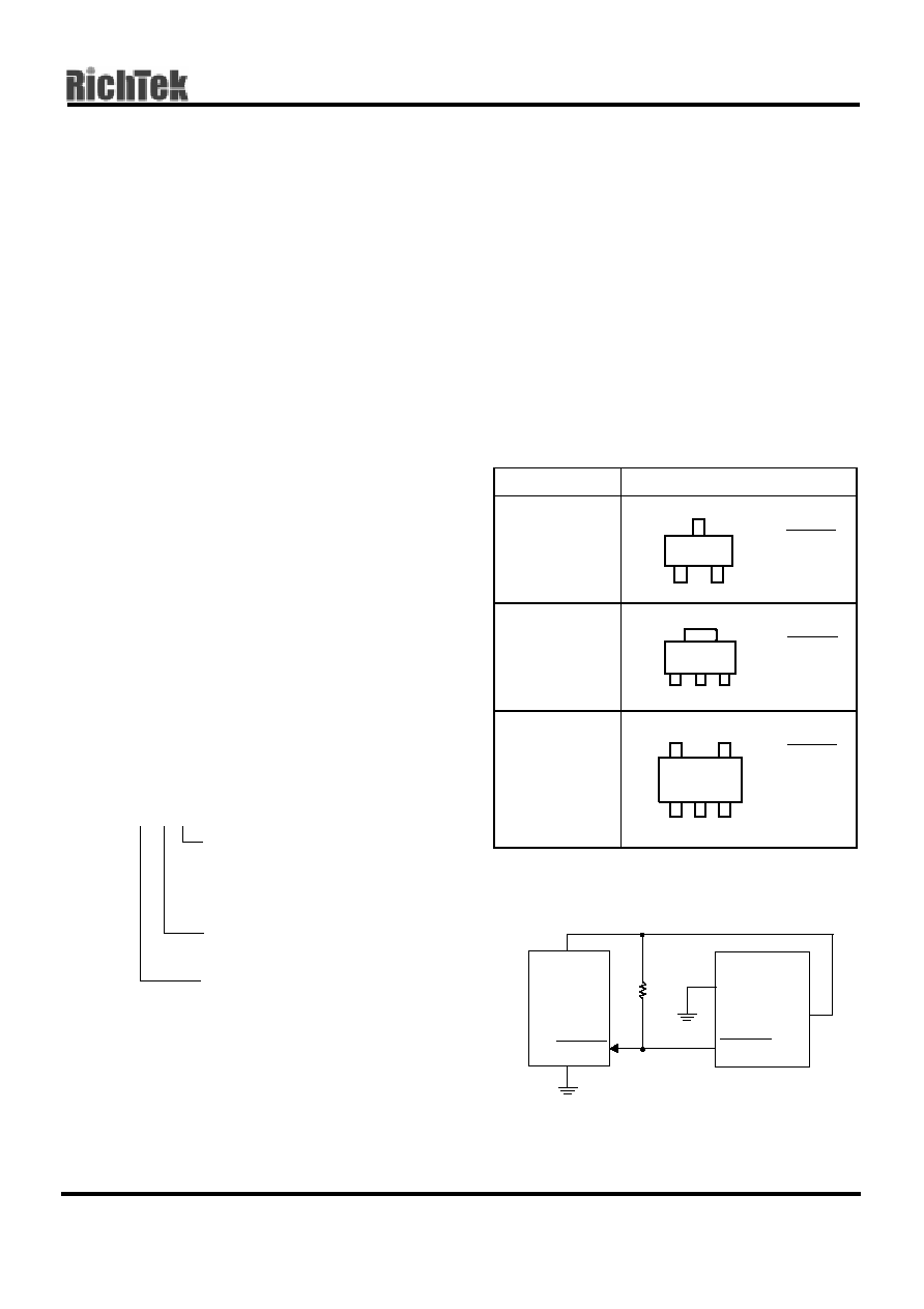
Pin Configurations
Part Number
Pin Configurations
RT9808-
CV
(Plastic SOT-23)
TOP VIEW
1. RESET
2. GND
3. VDD
RT9808-
CX
(Plastic SOT-89)
TOP VIEW
1. RESET
2. VDD
3. GND
RT9808-
CB
(Plastic SOT-25)
TOP VIEW
1. RESET
2. VDD
3. GND
4. NC
5. NC
Typical Application Circuit
Operating temperature range
C: Commercial standard
Package Type
V : SOT-23
X : SOT-89
B : SOT-25
Reset Threshold
15 : 1.5V
16 : 1.6V
:
49 : 4.9V
50 : 5.0V
VDD
µ
P
RESET
RT9808
VDD
RESET
GND
Pull
Up
100K
1
3
2
1
2
3
5
4
3
2
1
RT9808
Preliminary
www.richtek.com
DS9808-01 January 2002
2
Pin Description
Pin Name
Pin Function
GND
Ground Pin
RESET
Reset Pulse Output, Negative Pulse
VDD
Power Pin
NC
No Connected
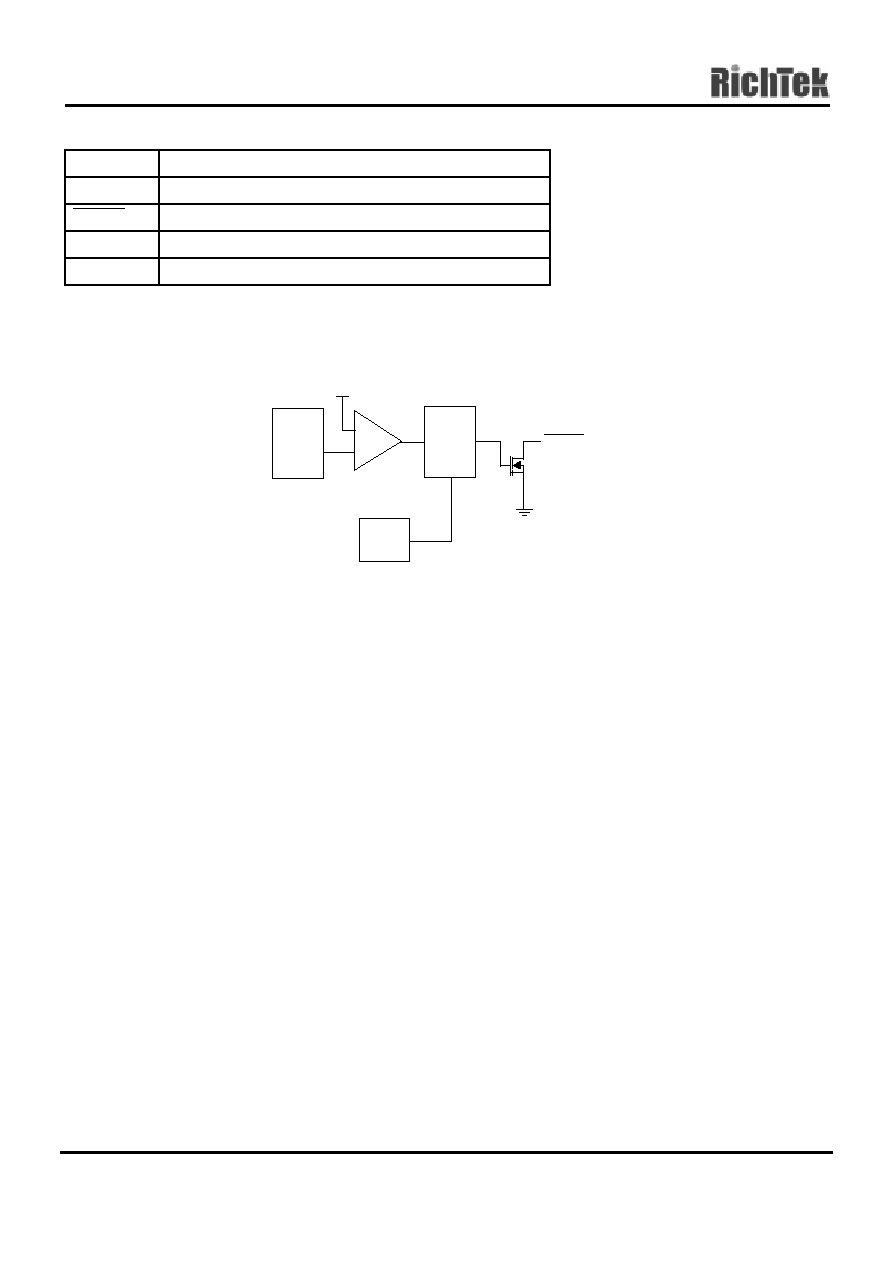
Function Block Diagram
VSET
CMP
TIMER
VDD
POR
RESET
N
Threshold Voltage Setting
Power On Reset
Preliminary
RT9808
DS9808-01 January 2002
www.richtek.com
3
Absolute Maximum Ratings
Terminal Voltage (with Respect to GND)
VDD
-0.3V to 6.0V
All Other Inputs
-0.3V to VDD+0.3V
Input Current, VDD
20mA
Output Current, RESET
20mA
Power Dissipation, P
D
@ T
A
= 25
∞
C
SOT-23
0.25W
SOT-89
0.5W
SOT-25
0.25W
Operating Junction Temperature Range
-40
∞
C ~ 125
∞
C
Storage Temperature Range
-65
∞
C ~ 125
∞
C
Package Thermal Resistance
SOT-23,
JA
250
∞
C /W
SOT-89,
JC
100
∞
C /W
SOT-89,
JA
300
∞
C /W
SOT-25,
JA
250
∞
C /W
Lead Temperature (Soldering, 5sec.)
260
∞
C
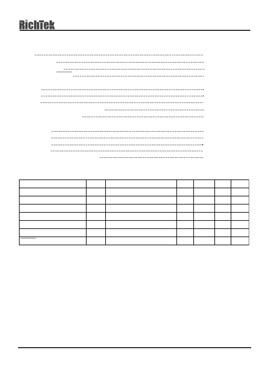
Electrical Characteristics
(VDD
= 3.0, unless specified)
Note1: 1.5V ~ 5V, step 0.1V
Parameter
Symbol
Test Conditions
Min
Typ
Max
Units
Operating VDD (V
OUT
) Range
V
DD
0.9
--
6
V
Supply Current
I
DD
V
DD
= 1.5V ~ 5V, I
OUT
= 0
--
3
--
µ
A
Reset Threshold
V
TH
T
A
= 27
∞
C
--
Note1
--
V
Threshold Voltage Accuracy
V
TH
T
A
= 27
∞
C
--
--
2
%
V
CC
Drop to Reset Delay
t
RD
Drop = -125mV
--
--
20
µ
S
Reset Active Time Out Period
t
RP
V
DD
1.02
◊
V
TH
--
200
--
mS
RESET Output Voltage
V
OL
V
DD
< V
TH
, I
SINK
> 3.5mA
--
0.4
--
V
RT9808
Preliminary
www.richtek.com
DS9808-01 January 2002
4
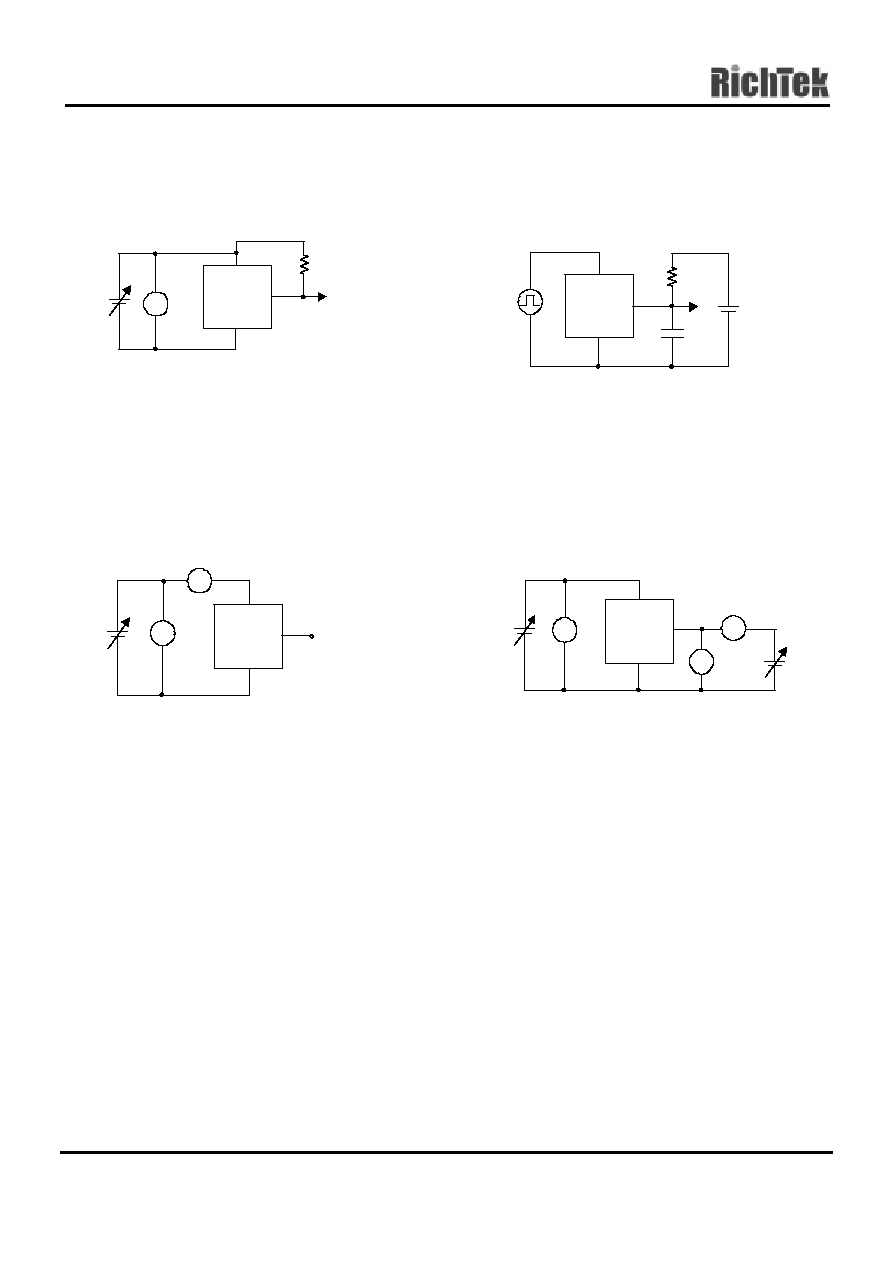
Measuring Circuit
(1) Detection Voltage
(2) Current Consumption
(3) Output Transistor Current
(4) Dynamic Response
RT9808
V
R (100k
)
Oscilloscope
V
SS
V
DD
V
DD
OUT
RT9808
V
A
V
SS
V
DD
V
DD
OUT
V
A
RT9808
V
SS
V
DD
V
DD
OUT
V
V
DS
RT9808
V
SS
V
DD
OUT
P.G
CL
CRT
6V
100k

Preliminary
RT9808
DS9808-01 January 2002
www.richtek.com
5
Typical Operating Characteristics
Nch Driver Output Current vs. V
DS
0
1
2
3
4
5
6
7
0
0.5
1
1.5
2
2.5
3
V
DS
(V)
O
u
t
put
C
u
r
r
e
nt
I
OU
T
(m
A
)
1.7V
1.5V
T
A
= 25
∞
C
RT9808-20CV
Nch Driver Output Current vs. V
DS
0
2
4
6
8
10
12
0
0.5
1
1.5
2
2.5
3
V
DS
(V)
O
u
t
put
C
u
r
r
e
nt
I
OU
T
(m
A
)
2.2V
2.0V
1.5V
T
A
= 25
∞
C
RT9808-24CV
Nch Driver Output Current vs. V
DS
0
3
6
9
12
15
18
0
0.5
1
1.5
2
2.5
3
V
DS
(V)
O
u
t
put
C
u
r
r
e
nt
I
OUT
(m
A
)
1.5V
2.0V
2.8V
T
A
= 25
∞
C
RT9808-30CV
Nch Driver Output Current vs. V
DS
0
6
12
18
24
30
36
0
1
2
3
4
V
DS
(V)
O
u
t
put
C
u
r
r
e
nt
I
OUT
(m
A
)
2.0V
2.5V
4.0V
3.5V
3.0V
1.5V
T
A
= 25
∞
C
RT9808-45CV
Nch Driver output Current vs. V
DS
0
8
16
24
32
40
0
1
2
3
4
5
V
DS
(V)
O
u
t
put
C
u
r
r
e
nt
I
OUT
(m
A
)
2.0V
2.5V
4.0V
3.5V
3.0V
1.5V
4.5V
T
A
= 25
∞
C
RT9808-50CV
Output Voltage vs. Input Voltage
0
1
2
3
4
5
6
7
0.0
1.0
2.0
3.0
4.0
5.0
6.0
Input Voltage V
IN
(V)
O
u
t
put
V
o
l
t
a
g
e
V
OU
T
(V
)
2.0V
2.4V
4.5V
3.0V
5.0V
T
A
= 25
∞
C
RT9808
Preliminary
www.richtek.com
DS9808-01 January 2002
6
Supply Current vs. Input Voltage
0
1
2
3
4
0
1
2
3
4
5
6
Input Voltage V
IN
(V)
S
uppl
y
C
u
r
r
e
nt
I
SS
(
A)
-30 C
25 C
80 C
RT9808-20CV
µ
∞
∞
∞
Supply Current vs. Input Voltage
0
1
2
3
4
0
1
2
3
4
5
6
Input Voltage V
IN
(V)
S
u
ppl
y
C
u
r
r
e
nt
I
SS
(
A
)
-30 C
25 C
80 C
RT9808-24CV
∞
µ
∞
∞
Supply Current vs. Input Voltage
0
1
2
3
4
0
1
2
3
4
5
6
Input Voltage V
IN
(V)
S
uppl
y
C
u
r
r
e
nt
I
SS
(
A)
-30 C
25 C
80 C
RT9808-30CV
∞
µ
∞
∞
Supply Current vs. Input Voltage
0
1
2
3
4
5
0
1
2
3
4
5
6
Input Voltage V
IN
(V)
S
uppl
y
C
u
r
r
e
nt
I
SS
(
A)
-30 C
25 C
80 C
RT9808-45CV
∞
µ
∞
∞
Supply Current vs. Input Voltage
0
1
2
3
4
5
0
1
2
3
4
5
6
Input Voltage V
IN
(V)
S
uppl
y
C
u
r
r
e
nt
I
SS
(
A)
-30 C
25 C
80 C
RT9808-50CV
∞
µ
∞
∞
Reset Threshold Deviation vs. Temp.
1.9
2.3
2.7
3.1
3.5
3.9
4.3
4.7
5.1
-40
-15
10
35
60
85
Temperture ( C)
T
h
res
h
o
l
d
(V
)
2V
2.4V
3V
4.5V
5V
∞

Preliminary
RT9808
DS9808-01 January 2002
www.richtek.com
7
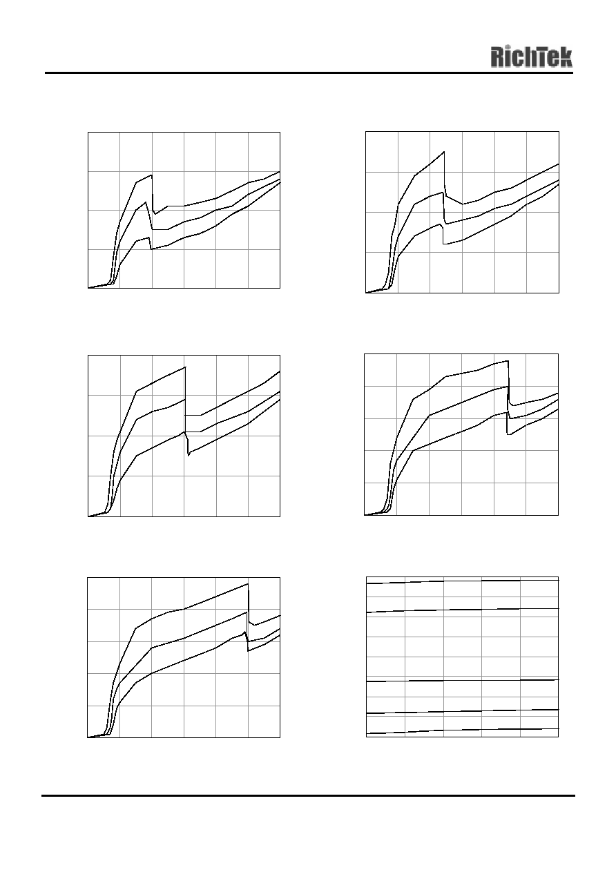
Nch Driver Output Current vs. Input Voltage
0
2
4
6
8
10
0
0.5
1
1.5
2
2.5
3
Input Voltage V
IN
(V)
O
u
t
put
C
u
r
r
e
nt
I
OUT
(m
A
)
-30 C
25 C
80 C
RT9808-20CV
V
DS
= 0.5V
∞
∞
∞
Nch Driver Output Current vs. Input Voltage
0
2
4
6
8
10
0
0.5
1
1.5
2
2.5
3
Input Voltage V
IN
(V)
O
u
t
put
C
u
r
r
e
nt
I
OUT
(m
A
)
-30 C
25 C
80 C
RT9808-24CV
V
DS
= 0.5V
∞
∞
∞
Nch Driver Output Current vs. Input Voltage
0
2
4
6
8
10
12
0
0.5
1
1.5
2
2.5
3
3.5
Input Voltage V
IN
(V)
O
u
t
put
C
u
r
r
e
nt
I
OUT
(m
A
)
-30 C
25 C
80 C
RT9808-30CV
V
DS
= 0.5V
∞
∞
∞
Nch Driver Output Current vs. Input Voltage
0
2
4
6
8
10
12
14
16
0
1
2
3
4
5
Input Voltage V
IN
(V)
O
u
t
put
C
u
r
r
e
nt
I
OUT
(m
A
)
-30 C
25 C
80 C
RT9808-45CV
V
DS
= 0.5V
∞
∞
∞
∞
Nch Driver Output Current vs. Input Voltage
0
3
6
9
12
15
18
0
1
2
3
4
5
6
Input Voltage V
IN
(V)
O
u
t
put
C
u
r
r
e
nt
I
OUT
(m
A
)
-30 C
25 C
80 C
RT9808-50CV
V
DS
= 0.5V
∞
∞
Power-Up reset Timeout vs. Temp.
50
100
150
200
250
300
350
-40
-15
10
35
60
85
Temperture ( C)
P
o
w
e
r-U
p
Res
e
t
T
i
m
e
o
u
t
(m
s
)
3V
4.5V
5V
2.4V
2V
∞
RT9808
Preliminary
www.richtek.com
DS9808-01 January 2002
8
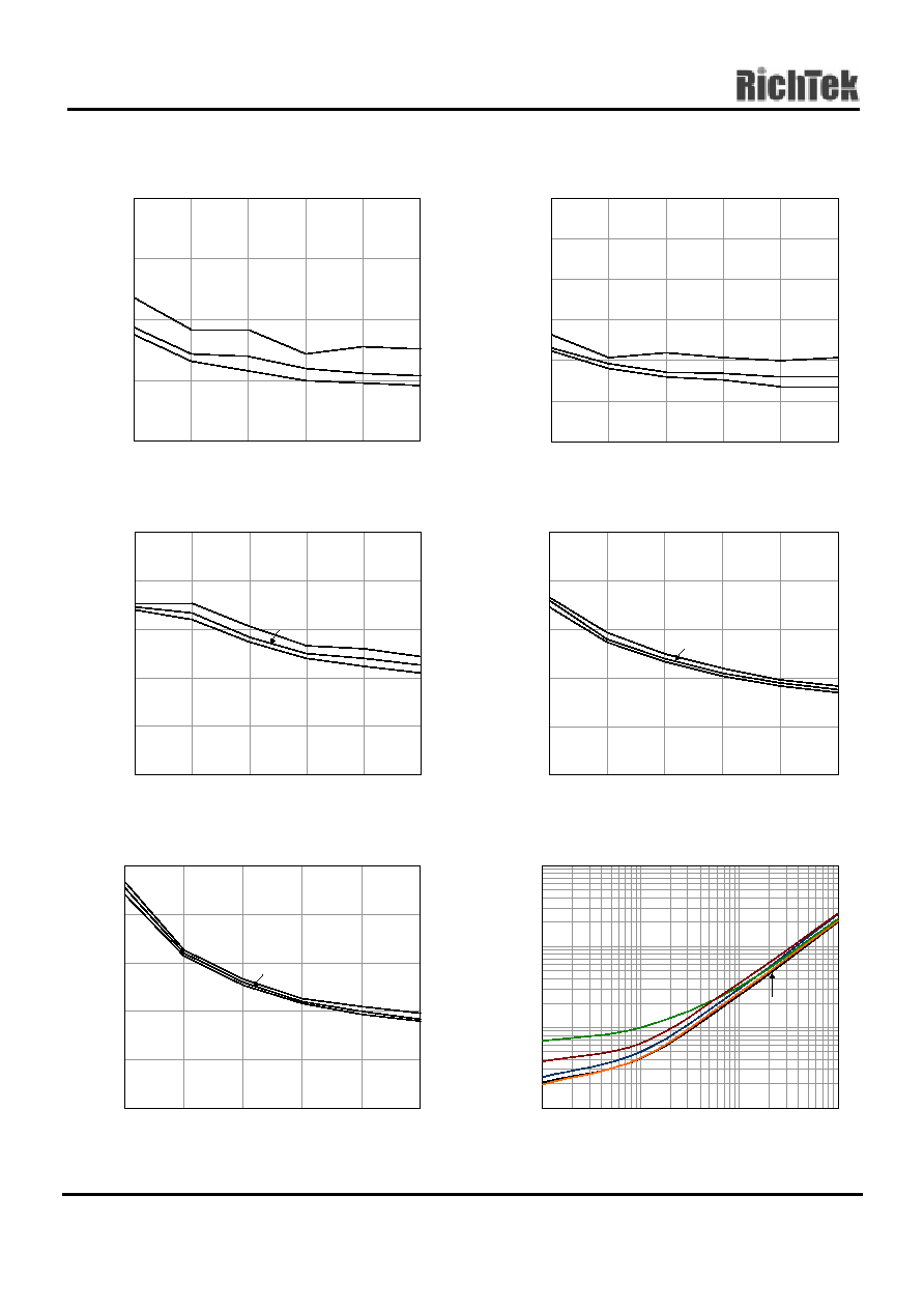
Power-Down Reset Delay vs. Temp.
0.0
0.3
0.6
0.9
1.2
1.5
-40
-15
10
35
60
85
Temperture ( C)
P
o
w
e
r-Dow
n
R
e
s
e
t
Del
a
y
( s
)
V
drop
= 150mV
RT9808-50CV
V
drop
= 200mV
V
drop
= 250mV
∞
µ
Power-Down Reset Delay vs. Temp.
0.0
0.3
0.6
0.9
1.2
1.5
-40
-15
10
35
60
85
Temperture ( C)
P
o
w
e
r-D
o
w
n
Res
e
t
D
e
l
a
y
( s
)
V
drop
= 150mV
RT9808-30CV
V
drop
= 200mV
V
drop
= 250mV
∞
µ
Power-Down Reset Delay vs. Temp.
0.0
0.3
0.6
0.9
1.2
1.5
-40
-15
10
35
60
85
Temperture ( C)
P
o
w
e
r-D
o
w
n
R
e
s
e
t
Del
a
y
( s
)
V
drop
= 150mV
RT9808-45CV
V
drop
= 200mV
V
drop
= 250mV
∞
µ
Power-Down Reset Delay vs. Temp.
0.0
1.0
2.0
3.0
4.0
-40
-15
10
35
60
85
Temperture ( C)
P
o
w
e
r-Dow
n
R
e
s
e
t
D
e
l
a
y
( s
)
V
drop
= 150mV
RT9808-20CV
V
drop
= 200mV
V
drop
= 250mV
∞
µ
Power-Down Reset Delay vs. Temp.
0.0
0.5
1.0
1.5
2.0
2.5
3.0
-40
-15
10
35
60
85
Temperture ( C)
P
o
w
e
r-Dow
n
R
e
s
e
t
Del
a
y
( s
)
V
drop
= 150mV
RT9808-24CV
V
drop
= 200mV
V
drop
= 250mV
∞
µ
Output Delay Time vs. Load Capacitance
1
10
100
1000
0.0001
0.001
0.01
0.1
Load Capacitance C
OUT
(uF)
O
u
t
put
D
e
l
a
y
T
i
m
e
t
P
(m
s
)
5V
4.5V
3V
2V
2.4V
T
A
= 25
∞
C

Preliminary
RT9808
DS9808-01 January 2002
www.richtek.com
9
Package Information
Dimensions In Millimeters
Dimensions In Inches
Symbol
Min
Max
Min
Max
A
0.889
1.295
0.035
0.051
A1
--
0.152
--
0.006
B
1.397
1.803
0.055
0.071
b
0.356
0.508
0.014
0.020
C
2.591
2.997
0.102
0.118
D
2.692
3.099
0.106
0.122
e
1.803
2.007
0.071
0.079
H
0.102
0.254
0.004
0.010
L
0.356
0.610
0.014
0.024
SOT-23 Plastic Surface Mount
L
H
b
A
A1
D
e
B
C
RT9808
Preliminary
www.richtek.com
DS9808-01 January 2002
10
Dimensions In Millimeters
Dimensions In Inches
Symbol
Min
Max
Min
Max
A
1.397
1.600
0.055
0.063
b
0.356
0.483
0.014
0.019
B
2.388
2.591
0.094
0.102
b1
0.406
0.533
0.016
0.021
C
--
4.242
--
0.167
C1
0.787
1.194
0.031
0.047
D
4.394
4.597
0.173
0.181
D1
1.397
1.753
0.055
0.069
e
1.448
1.549
0.057
0.061
H
0.381
0.432
0.015
0.017
3-Lead SOT-89 Surface Mount
D
D1
C
C1
B
e
e
A
b
b1
b
A
H
Preliminary
RT9808
DS9808-01 January 2002
www.richtek.com
11
Dimensions In Millimeters
Dimensions In Inches
Symbol
Min
Max
Min
Max
A
0.889
1.295
0.035
0.051
A1
0.000
0.152
0.000
0.006
B
1.397
1.803
0.055
0.071
b
0.356
0.559
0.014
0.022
C
2.591
2.997
0.102
0.118
D
2.692
3.099
0.106
0.122
e
0.838
1.041
0.033
0.041
H
0.102
0.254
0.004
0.010
L
0.356
0.610
0.014
0.024
SOT- 25 Surface Mount Package
b
B
C
D
L
H
A1
e
A

RT9808
Preliminary
www.richtek.com
DS9808-01 January 2002
12
RICHTEK TECHNOLOGY CORP.
Headquarter
5F, No. 20, Taiyuen Street, Chupei City
Hsinchu, Taiwan, R.O.C.
Tel: (8863)5526789 Fax: (8863)5526611
RICHTEK TECHNOLOGY CORP.
Taipei Office (Marketing)
8F-1, No. 137, Lane 235, Paochiao Road, Hsintien City
Taipei County, Taiwan, R.O.C.
Tel: (8862)89191466 Fax: (8862)89191465
Email: marketing@richtek.com