
'2003.10.3
LOW NOISE 150mA WL-CSP LDO
R1115Z SERIES
Rev. 1.10
- 1 -
�
�
�
�OUTLINE
The R1115Z Series are CMOS-based voltage regulator ICs with extremely low supply current, low ON-resistance, and high
ripple rejection. Each of these ICs consists of a voltage reference unit, an error amplifier, resistor-net for voltage setting, a
current limit circuit, and a chip-enable circuit.
These ICs perform with low dropout voltage and a chip-enable function. The line transient response and load transient
response of the R1115Z Series are excellent, thus these ICs are very suitable for the power supply for hand-held
communication equipment.
The output voltage of these ICs is fixed with high accuracy. Since the package for these ICs is WL-CSP-4P4, therefore high
density mounting of the ICs on boards is possible.
�
�
�
�FEATURES
z Low Supply Current .................................................. Typ. 75
µ
A
z Standby Mode............................................................ Typ. 0.1
µ
A
z Low Dropout Voltage ................................................ Typ. 0.22V (I
OUT
=150mA 3.0V Output type)
z High Ripple Rejection............................................... Typ. 70dB (f=1kHz 3.0V Output type) / 60dB (f=10kHz)
z Low Temperature-Drift Coefficient of Output Voltage Typ. ±100ppm/
∞
C
z Excellent Line Regulation ......................................... Typ. 0.02%/V
z High Output Voltage Accuracy.................................. ±2.0%
z Small Package ..........................................................WL-CSP-4P4
z Output Voltage...........................................................Stepwise setting with a step of 0.1V in the range of 1.5V to 4.0V is
possible
z Built-in Fold Back Protection Circuit........................Typ. 40mA (Current at short mode)
z Ceramic capacitors are recommended to be used with this IC
C
IN
=C
OUT
=1
µ
F(V
OUT
<2.5V)
...........................................................................................
C
IN
=1
µ
F, C
OUT
=0.47
µ
F (V
OUT
2.5V)
�
�
�
�APPLICATIONS
z Power source for portable communication equipment.
z Power source for electrical appliances such as cameras, VCRs and camcorders.
z Power source for battery-powered equipment.

Rev. 1.10
- 2 -
�
�
�
�BLOCK DIAGRAMS
R1115ZXX1A R1115ZXX1B
V
DD
V
OUT
GND
Vref
+
-
CE
Current Limit
V
DD
V
OUT
GND
Vref
+
-
CE
Current Limit
R1115ZXX1D
Vref
Current Limit
+
-
V
OUT
GND
CE
V
DD
�
�
�
�SELECTION GUIDE
The output voltage, version, and the taping type for the ICs can be selected at the user's request. The selection can be made
with designating the part number as shown below;
R1115ZXX1X-XX
Part Number
a b c d
Code Contents
a
Designation of Package Type:
Z: WL-CSP-4P4
b
Setting Output Voltage (V
OUT
):
Stepwise setting with a step of 0.1V in the range of 1.5V to 4.0V is possible.
c
Designation of Active Type:
A: active low type
B: active high type
D: active high, with auto discharge
d
Designation of Taping Type:
Ex. TR (refer to Taping Specifications; TR type is the standard direction.)

Rev. 1.10
- 3 -
�
�
�
�PIN CONFIGURATION
�
�
�
�PIN DESCRIPTIONS
R1115Z
Pin No.
Symbol
Description
1
V
DD
Input Pin
2
CE
Chip Enable Pin
3
GND
Ground Pin
4
V
OUT
Output pin
�
�
�
�ABSOLUTE MAXIMUM RATINGS
Item Symbol
Rating
Unit
Input Voltage
V
IN
6.5 V
Input Voltage( CE or CE Pin)
V
CE
-0.3
~
V
IN
+0.3 V
Output Voltage
V
OUT
-0.3
~
V
IN
+0.3 V
Output Current
I
OUT
200 mA
Power Dissipation
P
D
*Note
mW
Operating Temperature Range
Topt
-40 ~ 85
∞
C
Storage Temperature Range
Tstg
-55 ~ 125
∞
C
*Note: Refer to the page on Power Dissipation.
Bump side
Silicon Side
4 V
OUT
3 GND
2 CE
1 V
DD
3
4
1
2

Rev. 1.10
- 4 -
s
POWER DISSIPATION
*Measurement Conditions
Test Condition: Mounted on PCB (Wind velocity=0m/s)
Board Material: FR-4 (Double layer)
Board Size: 40mm
◊
40mm
◊
t1.6mm
Metal Ratio: 50%
*Result
P
D
=600mW, Thermal Resistance 167
∞
C/W
0
100
200
300
400
500
600
700
0
25
50
75
100
125
Temperature Topt
Po
we
r Di
ssi
p
a
t
i
o
n
(
m
W
)
(
∞
C)
Rev. 1.10
- 5 -
�
�
�
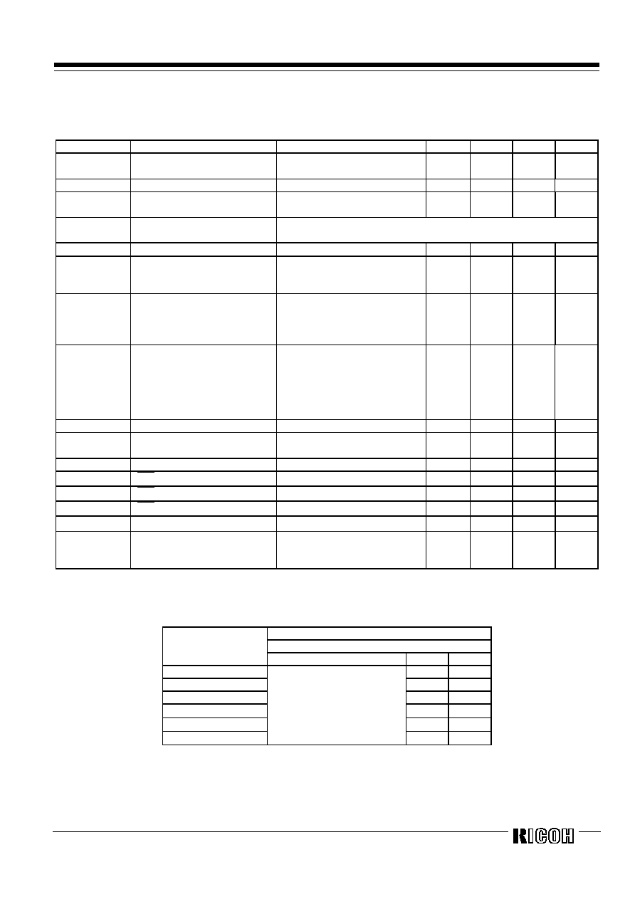
�ELECTRICAL CHARACTERISTICS
R1115ZXX1X
Topt=25
∞
C
Symbol Item
Conditions
Min.
Typ.
Max.
Unit
V
OUT
Output
Voltage
V
IN
= Set V
OUT
+1V
1mA
I
OUT
30mA
V
OUT
◊
0.980
V
OUT
◊
1.020
V
I
OUT
Output
Current
V
IN
- V
OUT
= 1.0V
150
mA
V
OUT
/
I
OUT
Load Regulation
V
IN
= Set V
OUT
+1V
1mA
I
OUT
150mA
22
40
mV
V
DIF
Dropout
Voltage
Refer to the ELECTRICAL CHARACTERISTICS by OUTPUT
VOLTAGE
I
SS
Supply
Current
V
IN
= Set V
OUT
+1V, I
OUT
=0mA
75
95
µ
A
Istandby Supply
Current
(Standby)
V
IN
= Set V
OUT
+1V
V
CE
= GND(B/D version)
= V
DD
(A version)
0.1
1.0
µ
A
V
OUT
/
V
IN
Line Regulation
V
OUT
>1.7V,
Set V
OUT
+0.5V
V
IN
6.0V
(V
OUT
1.7V, 2.2V
V
IN
6.0V) I
OUT
= 30mA
0.02
0.10
%/V
RR Ripple
Rejection
f=1kHz
f=10kHz
Ripple 0.5Vp-p
V
OUT
>1.7V, V
IN
-V
OUT
=1.0V
V
OUT
1.7,V
IN
-V
OUT
=1.2V
I
OUT
=30mA
70
60
dB
V
IN
Input
Voltage
2.0 6.0 V
V
OUT
/
T
Output Voltage
Temperature Coefficient
I
OUT
= 30mA
-40
∞
C
Topt
85
∞
C
±100
ppm
/
∞
C
Ilim Short
Current
Limit
V
OUT
= 0V
40
mA
R
PU
CE Pull-up Resistance
0.7
2.0
8.0
M
V
CEH
CE Input Voltage "H"
1.5
V
IN
V
V
CEL
CE Input Voltage "L"
0.0
0.3
V
e
n
Output Noise
BW=10Hz to 100kHz
30
µ
Vrms
R
LOW
On Resistance of Nch for
auto-discharge (Only for D
version)
V
CE
=0V
60
ELECTRICAL CHARACTERISTICS by OUTPUT VOLTAGE
Topt = 25
∞
C
Dropout Voltage
V
DIF
(V)
Output Voltage
V
OUT
(V)
Condition Typ.
Max.
V
OUT
= 1.5
0.38 0.70
V
OUT
= 1.6
0.36 0.65
V
OUT
= 1.7
0.34 0.60
1.8
V
OUT
2.0
0.32 0.55
2.1
V
OUT
2.7
0.28 0.50
2.8
V
OUT
4.0
I
OUT
= 150mA
0.22 0.35