
2000. 3.13
LOW NOISE 150mA LDO REGULATOR
R1122N SERIES
Rev. 1.10
- 1 -
n
OUTLINE
The R1122N Series are voltage regulator ICs with high output voltage accuracy, extremely low supply current, low ON-
resistance and high ripple rejection by CMOS process. Each of these voltage regulator ICs consists of a voltage reference unit,
an error amplifier, resistors, a current limit circuit, and a chip enable circuit. These ICs perform with low dropout voltage and
a chip enable function.
The line transient response and load transient response of the R1122N Series are excellent, thus these ICs are very suitable for
the power supply for hand-held communication equipment. The output voltage of these ICs is fixed with high accuracy.
Since the package for these ICs are SOT-23-5 (Mini-mold) package, high density mounting of the ICs on boards is possible.
n
FEATURES
l
Ultra-Low Supply Current.................................................TYP. 100
mA
l
Standby Mode ...................................................................TYP. 0.1
mA
l
Low Dropout Voltage ........................................................TYP. 0.19V (I
OUT
= 100mA, 3V Output type)
l
High Ripple Rejection .......................................................TYP. 80dB (f = 1kHz)
l
Low Temperature-Drift Coefficient of Output Voltage .....TYP.
�100ppm/�C
l
Excellent Line Regulation .................................................TYP. 0.05%/V
l
High Accuracy Output Voltage..........................................
�2.0%
l
Small Package ..................................................................SOT-23-5 (Mini-mold)
l
Output Voltage ..................................................................Stepwise setting with a step of 0.1V in the range of 1.5V to 5.0V
is possible.
l
Built-in chip enable circuit (2 Types; A: active "L", B: active "H")
l
Built-in Fold-back protection circuit .................................Short Current Typ. 30mA
l
Pinout ................................................................................Similar to the TK112, TK111
l
Ceramic Capacitors are Recommendable to be used with this IC.
n
APPLICATIONS
l
Power source for cellular phones such as GSM, CDMA, PCS and so forth.
l
Power source for domestic appliances such as cameras, VCRs and camcorders.
l
Power source for battery-powered equipment.

Rev. 1.10
- 2 -
n
BLOCK DIAGRAM
R1122NXX1A
R1122NXX1B
Vref
Current Limit
V
DD
3
1
2
4
V
OUT
GND
CE
Vref
Current Limit
V
DD
3
1
2
4
V
OUT
GND
CE
n
SELECTION GUIDE
The output voltage, the active type, the packing type, and the taping type for the ICs can be selected at the user's request.
The selection can be made by designating the part number as shown below :
R1122NXX1X-XX
�Part Number
- - -
a b
c
Code
Contents
a
Setting Output Voltage (V
OUT
) :
Stepwise setting with a step of 0.1V in the range of 1.5V to 5.0V is possible.
b
Designation of Active Type :
A : active "L" type
B : active "H" type
c
Designation of Taping Type :
Ex. TR, TL (refer to Taping Specifications; TR type is the standard direction.)
Rev. 1.10
- 3 -
n
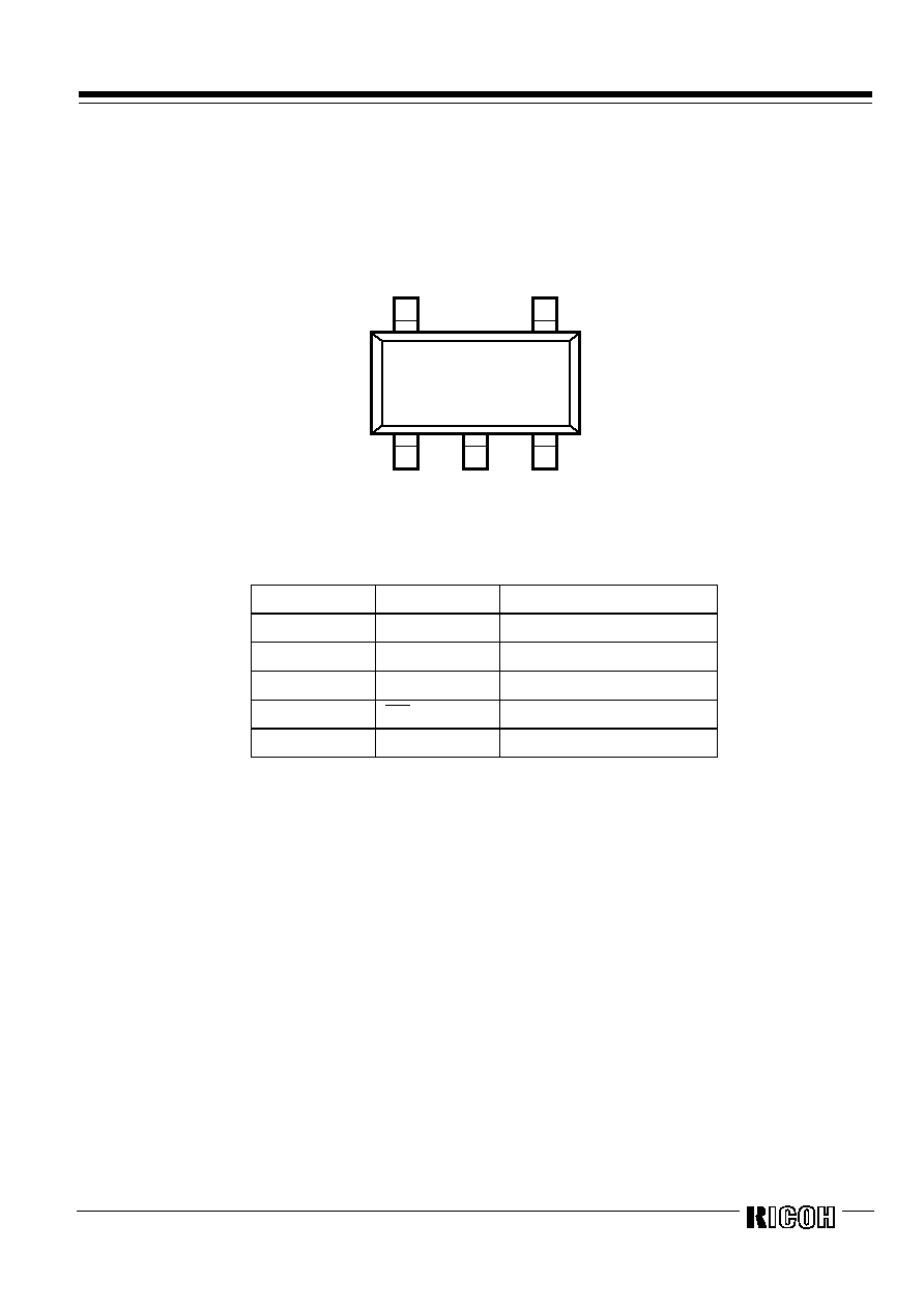
PIN CONFIGURATION
SOT-23-5
5
4
NC
CE
(mark side)
1
2
3
V
OUT
GND
V
DD
n
PIN DESCRIPTION
Pin No.
Symbol
Description
1
V
OUT
Output pin
2
GND
Ground Pin
3
V
DD
Input Pin
4
CE or CE
Chip Enable Pin
5
NC
No Connection

Rev. 1.10
- 4 -
n
ABSOLUTE MAXIMUM RATINGS
Symbol
Item
Rating
Unit
V
IN
Input Voltage
7.0
V
V
CE
Input Voltage (CE or CE Pin)
-0.3 ~ V
IN
+0.3
V
V
OUT
Output Voltage
-0.3~ V
IN
+0.3
V
I
OUT
Output Current
200
mA
P
D
Power Dissipation
250
mW
Topt
Operating Temperature
Range
-40 ~ 85
�C
Tstg
Storage Temperature Range
-55 ~ 125
�C
n
ELECTRICAL CHARACTERISTICS
l
R1122NXX1A
Topt = 25
�C
Symbol
Item
Conditions
MIN.
TYP.
MAX.
Unit
V
OUT
Output Voltage
V
IN
= Set V
OUT
+1V
1mA
� I
OUT
� 30mA
V
OUT
�0.98
V
OUT
�1.02
V
I
OUT
Output Current
V
IN
= Set V
OUT
+1V
When V
OUT
= Set V
OUT
-0.1V
150
mA
DV
OUT
/
DI
OUT
Load Regulation
V
IN
= Set V
OUT
+1V
1mA
� I
OUT
� 80mA
12
40
mV
V
DIF
Dropout Voltage
refer to the ELECTICAL CHARACTERISTICS by OUTPUT
VOLTAGE
I
SS
Supply Current
V
IN
= Set V
OUT
+1V
100
170
mA
Istandby
Supply Current (Standby)
V
IN
= V
CE
= Set V
OUT
+1V
0.1
1.0
mA
DV
OUT
/
DV
IN
Line Regulation
Set V
OUT
+0.5V
� V
IN
� 8V
I
OUT
= 30mA
0.05
0.20
%/V
RR
Ripple Rejection
f = 1KHz, Ripple 0.5Vp-p
V
IN
= Set V
OUT
+1V
80
dB
V
IN
Input Voltage
2.0
6.0
V
DV
OUT
/
DT
Output Voltage
Temperature Coefficient
I
OUT
= 30mA
-40
�C � Topt � 85�C
�100
ppm
/
�C
Ilim
Short Current Limit
V
OUT
= 0V
30
mA
R
PU
CE Pull-up Resistance
2.5
5
10
M
W
V
CEH
CE Input Voltage "H"
1.5
V
IN
V
V
CEL
CE Input Voltage "L"
0
0.25
V
en
Output Noise
BW = 10Hz ~ 100kHz
30
mVrms

Rev. 1.10
- 5 -
l
R1122NXX1B
Topt=25
�C
Symbol
Item
Conditions
MIN.
TYP.
MAX.
Unit
V
OUT
Output Voltage
V
IN
= Set V
OUT
+1V
1mA
� I
OUT
� 30mA
V
OUT
�0.98
V
OUT
�1.02
V
I
OUT
Output Current
V
IN
= Set V
OUT
+1V
When V
OUT
= Set V
OUT
-0.1V
150
mA
DV
OUT
/
DI
OUT
Load Regulation
V
IN
= Set V
OUT
+1V
1mA
� I
OUT
� 80mA
12
40
mV
V
DIF
Dropout Voltage
refer to the ELECTICAL CHARACTERISTICS by OUTPUT
VOLTAGE
I
SS
Supply Current
V
IN
= Set V
OUT
+1V
100
170
mA
Istandby
Supply Current (Standby)
V
IN
= Set V
OUT
+1V
V
CE
= GND
0.1
1.0
mA
DV
OUT
/
DV
IN
Line Regulation
Set V
OUT
+0.5V
� V
IN
� 8V
I
OUT
= 30mA
0.05
0.20
%/V
RR
Ripple Rejection
f = 1KHz, Ripple 0.5Vp-p
V
IN
= Set V
OUT
+1V
80
dB
V
IN
Input Voltage
2.0
6.0
V
DV
OUT
/
DT
Output Voltage
Temperature Coefficient
I
OUT
= 30mA
-40
�C � Topt � 85�C
�100
ppm
/
�C
Ilim
Short Current Limit
V
OUT
= 0V
30
mA
R
PD
CE Pull-down Resistance
2.5
5
10
M
W
V
CEH
CE Input Voltage "H"
1.5
V
IN
V
V
CEL
CE Input Voltage "L"
0
0.25
V
en
Output Noise
BW = 10Hz ~ 100kHz
30
mVrms
l
ELECTRICAL CHARACTERISTICS by OUTPUT VOLTAGE
Topt = 25
�C
Dropout Voltage
V
DIF
(V)
Output Voltage
V
OUT
(V)
Conditions
TYP.
MAX.
1.5
� V
OUT
� 1.6
0.32
0.55
1.7
� V
OUT
� 1.8
0.28
0.47
1.9
� V
OUT
� 2.3
0.25
0.35
2.4
� V
OUT
� 2.7
0.20
0.29
2.8
� V
OUT
� 5.0
I
OUT
= 100mA
0.19
0.26
Rev. 1.10
- 6 -
n
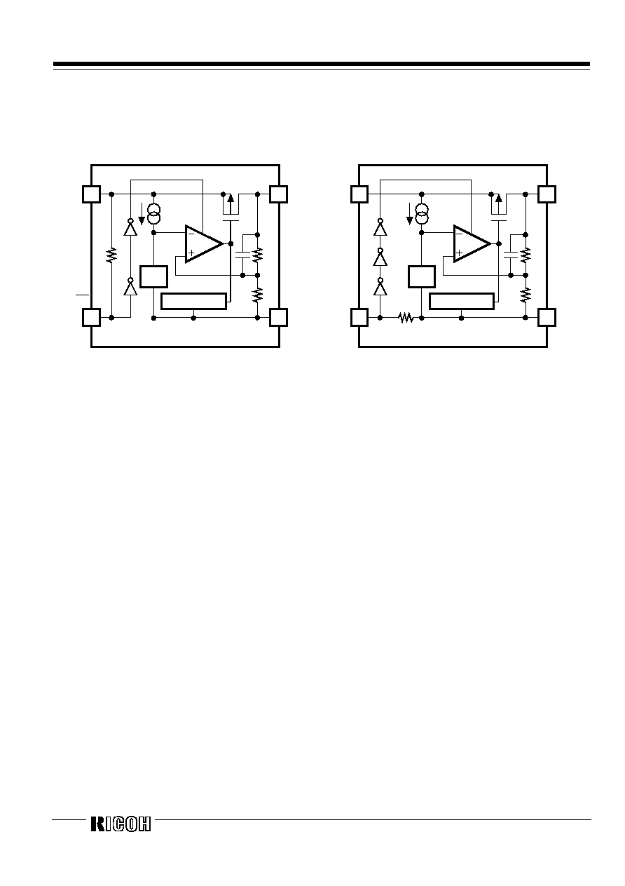
OPERATION
R1122XX1A
R1122XX1B
V
DD
3
1
2
4
V
OUT
GND
R2
R1
CE
Current Limit
Vref
V
DD
3
1
2
4
V
OUT
GND
R2
R1
CE
Current Limit
Vref
In these ICs, fluctuation of Output Voltage, V
OUT
is detected by Feed-back Registers, R1 and R2, and the result is compared
with a reference voltage by Error Amplifier, so that a constant voltage is output.
A current limit circuit for protection at short mode, and a chip enable circuit are included.

Rev. 1.10
- 7 -
n
TEST CIRCUITS
R1121Nxx1B Series
V
DD
1
3
2
4
V
OUT
I
OUT
IN
OUT
GND
CE
0.1
�
F
2.2
�
F
R1121Nxx1B Series
V
DD
1
3
2
4
V
OUT
I
SS
IN
OUT
GND
CE
0.1
�
F
2.2
�
F
Fig.1 Standard test Circuit
Fig.2 Supply Current Test Circuit
R1121Nxx1B Series
V
DD
1
3
P.G
2
4
V
OUT
I
OUT
IN
OUT
GND
CE
R1121Nxx1B Series
V
DD
1
3
2
4
V
OUT
IN
OUT
GND
I1
I2
CE
1
�
F
Fig.3 Ripple Rejection, Line Transient Response Test
Circuit
Fig.4 Load Transient Response Test Circuit
2.2
mF
2.2
mF
2.2
mF
R1122Nxx1B
Series
R1122Nxx1B
Series
R1122Nxx1B
Series
R1122Nxx1B
Series

Rev. 1.10
- 8 -
n
TECHNICAL NOTES
When using these ICs, consider the following points:
Phase Compensation
In these ICs, phase compensation is made for securing stable operation even if the load current is varied. For this purpose, be
sure to use a capacitor C
OUT
with good frequency characteristics and ESR (Equivalent Series Resistance).
(note: When the additional ceramic capacitors are connected to the Output Pin with Output capacitor for phase compensation,
the operation might be unstable. Because of this, test these ICs with as same external components as ones to be used on the
PCB.)
Recommended Capacitors; GRM40X5R225K6.3 (Murata)
GRM40-034X5R335K6.3 (Murata)
GRM40-034X5R475K6.3 (Murata)
PCB Layout
Make VDD and GND line sufficient. When the impedance of these is high, it would be a cause of picking up the noise or
unstable operation. Connect a capacitor with a capacitance of 2.2
mF or more between VDD and GND pin as close as possible.
Set external components, especially output capacitor as close as possible to the ICs and make wiring shortest.

Rev. 1.10
- 9 -
n
TYPICAL APPLICATION
R1111NXX1A V
OUT
OUT
IN
V
DD
GND
CE
Cap.
Cap.
R1111Nxx1B V
OUT
OUT
IN
V
DD
GND
CE
Cap.
Cap.
(External Components)
Output Capacitor; Ceramic 2.2
m
F(Set Output Voltage in the range from 2.5 to 5.0V)
Ceramic 4.7
m
F (Set Output Voltage in the range from 1.5 to 2.5V)
Input Capacitor; Ceramic 2.2
m
F
R1122Nxx1A
Series
R1122Nxx1B
Series
Rev. 1.10
- 10 -
n
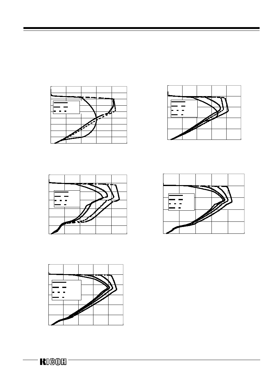
TYPICAL CHARACTERISTICS
1)
Output Voltage vs. Output Current
R11x2N151B
0
0.2
0.4
0.6
0.8
1
1.2
1.4
1.6
1.8
0
100
200
300
400
500
Output Current Iout[mA]
Output Voltage Vout[V]
VIN=2.0V
VIN=2.5V
VIN=3.5V
R11x2N201B
0
0.5
1
1.5
2
2.5
0
100
200
300
400
500
Output Current Iout[mA]
Output Voltage Vout[V]
VIN=2.3V
VIN=2.5V
VIN=3.0V
VIN=4.0V
R11x2N301B
0
0.5
1
1.5
2
2.5
3
3.5
0
100
200
300
400
500
Output Current Iout[mA]
Output Voltage Vout[V]
VIN=3.3V
VIN=3.5V
VIN=4.0V
VIN=5.0V
R11x2N401B
0
1
2
3
4
5
0
100
200
300
400
500
Output Current Iout[mA]
Output Voltage Vout[V]
VIN=4.3V
VIN=4.5V
VIN=5.0V
VIN=6.0V
R11x2N501B
0
1
2
3
4
5
6
0
100
200
300
400
500
Output Current Iout[mA]
Output Voltage Vout[V]
VIN=5.3V
VIN=5.5V
VIN=6.0V
VIN=7.0V

Rev. 1.10
- 11 -
2)
Output Voltage vs. Input Voltage
R11x2N151B
1.000
1.100
1.200
1.300
1.400
1.500
1.600
1
2
3
4
5
6
7
Input Voltage V
IN
[V]
Output Voltage V
OUT
[V]
Iout=1mA
Iout=30mA
Iout=50mA
R11x2N201B
1.500
1.600
1.700
1.800
1.900
2.000
2.100
1
2
3
4
5
6
7
Input Voltage V
IN
[V]
Output Voltage V
OUT
[V]
Iout=1mA
Iout=30mA
Iout=50mA
R11x2N301B
2.500
2.600
2.700
2.800
2.900
3.000
3.100
2
3
4
5
6
7
Input Voltage V
IN
[V]
Output Voltage V
OUT
[V]
Iout=1mA
Iout=30mA
Iout=50mA
R11x2N401B
2.500
3.000
3.500
4.000
4.500
2
3
4
5
6
7
Input Voltage V
IN
[V]
Output Voltage V
OUT
[V]
Iout=1mA
Iout=30mA
Iout=50mA
R11x2N501B
2.500
3.000
3.500
4.000
4.500
5.000
5.500
2
3
4
5
6
7
Input Voltage V
IN
[V]
Output Voltage V
OUT
[V]
Iout=1mA
Iout=30mA
Iout=50mA

Rev. 1.10
- 12 -
3) Dropout Voltage vs. Output Current
R11x2N151B
0.000
0.100
0.200
0.300
0.400
0.500
0.600
0
50
100
150
Output Current I
OUT
[mA]
Dropout Voltage V
DIF
[V]
R11x2N201B
0.000
0.100
0.200
0.300
0.400
0.500
0.600
0
50
100
150
Output Current I
OUT
[mA]
Dropout Voltage V
DIF
[V]
R11x2N301B
0.000
0.100
0.200
0.300
0.400
0.500
0.600
0
50
100
150
Output Current I
OUT
[mA]
Dropout Voltage V
DIF
[V]
R11x2N401B
0.000
0.100
0.200
0.300
0.400
0.500
0.600
0
50
100
150
Output Current I
OUT
[mA]
Dropout Voltage V
DIF
[V]
R11x2N501B
0.000
0.100
0.200
0.300
0.400
0.500
0.600
0
50
100
150
Output Current I
OUT
[mA]
Dropout Voltage V
DIF
[V]
Topt=-40
�C
Topt=25
�C
Topt=85
�C
Topt=-40
�C
Topt=25
�C
Topt=85
�C
Topt=-40
�C
Topt=25
�C
Topt=85
�C
Topt=-40
�C
Topt=25
�C
Topt=85
�C
Topt=-40
�C
Topt=25
�C
Topt=85
�C

Rev. 1.10
- 13 -
4) Output Voltage vs. Temperature
R11x2N151A/B
1.47
1.48
1.49
1.50
1.51
1.52
1.53
-50
-25
0
25
50
75
100
Temperature Topt
Output Voltage V
OUT
(V)
R11x2N201B
1.90
1.92
1.94
1.96
1.98
2.00
2.02
2.04
2.06
2.08
2.10
-50
-25
0
25
50
75
100
Temperature Topt
Output Voltage V
OUT
[V]
R11x2N301A/B
2.94
2.96
2.98
3.00
3.02
3.04
3.06
-50
-25
0
25
50
75
100
Temperature Topt
Output Voltage V
OUT
(V)
R11x2N401A/B
3.92
3.94
3.96
3.98
4.00
4.02
4.04
4.06
4.08
-50
-25
0
25
50
75
100
Temperature Topt
Output Voltage V
OUT
(V)
R11x2N501A/B
4.90
4.92
4.94
4.96
4.98
5.00
5.02
5.04
5.06
5.08
5.10
-50
-25
0
25
50
75
100
Temperature Topt
Output Voltage V
OUT
(V)
(
�
C)
(
�
C)
V
IN
=4.0V C
IN
=1
m
F
C
OUT
=2.2
m
F
I
OUT
=30mA
(
�
C)
(
�
C)
V
IN
=5.0V C
IN
=1
m
F
C
OUT
=2.2
m
F
I
OUT
=30mA
(
�
C)
V
IN
=6.0V C
IN
=1
m
F
C
OUT
=2.2
m
F
I
OUT
=30mA
VIN=2.5V CIN=1
m
F
COUT=2.2
m
FIOUT=30mA
V
IN
=3.0V C
IN
=1
m
F
C
OUT
=2.2
m
F
I
OUT
=30mA

Rev. 1.10
- 14 -
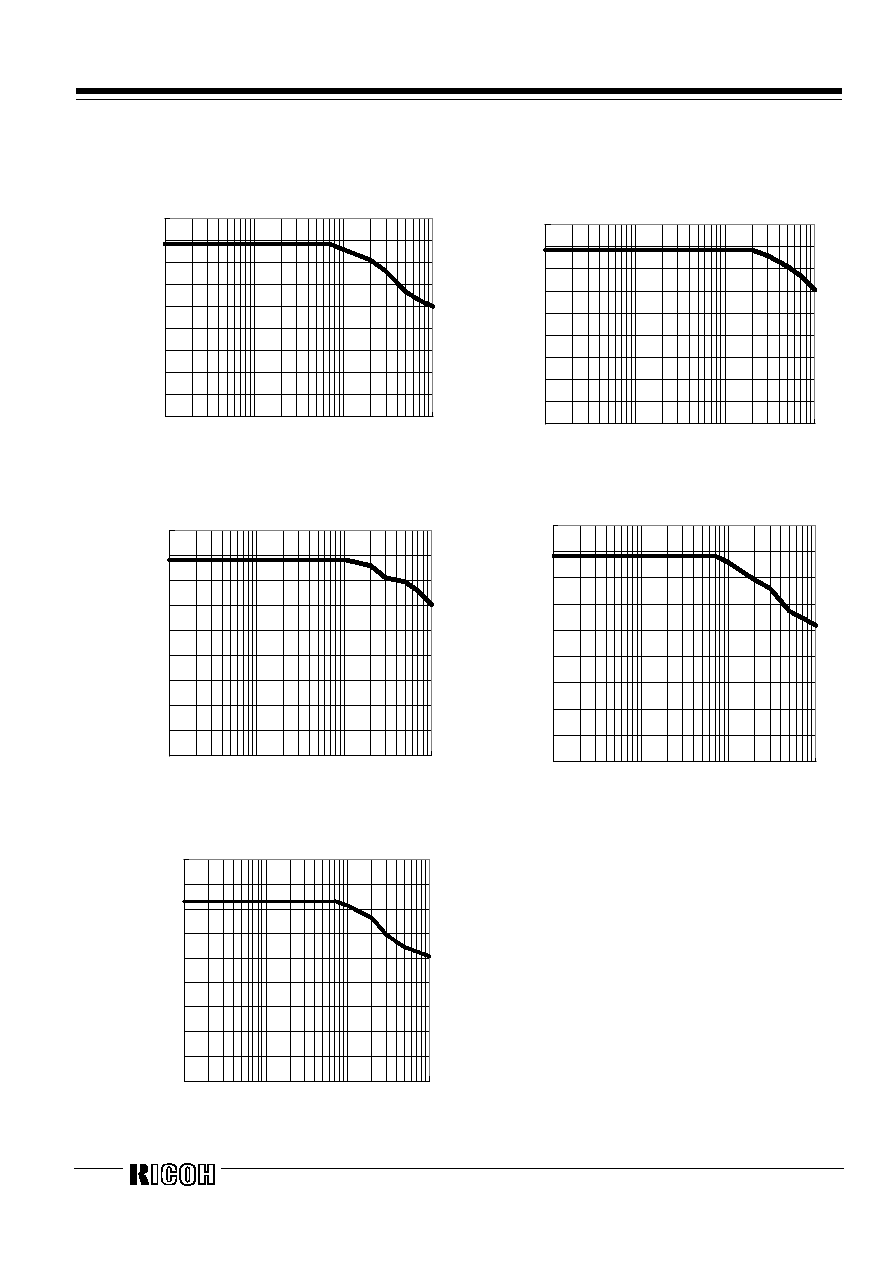
5)
Supply Current vs. Input Voltage
R11x2N151B
0
20
40
60
80
100
120
1
2
3
4
5
6
7
Input Voltage V
IN
[V]
Supply Current I
SS
{uA]
R11x2N201B
0
20
40
60
80
100
120
1
2
3
4
5
6
7
Input Voltage V
IN
[V]
Supply Current I
SS
{uA]
R11x2N301B
0
20
40
60
80
100
120
1
2
3
4
5
6
7
Input Voltage V
IN
[V]
Supply Current I
SS
{uA]
R11x2N401B
0
20
40
60
80
100
120
1
2
3
4
5
6
7
Input Voltage V
IN
[V]
Supply Current I
SS
{uA]
R11x2N501B
0
20
40
60
80
100
120
1
2
3
4
5
6
7
Input Voltage V
IN
[V]
Supply Current I
SS
{uA]

Rev. 1.10
- 15 -
6)
Supply Current vs. Temperature
R11x2N151A/B
0
50
100
150
200
-50
-25
0
25
50
75
100
Temperature Topt
Supply Current Iss(uA)
R11x2N201A/B
0
50
100
150
200
-50
-25
0
25
50
75
100
Temperature Topt
Supply Current Iss(uA)
R11x2N301A/B
0
50
100
150
200
-50
-25
0
25
50
75
100
Temperature Topt
Supply Current Iss(uA)
R11x2N401A/B
0
50
100
150
200
-50
-25
0
25
50
75
100
Temperature Topt
Supply Current Iss(uA)
R11x2N501A/B
0
50
100
150
200
-50
-25
0
25
50
75
100
Temperature Topt
Supply Current Iss(uA)
(
�
C)
V
IN
=2.5V C
IN
=1
m
F
C
OUT
=2.2
m
F
(
�
C)
V
IN
=3.0V C
IN
=1
m
F
C
OUT
=2.2
m
F
(
�
C)
V
IN
=4.0V C
IN
=1
m
F
C
OUT
=2.2
m
F
(
�
C)
V
IN
=5.0V C
IN
=1
m
F
C
OUT
=2.2
m
F
(
�
C)
V
IN
=6.0V C
IN
=1
m
F
C
OUT
=2.2
m
F
Rev. 1.10
- 16 -
7)
Ripple Rejection vs. Frequency
R11x2N151A/B
0.00
10.00
20.00
30.00
40.00
50.00
60.00
70.00
80.00
90.00
0.1
1
10
100
Frequency Freq [kHz]
Ripple Rejection RR [dB]
R11x2N201A/B
0.00
10.00
20.00
30.00
40.00
50.00
60.00
70.00
80.00
90.00
0.1
1
10
100
Frequency Freq [kHz]
Ripple Rejection RR [dB]
R11x2N301A/B
0.00
10.00
20.00
30.00
40.00
50.00
60.00
70.00
80.00
90.00
0.1
1
10
100
Frequency Freq [kHz]
Ripple Rejection RR [dB]
R11x2N401A/B
0.00
10.00
20.00
30.00
40.00
50.00
60.00
70.00
80.00
90.00
0.1
1
10
100
Frequency Freq [kHz]
Ripple Rejection RR [dB]
R11x2N501A/B
0.00
10.00
20.00
30.00
40.00
50.00
60.00
70.00
80.00
90.00
0.1
1
10
100
Frequency Freq [kHz]
Ripple Rejection RR [dB]
V
IN
=2.5V+0.5Vp-p
C
OUT
=2.2
m
F
I
OUT=30mA
V
IN
=3.0V+0.5Vp-p
C
OUT
=2.2
m
F
I
OUT=30mA
V
IN
=4.0V+0.5Vp-p
C
OUT
=2.2
m
F
I
OUT=30mA
V
IN
=5.0V+0.5Vp-p
C
OUT
=2.2
m
F
I
OUT=30mA
V
IN
=6.0V+0.5Vp-p
C
OUT
=2.2
m
F
I
OUT=30mA

Rev. 1.10
- 17 -
8) Ripple Rejection vs. Input Voltage (DC bias)
R11x2N301B
0.00
10.00
20.00
30.00
40.00
50.00
60.00
70.00
80.00
90.00
3.10
3.20
3.30
3.40
3.50
Input Voltage V
IN
[V]
Ripple Rejection RR[d
B
f=400Hz
f=1kHz
f=10kHz
R11x2N301B
0.00
10.00
20.00
30.00
40.00
50.00
60.00
70.00
80.00
90.00
3.10
3.20
3.30
3.40
3.50
Input Voltage V
IN
[V]
Ripple Rejection RR[dB
]
f=400Hz
f=1kHz
f=10kHz
R11x2N301B
0.00
10.00
20.00
30.00
40.00
50.00
60.00
70.00
80.00
90.00
3.10
3.20
3.30
3.40
3.50
Input Voltage V
IN
[V]
Ripple Rejection RR[dB]
f=400Hz
f=1kHz
f=10kHz
9) Input Transient Response
R11X2N151B Topt=25
�
C
C
OUT
=Ceramic 2.2
m
F
I
OUT=1mA
C
OUT
=Ceramic 2.2
m
F
I
OUT=10mA
C
OUT
=Ceramic 2.2
m
F
I
OUT=50mA
V
IN
=2.5V<-->3.5V
I
OUT
=30mA
C
IN
=none
C
OUT
=2.2
m
F
tr/tf=5
m
s
V
IN
V
OUT

Rev. 1.10
- 18 -
R11X2N201B Topt=25
�
C
R11X2N301B Topt=25
�
C
R11X2N401B Topt=25
�
C
V
IN
=3.0V<-->4.0V
I
OUT
=30mA
C
IN
=none
C
OUT
=2.2
m
F
tr/tf=5
m
s
V
IN
V
OUT
V
OUT
V
IN
V
IN
=4.0V<-->5.0V
I
OUT
=30mA
C
IN
=none
C
OUT
=2.2
m
F
tr/tf=5
m
s
V
IN
=5.0V<-->6.0V
I
OUT
=30mA
C
IN
=none
C
OUT
=2.2
m
F
tr/tf=5
m
s
V
IN
V
OUT

Rev. 1.10
- 19 -
R11X2N501B Topt=25
�
C
10) Load Transient Response
R11X2N151B Topt=25
�
C
R11X2N201B Topt=25
�
C
V
IN
V
OUT
V
IN
=6.0V<-->7.0V
I
OUT
=30mA
C
IN
=none
C
OUT
=2.2
m
F
tr/tf=5
m
s
I
OUT
V
OUT
I
OUT
=50mA<-->100mA
V
IN
=2.5V
C
IN
=2.2
m
F
C
OUT
=2.2
m
F
tr/tf=5 s
I
OUT
V
OUT
I
OUT
=50mA<-->100mA
V
IN
=3.0V
C
IN
=2.2
m
F
C
OUT
=2.2
m
F
tr/tf=5
m
s

Rev. 1.10
- 20 -
R11X2N301B Topt=25
�
C
R11X2N401B Topt=25
�
C
R11X2N501B Topt=25
�
C
I
OUT
=50mA<-->100mA
V
IN
=4.0V
C
IN
=2.2
m
F
C
OUT
=2.2
m
F
tr/tf=5
m
s
I
OUT
V
OUT
I
OUT
=50mA<-->100mA
V
IN
=5.0V
C
IN
=2.2
m
F
C
OUT
=2.2
m
F
tr/tf=5
m
s
I
OUT
I
OUT
V
OUT
V
OUT
I
OUT
=50mA<-->100mA
V
IN
=6.0V
C
IN
=2.2
m
F
C
OUT
=2.2
m
F
tr/tf=5
m
s

Rev. 1.10
- 21 -
n
TECHNICAL NOTES
When using these ICs, be sure to consider following points:
l
Make V
DD
and GND line sufficient. When the impedance of these is high, there is a case to pick up the noise or not to work
correctly.
l
Connect the capacitor with a capacitance as much as 2.2
mF between V
DD
and GND as close as possible.
l
Set external components, especially Output Capacitor, as close as possible to the ICs and make wiring shortest.
In these ICs, phase compensation is made for securing stable operation even if the load current is varied. For this purpose, be
sure to use a capacitor C
OUT
with good frequency characteristics and ESR (Equivalent Series Resistance) of which is in the
range described as follows:
3
4
1
2
R1122NXX1B
CE
VDD
VOUT
GND
ESR
Ceramic
Cap.
IOUT
S.A.
Spectrum
Analyzer
VIN
Ceramic
Cap.
Measuring Circuit for white noise; R1122NXX1B
The relations between I
OUT
(Output Current) and ESR of Output Capacitor are shown below. The conditions when the white
noise level is under 40
mV(Avg.) are marked as the hatched area in the graph.
(note: When the additional ceramic capacitors are connected to the Output Pin with Output capacitor for phase compensation,
the operation might be unstable. Because of this, test these ICs with as same external components as ones to be used on the
PCB.)
<measuring conditions>
(1) V
IN
=V
OUT
+1V
(2) Frequency band :10Hz to 1MHz
(3) Temperature : 25
�C

Rev. 1.10
- 22 -
R11X2N151B
R11X2N151B
C
OUT
=2.2uF,C
IN
=2.2uF
0.01
0.1
1
10
100
0
30
60
90
120
150
I
OUT
[mA]
ESR[Ohm]
C
OUT
=4.7uF,C
IN
=2.2uF
0.01
0.1
1
10
100
0
30
60
90
120
150
I
OUT
[mA]
ESR[Ohm]
R11X2N301B
R11X2N301B
C
OUT
=2.2uF,C
IN
=2.2uF
0.01
0.1
1
10
100
0
30
60
90
120
150
I
OUT
[mA]
ESR[Ohm]
C
OUT
=4.7uF,C
IN
=2.2uF
0.01
0.1
1
10
100
0
30
60
90
120
150
I
OUT
[mA]
ESR[Ohm]