
LOW NOISE 150mA LDO REGULATOR
R1126N SERIES
1
OUTLINE
The R1126N Series are CMOS-based voltage regulator ICs with high output voltage accuracy, extremely low
supply current, low ON-resistance, and high ripple rejection. Each of these ICs consists of a voltage reference
unit, an error amplifier, resistor-net for voltage setting, a current limit circuit, and a chip enable circuit.
These ICs perform with low dropout voltage and a chip enable function. The line transient response and load
transient response of the R1126N Series are excellent, thus these ICs are very suitable for the power supply for
hand-held communication equipment.
The output voltage of these ICs is fixed with high accuracy. Since the package for these ICs is SOT-23-5, high
density mounting of the ICs on boards is possible.
FEATURES
∑
Low Supply Current..............................................................Typ. 10
µ
A
∑
Standby Mode ......................................................................Typ. 0.1
µ
A
∑
Low Dropout Voltage ............................................................Typ. 0.29V (I
OUT
=150mA 3.0V Output type)
∑
High Ripple Rejection...........................................................Typ. 70dB (f
=
1kHz 2.8V Output type)
..............................................................................................Typ. 53dB (f
=
10kHz)
∑
Low Temperature-Drift Coefficient of Output Voltage...........Typ.
±
100ppm/
∞
C
∑
Excellent Line Regulation.....................................................Typ. 0.02%/V
∑
High Output Voltage Accuracy..............................................
±1
.5%(2.8V Output Type)
∑
Small Packages ..................................................................SOT-23-5
∑
Input Voltage Range................................................................ 1.8V to 6.0V
∑
Output Voltage......................................................................Stepwise setting with a step of 0.1V in
the range of 1.5V to 4.0V is possible
∑
Built-in Fold Back Protection Circuit.....................................Typ. 40mA (Current at short mode)
∑
Ceramic capacitors are recommended to be used with this IC ....C
IN
=
C
OUT
=
1
µ
F
APPLICATIONS
∑
Power source for portable communication equipment.
∑
Power source for electrical appliances such as cameras, VCRs and camcorders.
∑
Power source for battery-powered equipment.
R1126N
2
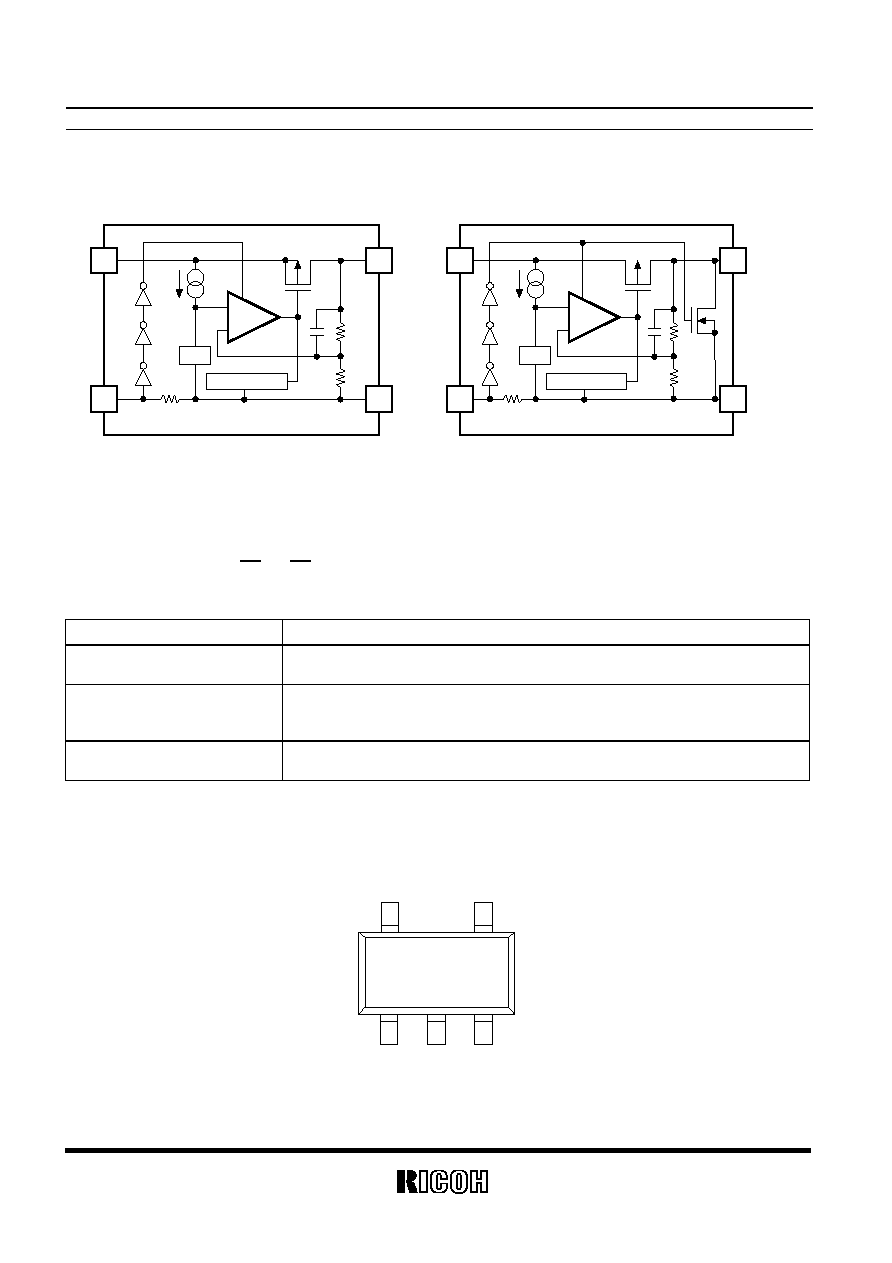
BLOCK DIAGRAMS
R1126Nxx1B
R1126Nxx1D
V
OUT
GND
V
DD
CE
Vref
Current Limit
+
-
V
OUT
GND
V
DD
CE
Vref
Current Limit
+
-
SELECTION GUIDE
The output voltage, version, and the taping type for the ICs can be selected at the user's request.
The selection can be made with designating the part number as shown below;
R1126Nxx1x-xx
Part Number
a b c
Code Contents
a
Setting Output Voltage (V
OUT
):
Stepwise setting with a step of 0.1V in the range of 1.5V to 4.0V is possible
b
Designation of Active Type:
B: active high type
D: active high, with auto discharge
c
Designation of Taping Type:
Ex. TR (refer to Taping Specifications; TR type is the standard direction.)
PIN CONFIGURATION
z SOT-23-5
1
2
3
5
4
(mark side)
R1126N
4
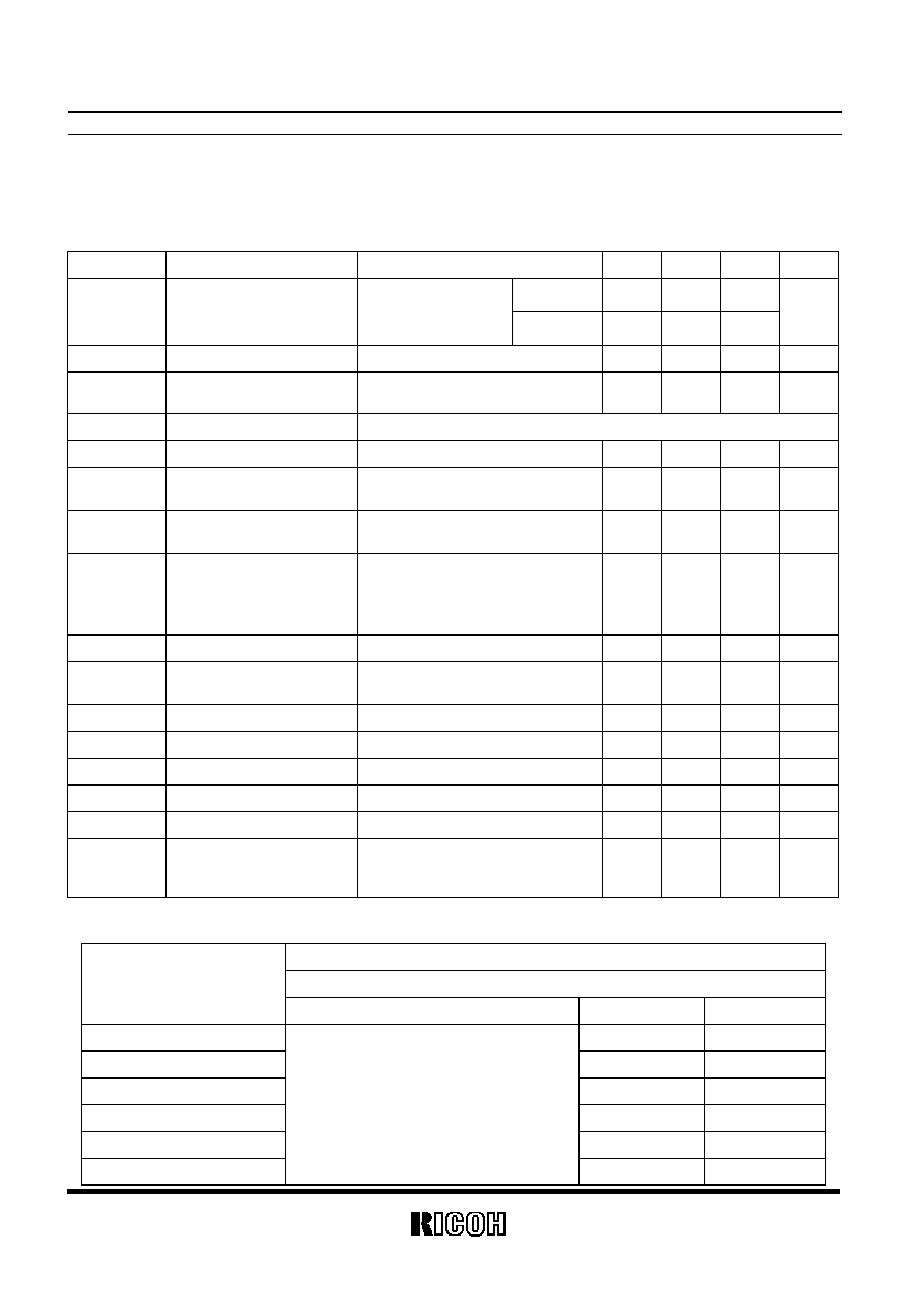
ELECTRICAL CHARACTERISTICS
∑
R1126Nxx1B/D
Topt
=
25
∞
C
Symbol Item
Conditions Min.
Typ.
Max.
Unit
V
OUT
3.0V
◊
0.985
◊
1.015
V
OUT
Output
Voltage
V
IN
=
Set V
OUT
+
1V
1mA
<
=
I
OUT
<
=
30mA V
OUT
>3.0
◊
0.985
◊
1.015
V
I
OUT
Output
Current
V
IN
-
V
OUT
=
1.0V
150 mA
V
OUT
/
I
OUT
Load Regulation
V
IN
=
Set V
OUT
+
1V
1mA
<
=
I
OUT
<
=
150mA
30 80
mV
V
DIF
Dropout
Voltage
Refer to the ELECTRICAL CHARACTERISTICS by OUTPUT VOLTAGE
I
SS
Supply
Current
V
IN
=
Set V
OUT
+
1V, I
OUT
=
0mA
10
µ
A
Istandby
Supply Current
(Standby)
V
IN
=
Set V
OUT
+
1V
V
CE
=
GND
0.1
1.0
µ
A
V
OUT
/
V
IN
Line Regulation
Set V
OUT
+
0.5V
<
=
V
IN
<
=
6.0V
I
OUT
=
30mA
0.02
0.10
%/V
RR Ripple
Rejection
f
=
1kHz
f
=
10kHz
Ripple 0.2Vp
-
p
V
IN
-
V
OUT
=
1.0V, I
OUT
=
30mA
70
53
dB
V
IN
Input
Voltage
1.8 6.0 V
V
OUT
/
T
Output Voltage
Temperature Coefficient
I
OUT
=
30mA
-
40
∞
C
<
=
Topt
<
=
85
∞
C
±
100
ppm
/
∞
C
I
LIM
Short Current Limit
V
OUT
=
0V
40 mA
I
PD
CE
Pull-down
Current
0.5
µ
A
V
CEH
CE Input Voltage "H"
1.0
V
IN
V
V
CEL
CE Input Voltage "L"
0.0
0.3
V
en Output
Noise
BW
=
10Hz to 100kHz
30
µ
Vrms
R
LOW
On Resistance of Nch for
auto-discharge
(Only for D version)
V
CE
=
0V
70
∑
ELECTRICAL CHARACTERISTICS by OUTPUT VOLTAGE
Topt
=
25
∞
C
Dropout Voltage
V
DIF
(V)
Output Voltage
V
OUT
(V)
Condition Typ.
Max.
V
OUT
=
1.5
0.54 0.86
1.5V<V
OUT
1.6V
0.50 0.75
1.6V<V
OUT
1.7V
0.46 0.70
1.7V< V
OUT
<
=
2.0V 0.44
0.65
2.0V<V
OUT
<
=
2.7V 0.37
0.56
2.7V<V
OUT
<
=
4.0V
I
OUT
=
150mA
0.29 0.46

R1126N
5
In terms of typical characteristics, please refer to the data sheet of R1116x Series.
TECHNICAL NOTES
When using these ICs, consider the following points:
Phase Compensation
In these ICs, phase compensation is made for securing stable operation even if the load current is varied. For
this purpose, use a capacitor C
OUT
with good frequency characteristics and ESR (Equivalent Series Resistance).
(Note: When the additional ceramic capacitors are connected to the output pin with an output capacitor for
phase compensation, the operation might be unstable. Because of this, test these ICs with as same external
components as ones to be used on the PCB.)
PCB Layout
Make V
DD
and GND lines sufficient. If their impedance is high, noise pickup or unstable operation may result.
Connect a capacitor with a capacitance value as much as 1.0µF or more between V
DD
and GND pin, and as
close as possible to the pins.
Set external components, especially the output capacitor, as close as possible to the ICs, and make wiring as
short as possible
