
300mA LDO REGULATOR
R1130xxxxA/B/C SERIES
1
OUTLINE
The R1130xxxxx Series are CMOS-based voltage regulator (VR) ICs. VR function has features of high ripple rejec-
tion, low dropout voltage, high output voltage accuracy, and ultra-low supply current. Each of these ICs consists of a
voltage reference unit, an error amplifier, resistors for setting output voltage, and a current limit circuit. Each of the
R1130xxxxA/B type includes also a chip enable circuit.
The output voltage of the R1130xxxxC type is adjustable with external resistors.
The output voltage of R1130xxxxA/B is fixed in the IC. Low supply current by the merit of CMOS process and
built-in transistors with low ON-resistance make low dropout voltage. These regulators in the R1130xxxxx Series are
remarkable improvement on the current regulators in terms of ripple rejection, input transient response, and load
transient response. Maximum Output Current is large for its compact size.
Thus, the R1130xxxxx series are suitable for power supply for CD-drives, DVD-drives, and so forth.
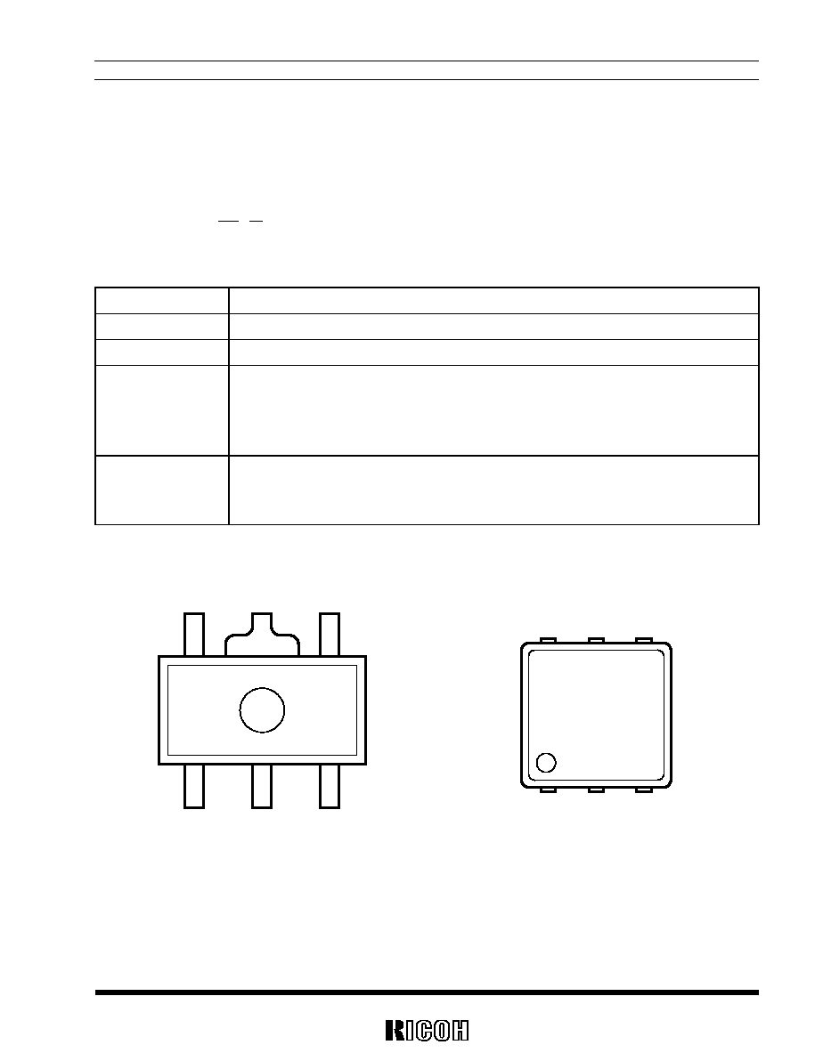
Since the packages for these ICs are the SOT-89-5 package or HSON-6P, high density mounting of the ICs on
boards is possible.
FEATURES
∑ Ultra-Low Supply Current
...................................................................................
Typ. 50µA
∑ Low Standby Current
.................................................................................................
Typ. 0.1µA (VR) for A type
∑ High Ripple Rejection
................................................................................................
Typ. 60dB (f=1kHz) (VR)
∑ Output Current
.................................................................................................................
Min. 300mA (V
IN
=V
OUT
+1V)
∑ Output Voltage (VR)
....................................................................................................
Stepwise setting with a step of 0.1V in the range of 1.5V to
5.0V (A/B Version) (Reference 1.8V (C Version))
∑ High Output Voltage Accuracy
........................................................................
±2.0% (VR) for A/B type,
±2.0% (Reference Voltage for adjustable VR) for C type
∑ Low Dropout Voltage
..................................................................................................
Typ. 0.2V (I
OUT
=100mA) (VR)
∑ Small Package
.....................................................................................................................
SOT-89-5, HSON-6P
∑ Built-in Current Limit Circuit
∑ Low Temperature-drift Coefficient of Output Voltage
..........
Typ. ±100ppm/∞C
∑ Absolute Maximum Voltage
................................................................................
9V
∑ Internal Phase Compensation (small output capacitance such as 0.1µF Ceramic can be used with.)
APPLICATIONS
∑ Power source for CD-drives and DVD-drives, HDD.
∑ Local Power source for Notebook PC.
NO. EA-078-0305
R1130xxxxA/B/C
3
SELECTION GUIDE
The output voltage, chip-enable polarity, the taping type can be selected at the user's request. The selection can be
made with designating the part number as follows;
R1130xxxxx-xx Part Number
a b c d
Code
Contents
a
Package Type; H: SOT-89-5, D: HSON-6P
b
Serial Number for Voltage Setting
c
Designation of option;
A: Fixed Output Voltage Regulator with
----
CE pin ("L" enable)
B: Fixed Output Voltage Regulator with CE pin ("H" enable)
C: Output Voltage Adjustable Regulator with CE pin ("H" enable)
d
Designation of Taping Type;
T1 or T2 (Refer to Taping Specifications) for SOT-89-5
TR or TL for HSON-6P
PIN CONFIGURATION
SOT-89-5
HSON-6P
5
4
Mark Side
1
2
3
3
Mark side
2
1
4
5
6

R1130xxxxA/B/C
4
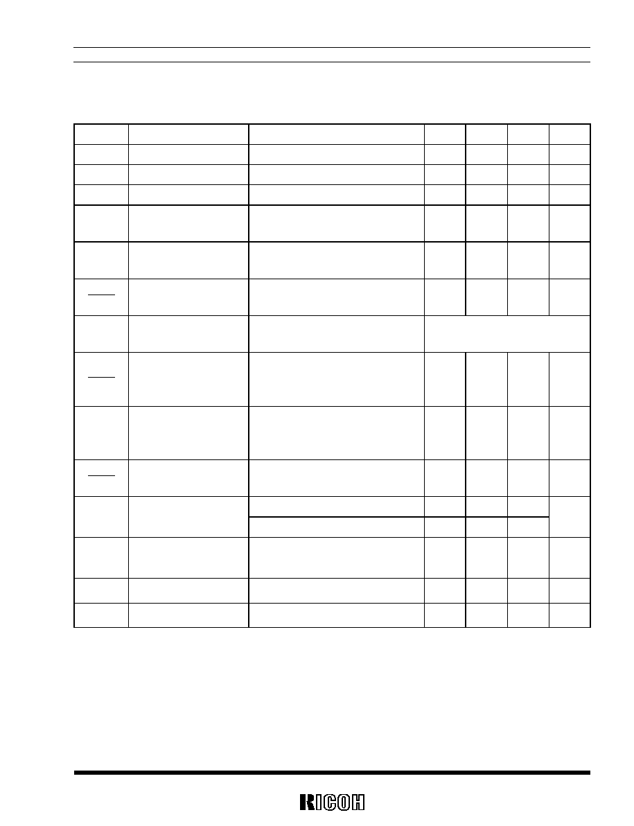
PIN DESCRIPTION
SOT-89-5
Pin No.
Symbol
Description
1
V
OUT
Voltage Regulator Output Pin
2
V
DD
Input Pin
3
GND
Ground Pin
N.C. (A/B type)
No Connection
4
ADJ (C type)
Adjustable Regulator feedback Input Pin (Connect to resistor voltage divider.)
5
----
CE (A type)
or CE (B/C type)
Chip Enable Pin
HSON-6P
Pin No.
Symbol
Description
1
V
DD
Input Pin
2
GND
Ground Pin
N.C. (A/B type)
No Connection
3
ADJ (C type)
Adjustable Regulator feedback Input Pin (Connect to resistor voltage divider.)
4
N.C.
No Connection
5
----
CE (A type)
or CE (B/C type)
Chip Enable Pin
6
V
OUT
Voltage Regulator Output Pin
ABSOLUTE MAXIMUM RATINGS
Symbol
Item
Rating
Unit
V
IN
Input Voltage
9.0
V
V
CE
Input Voltage (
----
CE or CE Input Pin)
-0.3 ~ V
IN
+0.3
V
V
ADJ
Input Voltage (ADJ Input Pin)
-0.3 ~ V
IN
+0.3
V
V
OUT
Output Voltage
-0.3 ~ V
IN
+0.3
V
I
OUT
Output Current
450
mA
P
D
Power Dissipation (SOT-89-5)
500
mW
P
D
Power Dissipation (HSON-6P)
400
mW
Topt
Operating Temperature
-40 ~ 85
∞C
Tstg
Storage Temperature
-55 ~ 125
∞C
R1130xxxxA/B/C
5
ELECTRICAL CHARACTERISTICS
∑ R1130xxxxA
(Topt=25∞C)
Symbol
Item
Conditions
Min.
Typ.
Max.
Unit
V
IN
Input Voltage
2.5
8.0
V
I
SS1
Supply Current 1
V
IN
-V
OUT
=1.0V V
IN
=GND
50
100
µA
Istby
Standby Current
V
IN
-V
OUT
=1.0V V
IN
=V
CE
0.1
1.0
µA
V
OUT
Output voltage
V
IN
-V
OUT
=1.0V
1mAI
OUT
80mA
x0.98
Set
V
OUT
x1.02
V
I
OUT1
Output Current
Refer to the table of Input Voltage by
Set Output Voltage
300
mA
V
OUT
I
OUT
Load regulation
V
IN
-V
OUT
=1.0V
1mAI
OUT
80mA
40
80
mV
V
DIF
Dropout Voltage
I
OUT
=100mA
Refer to the Table of Dropout Volt-
age by Set Output Voltage
V
OUT
V
IN
Line regulation
I
OUT
=80mA,
Set V
OUT
2.0V: V
OUT
+0.5VV
IN
8.0V
Set V
OUT
1.9V: 2.5VV
IN
8.0V
0.1
0.2
%/V
RR
Ripple Rejection
f=1kHz, Ripple 0.5Vp-p, I
OUT
=80mA
Set V
OUT
1.8V: V
IN
-V
OUT
=1.0V
Set V
OUT
1.7V: V
IN
=2.8V
60
dB
V
OUT
T
Output Voltage
Temperature Coefficient
I
OUT
=10mA, V
IN
-V
OUT
=1.0V
-40∞CTopt85∞C
±100
ppm
/∞C
Set V
OUT
3.9V, V
OUT
=0V
70
Ilim
Short Current Limit
Set V
OUT
4.0V, V
OUT
=0V
50
mA
R
PU
Pull-up resistance for
----
CE pin
2.5
5.0
10.0
M
V
CEH
----
CE Input Voltage "H"
V
IN
=2.5V
1.5
V
IN
V
V
CEL
----
CE Input Voltage "L"
V
IN
=2.5V
0.00
0.25
V
