 | –≠–ª–µ–∫—Ç—Ä–æ–Ω–Ω—ã–π –∫–æ–º–ø–æ–Ω–µ–Ω—Ç: R1131 | –°–∫–∞—á–∞—Ç—å:  PDF PDF  ZIP ZIP |

300mA Low Voltage LDO REGULATOR
R1131x SERIES
1
1
OUTLINE
The R1131x Series are CMOS-based low voltage regulator ICs with output voltage range from 0.8V to 3.3V. The
minimum operating voltage is 1.4V. Each of these voltage regulator ICs consists of a voltage reference unit, an error
amplifier, resistors for setting output voltage, a current limit circuit, and a chip enable circuit.
To prevent the destruction by over current, current limit circuit is included. Standby mode realizes ultra small
consumption current.
The output voltage of these ICs is internally fixed with high accuracy. Since the packages for these ICs are SOT-23-5,
SON-6, and HSON-6, high density mounting of the ICs on boards is possible.
FEATURES
∑
Ultra-Low Supply Current .....................................................Typ. 80
µ
A (V
OUT
<1.8V)
..............................................................................................Typ.
60
µ
A (
VOUT
1.8V)
∑
Standby Mode.......................................................................Typ. 0.1
µ
A
∑
Low Dropout Voltage ............................................................Typ. 0.48V(I
OUT
=300mAOutput Voltage=1.0V Type)
..............................................................................................Typ.
0.31V(I
OUT
=300mAOutput Voltage=1.5V Type)
..............................................................................................Typ.
0.23V(I
OUT
=300mAOutput Voltage=3.0V Type)
∑
High Ripple Rejection ...........................................................Typ. 65dB (f
=
1kHz)
∑
Low Temperature-Drift Coefficient of Output Voltage ...........Typ.
±
100ppm/
∞
C
∑
Excellent Line Regulation .....................................................Typ. 0.01%/V
∑
High Output Voltage Accuracy..............................................
±
2.0%
∑
Small Packages ..................................................................SOT-23-5 (Super Mini-mold) / SON-6 / HSON-6
∑
Output Voltage .................................................. Stepwise setting with a step of 0.1V in the range of 0.8V to 3.3V
∑
Input Voltage.........................................................................Min.1.40V
∑
Built-in fold-back Protection Circuit.......................................Typ. 50mA (Current at short mode)
∑
External Capacitor ................................................................C
IN
=
C
OUT
=
Tantalum 1.0
µ
F (V
OUT
<1.0V)
..............................................................................................C
IN
=
C
OUT
=
Ceramic 1.0
µ
F (V
OUT
1.0V)
APPLICATIONS
∑
Precision Voltage References.
∑
Power source for electrical appliances such as cameras, VCRs and hand-held communication equipment.
∑
Power source for battery-powered equipment.

R1131x
2
BLOCK DIAGRAMS
R1131xxxxA
R1131xxxxB
V
OUT
GND
Vref
CE
Vref
Current
V
DD
+
-
Vref
Current
+
-
V
OUT
GND
CE
V
DD
R1131xxxxD
Vref
Current
+
-
V
OUT
GND
CE
V
DD
SELECTION GUIDE
The output voltage, the chip enable polarity, package type, and the taping type for the ICs can be selected at the user's
request. The selection can be available by designating the part number as shown below;
R1131xxxxx-xx
Part Number
a
b
a'
c
d
Code Contents
a ,a'
Designation of Package Type:
R1131Nxx1x-xx : SOT-23-5(Mini-mold)
R1131Dxx1x-xx : SON-6
R1131Dxx2x-xx : HSON-6
B
Setting Output Voltage (V
OUT
):
Stepwise setting with a step of 0.1V in the range of 0.8V to 3.3V is possible.
If the output=1.85V, then the code is R1131x18xx5. If the output=2.85, then
the code is R1131x28xx5.
C
Designation of Chip Enable Option:
A: "L" active type
B: "H" active type
D: "H" active and with auto discharge function
D
Designation of Taping Type: TR
Refer to Taping Specifications

R1131x
3
PIN CONFIGURATION
z
SOT-23-5
z
SON-6
q
q
q
q
HSON-6
1
2
3
5
4
(mark side)
1
2
3
6
5
4
6
5
4
1
2
3
PIN DESCRIPTIONS
∑
R1131N
Pin No.
Symbol
Description
1 V
DD
Input
Pin
2 GND
Ground
Pin
3
CE or CE
Chip Enable Pin
4 NC
No
Connection
5 V
OUT
Output
pin
∑
R1131D
Pin No.
Symbol
Description
1 V
DD
Input
Pin
2 NC
No
Connection
3 V
OUT
Output
pin
4 NC
No
Connection
5 GND
Ground
Pin
6
CE or CE
Chip Enable Pin
*Tabs and tab suspension leads could be short to the GND level.

R1131x
4
ABSOLUTE MAXIMUM RATINGS
Symbol Item
Rating Unit
V
IN
Input
Voltage
6.5
V
V
CE
Input Voltage ( CE or CE Pin)
-
0.3 ~ 6.5
V
V
OUT
Output
Voltage
-
0.3 ~ V
IN
+
0.3
V
I
OUT
Output
Current
350
mA
250(SOT-23-5/SON-6) mW
P
D
Power
Dissipation
400(HSON-6) mW
Topt
Operating Temperature Range
-
40 ~ 85
∞
C
Tstg
Storage Temperature Range
-
55 ~ 125
∞
C
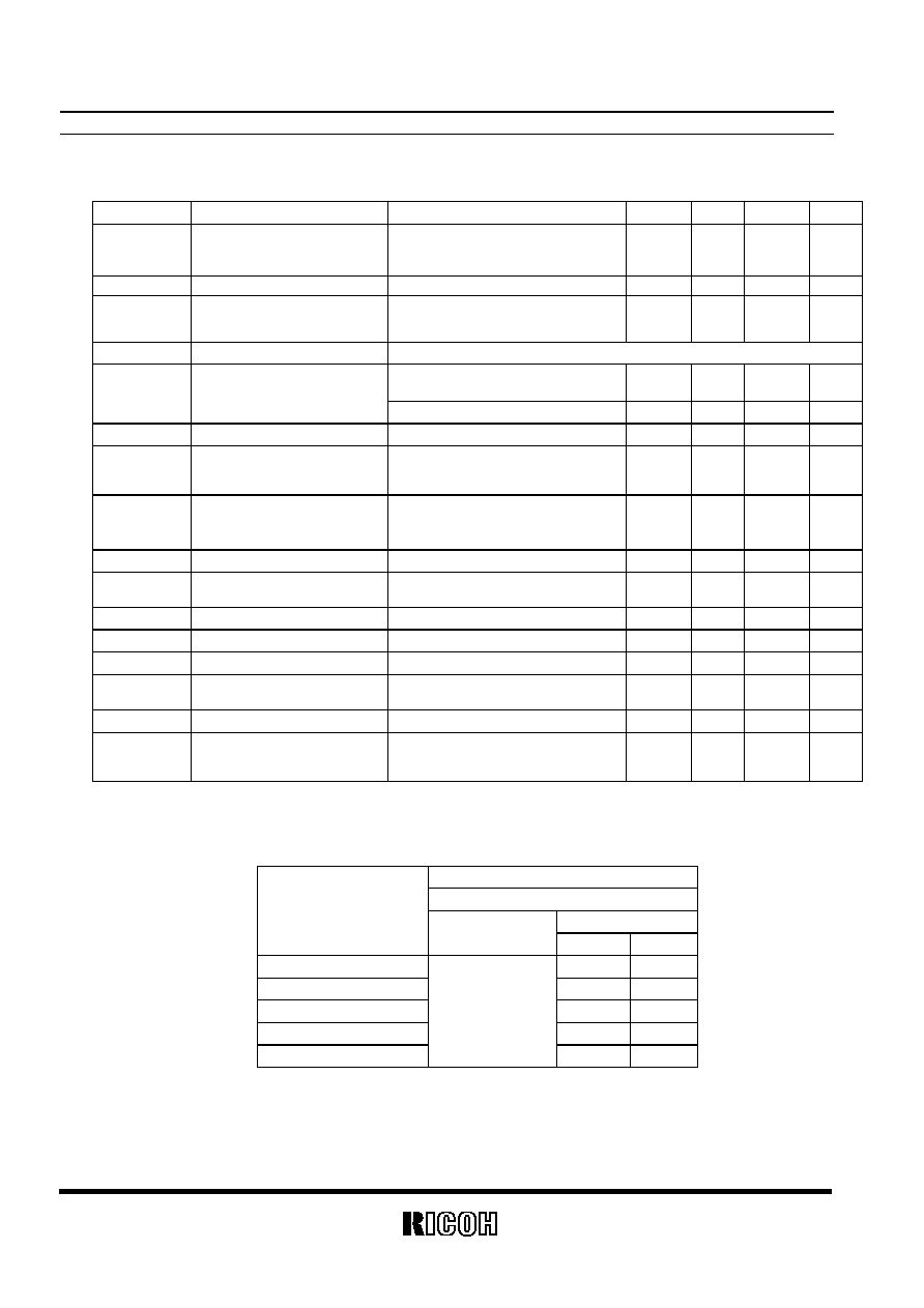
ELECTRICAL CHARACTERISTICS
∑
R1131xxxxA
Topt
=
25
∞
C
Symbol Item
Conditions Min.
Typ.
Max.
Unit
V
OUT
Output Voltage
V
IN
=
Set V
OUT
+
1V
1
µ
A
<
=
I
OUT
<
=
30mA (Note 1)
V
OUT
◊
0.98
(-30mV)
V
OUT
◊
1.02
(30mV)
V
I
OUT
Output Current
V
IN
-
V
OUT
=
1.0V
300 mA
V
OUT
/
I
OUT
Load Regulation
V
IN
=
Set V
OUT
+
1V
1mA
<
=
I
OUT
<
=
300mA
40
70
mV
V
DIF
Dropout Voltage
Refer to the ELECTRICAL CHARACTERISTICS by OUTPUT VOLTAGE
V
IN
=
Set V
OUT
+
1V, V
OUT
<1.8V
80
111
µ
A
I
SS1
Supply Current
V
IN
=
Set V
OUT
+
1V, V
OUT
1.8V
60
90
µ
A
Istandby
Supply Current (Standby)
V
IN
=
V
CE
=
Set V
OUT
+
1V
0.1
1.0
µ
A
V
OUT
/
V
IN
Line Regulation
Set V
OUT
+ 0.5V
<
=
V
IN
<
=
6.0V
I
OUT
= 30mA,
Set V
OUT
< 0.9V: 1.4V
<
=
V
IN
<
=
6.0V
0.01
0.15
%/V
RR
Ripple Rejection
f = 1kHz, Ripple 0.2Vp-p
V
IN
= Set V
OUT
+ 1V, I
OUT
= 30mA
65
dB
V
IN
Input Voltage
1.4 6.0
V
V
OUT
/
T
Output Voltage Temperature
Coefficient
I
OUT
=
30mA
-
40
∞
C
<
=
Topt
<
=
85
∞
C
±
100
ppm
/
∞
C
I
LIM
Short Current Limit
V
OUT
=
0V
50
mA
R
PU
CE
Pull-up Resistance
1.87 5.00 12.00
M
V
CEH
CE
Input Voltage "H"
1.0
6.0
V
V
CEL
CE
Input Voltage "L"
0.0 0.3
V
V
EN
Output Noise
BW = 10Hz to 100kHz
30
µ
Vrms
Note1: ±30mV tolerance for V
OUT
<
=
1.5V.
R1131x
5
∑
R1131xxxxB/D ...........................................
Topt
=
=
=
=
25
∞
∞
∞
∞
C
Symbol Item
Conditions Min.
Typ.
Max.
Unit
V
OUT
Output Voltage
V
IN
=
Set V
OUT
+
1V
1
µ
A
<
=
I
OUT
<
=
30 mA (Note 1)
V
OUT
◊
0.98
(-30mV)
V
OUT
◊
1.02
(30mV)
V
I
OUT
Output Current
V
IN
-
V
OUT
=
1.0V
300 mA
V
OUT
/
I
OUT
Load Regulation
V
IN
=
Set V
OUT
+
1V
1mA
<
=
I
OUT
<
=
300mA
40
70
mV
V
DIF
Dropout Voltage
Refer to the ELECTRICAL CHARACTERISTICS by OUTPUT VOLTAGE
V
IN
=
Set V
OUT
+
1V, V
OUT
<1.8V
80
111
µ
A
I
SS1
Supply Current
V
IN
=
Set V
OUT
+
1V, V
OUT
1.8V
60
90
µ
A
Istandby
Supply Current (Standby)
V
IN
=
Set V
OUT
+
1V,V
CE
= GND
0.1
1.0
µ
A
V
OUT
/
V
IN
Line Regulation
Set V
OUT
+0.5V
<
=
V
IN
<
=
6.0V
I
OUT
= 30mA
Set V
OUT
< 0.9V :1.4V
<
=
V
IN
<
=
6.0V
0.01
0.15
%/V
RR
Ripple Rejection
f = 1kHz, Ripple 0.2Vp-p
V
IN
= Set V
OUT
+ 1V, I
OUT
= 30mA
65
dB
V
IN
Input Voltage
1.4 6.0
V
V
OUT
/
T
Output Voltage Temperature
Coefficient
I
OUT
=
30mA
-
40
∞
C
<
=
Topt
<
=
85
∞
C
±
100
ppm
/
∞
C
I
LIM
Short Current Limit
V
OUT
=
0V
50
mA
R
PDC
CE Pull-down Resistance
1.87 5.00 12.00
M
V
CEH
CE Input Voltage "H"
1.0
V
IN
V
V
CEL
CE Input Voltage "L"
0.0 0.3
V
V
EN
Output Noise
BW=10Hz to 100kHz
30
µ
Vrms
R
LOW
Nch On Resistance for auto
discharge (applied to D
version only)
V
CE
= 0V
60
Note1: ±30mV tolerance for V
OUT
<
=
1.5V.
ELECTRICAL CHARACTERISTICS by OUTPUT VOLTAGE
Topt
=
25
∞
C
Dropout Voltage
V
DIF
(V)
V
DIF
Output Voltage V
OUT
(V)
Condition
Typ.
Max.
0.8
=
V
OUT
0.620
0.850
0.9
=
V
OUT
0.550
0.780
1.0
<
=
V
OUT
<
=
1.5
0.480
0.700
1.5
<
=
V
OUT
<
=
2.6
0.310
0.450
2.6
<
=
V
OUT
I
OUT
=
300mA
0.230
0.350

R1131x
6
TECHNICAL NOTES
When using these ICs, consider the following points:
Phase Compensation
In these ICs, phase compensation is made for securing stable operation even if the load current is varied. For this
purpose, be sure to use 1.0
µ
F or more capacitor C
OUT
with good frequency characteristics and ESR (Equivalent Series
Resistance).
(Note: If a tantalum capacitor is connected to the Output pin for phase compensation, if the ESR value of the capacitor is
too large, the operation might be unstable. Because of this, test these ICs with as same external components as ones to
be used on the PCB.)
Chip capacitor characteristics of Bias dependence and Temperature characteristics may vary depending on its size,
manufacturer, and part number.
PCB Layout
Make V
DD
and GND lines sufficient. If their impedance is high, pick-up the noise or unstable operation may result.
Connect a capacitor with as much as 1.0
µ
F capacitor between V
DD
and GND pin as close as possible.
Set external components, especially the output capacitor, as close as possible to the ICs, and make wiring as short as
possible.
TYPICAL APPLICATION
C1
C2
V
IN
A
I
OUT
VDD
OUT
CE
GND
R1131xxxxx
SERIES
External Components examples: CM05X5R105K06AB (Kyocera)
C1005JBOJ105K (TDK)
GRM155B30J105KE18B (Murata)
Output Capacitor; 1.0
µ
F or more capacity ceramic Type (If V
OUT
<1.0V, Tantalum Type is recommended)
Input Capacitor, 1.0
µ
F or more capacity ceramic Type

R1131x
7
TYPICAL CHARACTERISTICS
1) Output Voltage vs. Output Current (Topt
=
25
∞
C)
R1131x08xx
R1131x15xx
0.0
0.2
0.4
0.6
0.8
1.0
0
200
400
600
O utput Current Iout (m A)
O
u
t
put
Vol
t
age Vout
(
V
)
0.0
0.2
0.4
0.6
0.8
1.0
1.2
1.4
1.6
0
200
400
600
Output Current Iout(mA)
O
u
t
put
V
o
l
t
age
V
out
(
V
)
R1131x26xx
R1131x33xx
0.0
0.5
1.0
1.5
2.0
2.5
3.0
0
100
200
300
400
500
600
Output Current Iout(mA)
O
u
t
put
V
olt
age
V
out
(
V
)
0.0
0.5
1.0
1.5
2.0
2.5
3.0
3.5
0
200
400
600
Output Current Iout(mA)
Out
p
ut
Volt
age
Vout
(V)
2) Output Voltage vs. Input Voltage
R1131x08xx
R1131x15xx
0.0
0.1
0.2
0.3
0.4
0.5
0.6
0.7
0.8
0.9
1.0
0
1
2
3
4
5
6
Input Voltage Vin(V)
O
u
tput Voltage
Vout(
V
)
IOUT=1mA
IOUT=30mA
IOUT=50mA
0.0
0.2
0.4
0.6
0.8
1.0
1.2
1.4
1.6
0
1
2
3
4
5
6
Input Voltage Vin(V)
O
u
t
put
V
o
lt
age
V
out
(V
)
IOUT=1mA
IOUT=30mA
IOUT=50mA
1.45V
V
IN
=2.8V
1.8V
V
IN
=3.5V
V
IN
=4.6V
2.9V
V
IN
=5.3V
3.6V

R1131x
8
R1131x26xx
R1131x33xx
0.0
0.5
1.0
1.5
2.0
2.5
3.0
0
1
2
3
4
5
6
Input Voltage Vin(V)
O
u
tp
u
t
Vo
l
t
a
g
e
Vo
u
t
(V)
IOUT=1mA
IOUT=30mA
IOUT=50mA
0.0
0.5
1.0
1.5
2.0
2.5
3.0
3.5
0
1
2
3
4
5
6
input Voltage Vin(V)
O
u
t
put
Vol
t
age
Vout
(
V
)
IOUT=1mA
IOUT=30mA
IOUT=50mA
3) Supply Current vs. Input Voltage
R1131x08xx
R1131x15xx
0
10
20
30
40
50
60
70
80
90
100
0
1
2
3
4
5
6
Input Voltage Vin(V)
S
upply
Current
I
s
s
H
(
µ
A)
0
10
20
30
40
50
60
70
80
0
1
2
3
4
5
6
Input Voltage Vin(V)
S
upply
Current
I
s
s
H
(
µ
A)
R1131x26xx
R1131x33xx
0
10
20
30
40
50
60
70
80
0
1
2
3
4
5
6
Input Voltage Vin(V)
S
uppl
y C
u
r
r
ent
I
ssH
(
µ
A)
0
10
20
30
40
50
60
70
80
0
1
2
3
4
5
6
Input Voltage Vin(V)
Suppl
y
Cur
r
ent Is
s
H
(
µ
A)

R1131x
9
4) Output Voltage vs. Temperature
R1131x08xx
R1131x15xx
0.77
0.78
0.79
0.80
0.81
0.82
0.83
-50
-25
0
25
50
75
100
Temperature Topt
O
u
t
put
Vol
t
age
Vout
(
V
)
1.46
1.47
1.48
1.49
1.50
1.51
1.52
1.53
-50
-25
0
25
50
75
100
Temperature Topt
O
u
tput V
o
ltage
V
outH
(
V
)
R1131x26xx
R1131x33xx
2.57
2.58
2.59
2.60
2.61
2.62
2.63
2.64
2.65
-50
-25
0
25
50
75
100
Temperature Topt
O
u
tput V
o
l
t
age V
outH(
V
)
3.23
3.25
3.27
3.29
3.31
3.33
3.35
3.37
-50
-25
0
25
50
75
100
Temperature Topt
O
u
t
put
V
o
l
t
age
V
out
H
(
V
)
5) Supply Current vs. Temperature
R1131x08xx
R1131x15xx
0
10
20
30
40
50
60
70
80
90
100
110
-50
-25
0
25
50
75
100
Temperature Topt
S
uppl
y
Cur
r
ent Is
s
H
(
µ
A)
0
10
20
30
40
50
60
70
80
90
-50
-25
0
25
50
75
100
Temperature Topt
Supply
Cur
r
ent Is
s
H
(
µ
A)
(
∞
C) (
∞
C)
(
∞
C) (
∞
C)
(
∞
C)
(
∞
C)

R1131x
10
R1131x26xx
R1131x33xx
0
10
20
30
40
50
60
70
80
90
-50
-25
0
25
50
75
100
Temperature Topt
S
u
pply Cur
r
e
nt IssH(
µ
A)
0
10
20
30
40
50
60
70
80
90
-50
-25
0
25
50
75
100
Temperature Topt
S
uppl
y C
u
r
r
ent
I
ssH
(
µ
A)
6) Dropout Voltage vs. Output Current
R1131x08xx
R1131x09xx
0.0
0.1
0.2
0.3
0.4
0.5
0.6
0.7
0.8
0
50
100
150
200
250
300
Output Current Iout(mA)
D
r
opout Vol
t
age
Vdi
f
_H
(
V
)
0.0
0.1
0.2
0.3
0.4
0.5
0.6
0.7
0
50
100
150
200
250
300
Output Current Iout(m A)
D
r
opout V
o
ltage
V
d
if_H
(V
)
R1131x10xx
R1131x15xx
0.0
0.1
0.2
0.3
0.4
0.5
0.6
0.7
0
50
100
150
200
250
300
Output Current Iout(mA)
Dr
opout
Vol
t
age
H Vdi
f
_H(
V
)
0.00
0.05
0.10
0.15
0.20
0.25
0.30
0.35
0.40
0
50
100
150
200
250
300
Output Current Iout(mA)
D
r
opout
Volt
age
Vdif
_H
(V)
85
∞
C
25
∞
C
-40
∞
C
85
∞
C
25
∞
C
-40
∞
C
85
∞
C
25
∞
C
-40
∞
C
85
∞
C
25
∞
C
-40
∞
C
(
∞
C) (
∞
C)

R1131x
11
R1131x26xx
R1131x33xx
0.00
0.05
0.10
0.15
0.20
0.25
0.30
0
50
100
150
200
250
300
Output Current Iout(mA)
D
r
opout V
o
ltage
V
d
if_H
(V
)
0.00
0.05
0.10
0.15
0.20
0.25
0.30
0
50
100
150
200
250
300
Output Current Iout(mA)
Dropout Voltage
Vdif_H(V)
7) Dropout Voltage vs. Set Output Voltage (Topt
=
25
∞
C)
R1131xxx1x
0.00
0.10
0.20
0.30
0.40
0.50
0.60
0.70
0.5
1
1.5
2
2.5
3
3.5
Set Output Voltage V
REG
(V)
Dropout Vol
t
age
Vdi
f
_H(V)
IOUT=10mA
30mA
50mA
100mA
200mA
300mA
8)
Ripple Rejection vs. Input Bias (Topt=25
∞
C C
IN
= none, C
OUT
= Ceramic 1.0
µ
F Ripple 0.2V
P-P)
R1131x26xx ( I
OUT
=1mA )
R1131x26xx ( I
OUT
=30mA )
0
10
20
30
40
50
60
70
80
2.6
2.7
2.8
2.9
3
3.1
Input Voltage Vin(V)
R
i
pple R
e
jec
t
ion R
R
(
dB)
f=400Hz
f=1kHz
f=10kHz
f=100kHz
0
10
20
30
40
50
60
70
80
2.6
2.7
2.8
2.9
3
3.1
Input Voltage Vin(V)
Ri
ppl
e Rej
e
c
t
i
on RR(
dB)
f=400Hz
f=1kHz
f=10kHz
f=100kHz
85
∞
C
25
∞
C
-40
∞
C
85
∞
C
25
∞
C
-40
∞
C

R1131x
12
R1131x26xx ( I
OUT
=50mA )
0
10
20
30
40
50
60
70
80
2.6
2.7
2.8
2.9
3
3.1
Input Voltage Vin(V)
R
i
ppl
e R
e
j
e
c
t
i
on R
R
(
dB
)
f=400Hz
f=1kHz
f=10kHz
f=100kHz
9) Ripple Rejection vs. Frequency (C
IN
=
none)
R1131x08xx
R1131x08xx
V
IN
=1.8V
DC
+0.2Vp-p,
V
IN
=1.8V
DC
+0.2V p-p,
C
OUT
= Tantalum 1.0
µ
F
C
OUT
=Tantalum 2.2
µ
F
100
90
80
70
60
50
40
30
20
10
0
0.1
1
10
100
Frequency f(kHz)
Ripple Reject
ion RR_H(dB
)
Iout=1mA
Iout=30mA
Iout=50mA
100
90
80
70
60
50
40
30
20
10
0
0.1
1
10
100
Frequency f(kHz)
Ripple Rejec
t
ion RR_H(dB
)
Iout=1mA
Iout=30mA
Iout=50mA
R1131x10xx
R1131x10xx
V
IN
=2.0V
DC
+ 0.2V p-p,
V
IN
=2.0V
DC
+0.2V p-p,
C
OUT
= Ceramic 1.0
µ
F
C
OUT
=Ceramic 2.2
µ
F
100
90
80
70
60
50
40
30
20
10
0
0.1
1
10
100
Frequency f(kHz)
R
i
pple R
e
jection R
R
_
H
(
dB
)
Iout=1mA
Iout=30mA
Iout=50mA
100
90
80
70
60
50
40
30
20
10
0
0.1
1
10
100
Frequency f(kHz)
R
i
pple R
e
jec
t
ion R
R
_
H
(
dB)
Iout=1mA
Iout=30mA
Iout=50mA

R1131x
13
R1131x15xx
R1131x15xx
V
IN
=2.5V
DC
+0.2V p-p
V
IN
=2.5V
DC
+0.2V p-p
C
OUT
= Ceramic 1.0
µ
F
C
OUT
= Ceramic 2.2
µ
F
100
90
80
70
60
50
40
30
20
10
0
0.1
1
10
100
Frequency f(kHz)
Ripple Rejec
t
ion RR_H(dB)
Iout=1mA
Iout=30mA
Iout=50mA
100
90
80
70
60
50
40
30
20
10
0
0.1
1
10
100
Frequency f(kHz)
R
i
pple R
e
jection R
R
_
H
(
dB
)
Iout=1mA
Iout=30mA
Iout=50mA
R1131x26xx
R1131x26xx
V
IN
=3.6V
DC
+0.2V p-p,
V
IN
=3.6V
DC
+0.2V p-p,
C
OUT
= Ceramic 1.0
µ
F
C
OUT
= Ceramic 2.2
µ
F
100
90
80
70
60
50
40
30
20
10
0
0.1
1
10
100
Frequency f(kHz)
Ri
ppl
e
Rej
e
c
t
i
on RR_H(dB
)
Iout=1mA
Iout=30mA
Iout=50mA
100
90
80
70
60
50
40
30
20
10
0
0.1
1
10
100
Frequency f(kHz)
R
i
ppl
e R
e
j
e
cti
on R
R
_
H
(
dB
)
Iout=1mA
Iout=30mA
Iout=50mA
R1131x33xx
R1131x33xx
V
IN
=4.3V
DC
+0.2V p-p, V
IN
=4.3V
DC
+0.2V p-p,
C
OUT
= Ceramic 1.0
µ
F
C
OUT
= Ceramic 2.2
µ
F
100
90
80
70
60
50
40
30
20
10
0
0.1
1
10
100
Frequency f(kHz)
R
i
pple R
e
jection R
R
_
H
(
dB
)
Iout=1mA
Iout=30mA
Iout=50mA
100
90
80
70
60
50
40
30
20
10
0
0.1
1
10
100
Frequency f(kHz)
Ri
ppl
e Rej
e
c
t
i
on RR_H(
dB)
Iout=1mA
Iout=30mA
Iout=50mA
.

R1131x
14
10) Input Transient Response (C
IN
= none, tr=tf=5
µ
s)
R1131x08xx
R1131x10xx
I
OUT
=30mA, C
OUT
= Tantalum 1.0
µ
F I
OUT
=30mA, C
OUT
= Ceramic 1.0
µ
F
0.76
0.78
0.8
0.82
0.84
0.86
0.88
0
10 20 30 40 50 60 70 80 90 100
Time t[
µ
s]
O
u
t
put
V
o
l
t
age V
OU
T
[V]
-2
-1
0
1
2
3
4
I
nput
V
o
l
t
age V
IN
[V]
0.96
0.98
1
1.02
1.04
1.06
1.08
0
10 20 30 40 50 60 70 80 90 100
Time t[
µ
s]
Out
put
Vol
t
age V
OU
T
[V
]
-2
-1
0
1
2
3
4
I
nput
Vol
t
age V
IN
[V
]
R1131x26xx
I
OUT
=30mA, C
OUT
= Ceramic 1.0
µ
F
2.56
2.58
2.6
2.62
2.64
2.66
2.68
0 10 20 30 40 50 60 70 80 90 100
Time t[
µ
s]
O
u
tput V
o
ltage V
OU
T
[V
]
-1
0
1
2
3
4
5
Input V
o
ltage V
IN
[V
]
11) Load Transient Response ( tr=tf=0.5
µ
s )
R1131x08xx
R1131x08xx
V
IN
=1.8V C
IN
= tantalum 1.0
µ
F,
V
IN
=1.8V, C
IN
= tantalum 1.0
µ
F,
C
OUT
= tantalum 1.0
µ
F
C
OUT
= tantalum 2.2
µ
F
0.6
0.7
0.8
0.9
1
1.1
1.2
0
5
10
15
20
25
30
35
40
Time t[
µ
s]
O
u
tput V
o
ltage V
OU
T
[V
]
-150
-100
-50
0
50
100
150
O
u
tput C
u
rrent I
OU
T
[mA
]
0.6
0.7
0.8
0.9
1
1.1
1.2
0
5
10
15
20
25
30
35
40
Time t[
µ
s]
Out
put
Vol
t
age V
OU
T
[V
]
-120
-90
-60
-30
0
30
60
Out
put
Cur
r
ent
I
OU
T
[m
A
]
Input Voltage
Output Voltage
Input Voltage
Input Voltage
Output Voltage
Output Voltage
Load
C
Output Voltage
Output Voltage
Load
C
R1131x
15
R1131x10xx
R1131x10xx
V
IN
=2.0V C
IN
= Ceramic 1.0
µ
F
V
IN
=2.0V, C
IN
= Ceramic 1.0
µ
F
C
OUT
= Ceramic 1.0
µ
F
C
OUT
= Ceramic 2.2
µ
F
0.8
0.9
1
1.1
1.2
1.3
1.4
0
5
10
15
20
25
30
35
40
Time t[
µ
s]
O
u
tput Vol
t
age V
OU
T
[V]
-150
-100
-50
0
50
100
150
O
u
tput Current I
OU
T
[mA]
0.8
0.9
1
1.1
1.2
1.3
1.4
0
5
10
15
20
25
30
35
40
Time t[
µ
s]
O
u
t
put
Volt
age V
OU
T
[V
]
-150
-100
-50
0
50
100
150
O
u
t
put
C
u
r
r
ent
I
OU
T
[mA
]
R1131x10xx
R1131x10xx
V
IN
=2.0V, C
IN
= Ceramic 1.0
µ
F
V
IN
=2.0V, C
IN
= Ceramic 1.0
µ
F
C
OUT
= Ceramic 1.0
µ
F
C
OUT
= Ceramic 2.2
µ
F
0.8
0.9
1
1.1
1.2
1.3
1.4
0
5
10
15
20
25
30
35
40
Time t[
µ
s]
Out
put
Vol
t
age V
OU
T
[V
]
-120
-90
-60
-30
0
30
60
Out
put
Cur
r
ent
I
OU
T
[m
A
]
0.8
0.9
1
1.1
1.2
1.3
1.4
0
5
10
15
20
25
30
35
40
Time t[
µ
s]
O
u
tput Voltage V
OU
T
[V]
-120
-90
-60
-30
0
30
60
O
u
tput Current I
OU
T
[m
A]
R1131x26xx
R1161x26xx
V
IN
=3.6V, C
IN
= Ceramic 1.0
µ
F
V
IN
=3.6V, C
IN
= Ceramic 1.0
µ
F
C
OUT
= Ceramic 1.0
µ
F
C
OUT
= Ceramic 1.0
µ
F
2.4
2.5
2.6
2.7
2.8
2.9
3
0
5
10
15
20
25
30
35
40
Time t[
µ
s]
O
u
tput Vol
t
age V
OU
T
[V]
-150
-100
-50
0
50
100
150
O
u
tput Cur
r
ent I
OU
T
[mA]
2.4
2.5
2.6
2.7
2.8
2.9
3
0
5
10
15
20
25
30
35
40
Time t[
µ
s]
O
u
tput V
o
ltage V
OU
T
[V]
-150
-100
-50
0
50
100
150
O
u
tput C
u
r
r
ent I
OU
T
[m
A]
Load
C
Output Voltage
Output Voltage
Output Voltage
Output Voltage
Load
C
Load
C
Output Voltage
Output Voltage
Load
C
Load
C
Load
C

R1131x
16
R1131x26xx
R1131x26xx
V
IN
=3.6V C
IN
= Ceramic 1.0
µ
F
V
IN
=3.6V, C
IN
= Ceramic 1.0
µ
F
C
OUT
= Ceramic 1.0
µ
F
C
OUT
= Ceramic 2.2
µ
F
2.4
2.5
2.6
2.7
2.8
2.9
3
0
5
10
15
20
25
30
35
40
Time t[
µ
s]
O
u
t
put
V
o
l
t
age V
OU
T
[V]
-120
-90
-60
-30
0
30
60
O
u
t
put
C
u
r
r
ent
I
OU
T
[m
A]
2.4
2.5
2.6
2.7
2.8
2.9
3
0
5
10
15
20
25
30
35
40
Time t[
µ
s]
O
u
tput V
o
ltage V
OUT
[V]
-120
-90
-60
-30
0
30
60
O
u
tput C
u
r
r
ent I
OUT
[m
A]
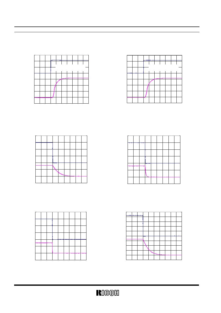
12) Turn-on speed with CE pin
R1131x08xx
R1131x08xx
V
IN
=1.8V C
IN
= Tantalum 1.0
µ
F V
IN
=1.8V, C
IN
= Tantalum 1.0
µ
F
C
OUT
= Tantalum 1.0uF, I
OUT
=0mA C
OUT
= Tantalum 1.0uF, I
OUT
=30mA
-2.7
-1.8
-0.9
0
0.9
1.8
2.7
-30 -20 -10
0
10 20 30 40 50 60 70
Time t[
µ
s]
CE I
nput
Vol
t
age V
CE
[V
]
-0.5
0
0.5
1
1.5
2
2.5
Out
put
Vol
t
age V
OU
T
[V
]
-2.7
-1.8
-0.9
0
0.9
1.8
2.7
-30 -20 -10
0
10 20 30 40 50 60 70
Time t[
µ
s]
CE Input Voltage V
CE
[V]
-0.5
0
0.5
1
1.5
2
2.5
Output Voltage V
OU
T
[V]
R1131x08xx
R1131x33xx
V
IN
=1.8V C
IN
= Tantalum 1.0
µ
F V
IN
=4.3V, C
IN
= Ceramic 1.0
µ
F
C
OUT
= Tantalum 1.0uF, I
OUT
=300mA C
OUT
= Ceramic 1.0uF, I
OUT
=0mA
-2.7
-1.8
-0.9
0
0.9
1.8
2.7
-30 -20 -10 0
10 20 30 40 50 60 70
Time t[
µ
s]
CE I
nput
Vol
t
age V
CE
[V
]
-0.5
0
0.5
1
1.5
2
2.5
Out
put
Vol
t
age V
OU
T
[V
]
-10
-8
-6
-4
-2
0
2
4
6
-60 -40 -20
0
20 40 60 80 100 120 140
Time t[
µ
s]
C
E
Input V
o
ltage V
CE
[V
]
-1
0
1
2
3
4
5
6
7
Output V
o
ltage V
OU
T
[V
]
VCE=0V
1.8V
VCE=0V
1.8V
Load
C
Load
C
Output Voltage
Output Voltage
R1131x
17
R1131x33xx
R1131x33xx
V
IN
=4.3V C
IN
= Ceramic 1.0
µ
F V
IN
=4.3V, C
IN
= Ceramic 1.0
µ
F
C
OUT
= Ceramic 1.0
µ
F, I
OUT
=30mA C
OUT
= Ceramic 1.0
µ
F, I
OUT
=300mA
-10
-8
-6
-4
-2
0
2
4
6
-60 -40 -20
0
20
40
60
80 100 120 140
Time t[
µ
s]
CE Input Voltage V
CE
[V]
-1
0
1
2
3
4
5
6
7
Output Voltage V
OU
T
[V]
-10
-8
-6
-4
-2
0
2
4
6
-60 -40 -20
0
20
40
60
80 100 120 140
Time t[
µ
s]
CE I
nput
Vol
t
age V
CE
[V
]
-1
0
1
2
3
4
5
6
7
O
u
t
put
Vol
t
age V
OU
T
[V
]
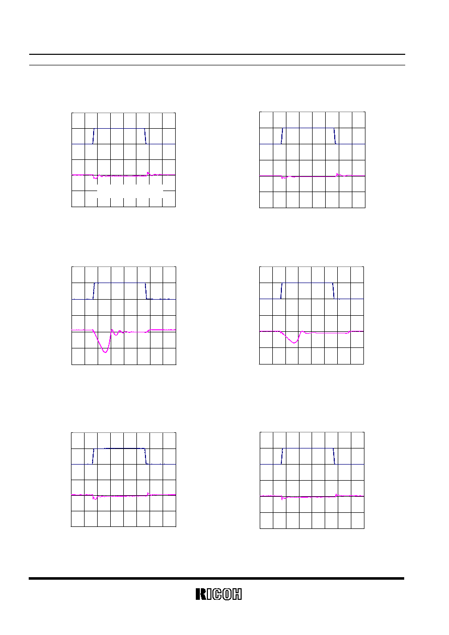
13) Turn-off speed with CE pin
R1131x08xD
R1131x08xD
V
IN
=1.8V C
IN
= Tantalum 1.0
µ
F V
IN
=1.8V, C
IN
= Tantalum 1.0
µ
F
C
OUT
= Tantalum 1.0
µ
F, I
OUT
=0mA C
OUT
= Tantalum 1.0
µ
F, I
OUT
=30mA
-1.8
-1.2
-0.6
0
0.6
1.2
1.8
2.4
-0.6 -0.4 -0.2
0
0.2 0.4 0.6 0.8
1
1.2
Time t[ms]
CE Input Voltage V
CE
[V]
-0.5
0
0.5
1
1.5
2
2.5
3
Output Voltage V
OU
T
[V]
-1.8
-1.2
-0.6
0
0.6
1.2
1.8
2.4
-0.6 -0.4 -0.2
0
0.2 0.4 0.6 0.8
1
1.2
Time t[ms]
CE I
nput
Vol
t
age V
CE
[V
]
-0.5
0
0.5
1
1.5
2
2.5
3
O
u
t
put
Vol
t
age V
OU
T
[V
]
R1131x08xD
R1131x33xD
V
IN
=1.8V C
IN
= Tantalum 1.0
µ
F V
IN
=4.3V, C
IN
= Ceramic 1.0
µ
F
C
OUT
= Tantalum 1.0
µ
F, I
OUT
=300mA C
OUT
= Ceramic 1.0
µ
F, I
OUT
=0mA
-1.8
-1.2
-0.6
0
0.6
1.2
1.8
2.4
-0.6 -0.4 -0.2
0
0.2 0.4 0.6 0.8
1
1.2
Time t[ms]
CE I
nput
Vol
t
age V
CE
[V
]
-0.5
0
0.5
1
1.5
2
2.5
3
O
u
t
put
Vol
t
age V
OU
T
[V
]
-5
-4
-3
-2
-1
0
1
2
3
4
5
-0.3 -0.2 -0.1
0
0.1 0.2 0.3 0.4 0.5 0.6 0.7
Time t[ms]
CE I
nput
Vol
t
age V
CE
[V
]
-1
0
1
2
3
4
5
6
7
8
9
O
u
t
put
Vol
t
age V
OU
T
[V
]
VCE=0V
4.3V
VCE=0V
4.3V

R1131x
18
R1131x33xD
R1131x33xD
V
IN
=4.3V C
IN
= Ceramic 1.0
µ
F V
IN
=4.3V, C
IN
= Ceramic 1.0
µ
F
C
OUT
= Ceramic 1.0
µ
F, I
OUT
=30mA C
OUT
= Ceramic 1.0
µ
F, I
OUT
=300mA
-5
-4
-3
-2
-1
0
1
2
3
4
5
-0.3 -0.2 -0.1 0 0.1 0.2 0.3 0.4 0.5 0.6 0.7
Time t[ms]
C
E
I
nput
Volt
age V
CE
[V
]
-1
0
1
2
3
4
5
6
7
8
9
Out
put
Volt
age V
OU
T
[V
]
-5
-4
-3
-2
-1
0
1
2
3
4
5
-0.3 -0.2 -0.1 0 0.1 0.2 0.3 0.4 0.5 0.6 0.7
Time t[ms]
C
E
Input Vol
t
age V
CE
[V]
-1
0
1
2
3
4
5
6
7
8
9
Output Vol
t
age V
OU
T
[V]
TECHNICAL NOTES
When using these ICs, consider the following points:
In these ICs, phase compensation is made for securing stable operation even if the load current is varied. For this
purpose, use a capacitor C
OUT
with good frequency characteristics and ESR (Equivalent Series Resistance) of which is in
the range described as follows:
The relations between I
OUT
(Output Current) and ESR of an output capacitor are shown below. The conditions when the
white noise level is under 40
µ
V (Avg.) are marked as the hatched area in the graph.
<Test conditions>
(1) Frequency Band: 10Hz to 2MHz
(2) Temperature:
25∞
C
R1131x08xx
R1131x10xx
V
IN
=1.4V to 6.0V
V
IN
=1.4V to 6.0V
C
IN
= Ceramic 1.0
µ
F,C
OUT
= Ceramic 1.0
µ
F
C
IN
= Ceramic 1.0
µ
F,C
OUT
= Ceramic 1.0
µ
F
0.01
0.1
1
10
100
0
50
100
150
200
250
300
Output Current IOUT [mA]
ESR [
]
0.01
0.1
1
10
100
0
100
200
300
Output Current IOUT [mA ]
ESR [
O
hm
]

R1131x
19
R1131x26xx
R1131x15xx
V
IN
=3.0V to 6.0V
V
IN
=2.0V to 6.0V
C
IN
= Ceramic 1.0
µ
F,C
OUT
= Ceramic 1.0
µ
F C
IN
= Ceramic 1.0
µ
F,C
OUT
= Ceramic 1.0
µ
F
0.01
0.1
1
10
100
0
100
200
300
Output Current I
OUT
[mA ]
ESR [
]
0.01
0.1
1
10
100
0
100
200
300
Output Current I
OUT
[mA]
ESR
[
]