 | –≠–ª–µ–∫—Ç—Ä–æ–Ω–Ω—ã–π –∫–æ–º–ø–æ–Ω–µ–Ω—Ç: R1150H | –°–∫–∞—á–∞—Ç—å:  PDF PDF  ZIP ZIP |

R1150H SERIES
VOLTAGE REGULATOR(with Wide Input Voltage Range) with RESET
NO.EA-081-0610
1
OUTLINE
The R1150H series are CMOS-based voltage regulator (VR) ICs equipped with a voltage detector (V
DET
). VR
function of the R1150Hxxxx has features of low dropout voltage, high output voltage accuracy, and ultra-low
supply current. Each of the R1150HxxxA types includes also a chip enable circuit. The output of built-in voltage
detector is Nch open drain type. The R1150HxxxC/D types have a pin for connecting external capacitor to set a
certain reset delay time instead of chip enable control pin.
The regulator output voltage and the detector threshold voltage are fixed in the IC, Output Voltage Accuracy is
±2.0%, while Detector Threshold Accuracy is ±2.5%. The R1150HxxxA (with chip enable function) and C series
can supervise input voltage by the built-in detector. R1150HxxxB type can supervise SENSE pin voltage by the
built-in detector. R1150HxxxD type can supervise V
OUT
voltage, or Regulator Output Voltage of this IC itself.
Since the package for these ICs is the SOT-89-5 package, high density mounting of the ICs on boards is
possible.
FEATURES
∑ Ultra-Low Supply Current..................................................... Typ. 7.0µA
∑ Input Voltage ........................................................................ Max. 24.0V
∑ Output Voltage (VR)............................................................. 2.1V to 14.0V
∑ Detector Threshold Voltage (V
DET
) ....................................... 2.3V to 15.0V
∑ High Output Voltage Accuracy ............................................. ±2.0% (VR), ±2.5% (VD)
∑ Output Current ..................................................................... Min. 150mA (V
OUT
=5.0V)
∑ Small Package ..................................................................... SOT-89-5
∑ Built-in Current Limit Circuit, Thermal Shutdown Circuit (VR)
∑ Monitoring V
DD
voltage ......................................................... A/C type
∑ Monitoring sense pin (SENSE) voltage ................................B type
∑ Monitoring V
OUT
pin voltage.................................................. D type
APPLICATIONS
∑ Power source and Reset circuit for cameras, videos and mobile telecommunication equipment.
∑ Power source and Reset circuit for battery-operated equipment.
∑ Power source and Reset circuit for home appliances.

R1150H
2
BLOCK DIAGRAMS
R1150HxxxA
R1150HxxxB
5
2
4
3
V
OUT
V
DET
CE
V
DD
GND
Detector
1
Chip Enable
Thermal
Shutdown
Regulator
5
2
4
3
V
OUT
V
DET
SENSE
V
DD
GND
Detector
1
Thermal
Shutdown
Regulator
R1150HxxxC
R1150HxxxD
5
2
4
3
V
OUT
V
DET
CD
V
DD
GND
Detector
1
Delay
Thermal
Shutdown
Regulator
5
2
4
3
V
OUT
V
DET
CD
V
DD
GND
Detector
1
Delay
Thermal
Shutdown
Regulator
SELECTION GUIDE
The output voltage and the usage of pin No.3 (as a kind of types in the R1150Hxxxx series) can be selected at
the user's request. The selection can be made with designating the part number as follows;
R1150Hxxxx-T1-x
Part Number
a b c d e
Code Contents
a
Designation of package type;
H: SOT-89-5
b
Serial Number for Voltage Setting
c
Designation of option;
A: Built-in Chip Enable Circuit (V
DET
supervises V
IN
level.)
B: V
DET
supervises SENSE pin.
C: Used with an external capacitor for setting output delay time of V
DET
. (V
DET
supervises V
IN
.)
D: Used with an external capacitor for setting output delay time of V
DET
. (V
DET
supervises V
OUT
.)
d
Designation of Taping Type; (Refer to Taping Specifications)
e
Designation of composition of pin plating:
-F: Lead free plating
R1150H
3
PIN CONFIGURATION
SOT-89-5
5
4
1
2
3
PIN DESCRIPTION
Pin No.
Symbol
Description
1 V
OUT
Voltage Regulator Output Pin
2 GND
Ground
Pin
CE (A type)
Chip Enable Pin
SENSE (B type) Sense Pin for Voltage Detector
3
CD (C/D type)
Pin for External Capacitor for Setting Output Delay
of Voltage Detector
4 V
DET
Voltage Detector Output Pin
5 V
DD
Input
Pin
ABSOLUTE MAXIMUM RATINGS
Symbol Item
Rating
Unit
V
IN
Input
Voltage
26.0
V
V
CE
Input Voltage (CE Input Pin)*
Note1
-0.3 ~ V
IN
+0.3 V
V
SENSE
Input Voltage (SENSE Input Pin)*
Note2
-0.3 ~ V
IN
+0.3 V
V
CD
Input Voltage (CD Input Pin)*
Note3
-0.3 ~ V
IN
+0.3
V
V
DED
Output Voltage (V
DET
Output Pin)
-0.3 ~ V
IN
+0.3
V
V
OUT
Output Voltage
-0.3 ~ V
IN
+0.3
V
I
OUT1
Output Current (VR)
250
mA
I
OUT2
Output Current (VD)
10
mA
P
D
Power Dissipation (SOT-89-5)*
1
500
mW
Topt Operating
Temperature
-40
~
85
∞C
Tstg Storage
Temperature
-55
~
125
∞C
*Note1: This item is for A Version.
*Note2: This item is for B Version
*Note3: This item is for C/D Version
1
For Power Dissipation, please refer to PACKAGE INFORMATION to be described.
R1150H
4
ELECTRICAL CHARACTERISTICS
∑
R1150HxxxA
Topt
=25∞C
Symbol Item
Conditions Min.
Typ.
Max.
Unit
V
IN
Input
Voltage
24.0
V
I
SS1
Supply Current 1
V
IN
=V
CE
V
OUT
(-V
DET
):V
IN
-V
OUT
=2.0V
V
OUT
<(-V
DET
):V
IN
=(-V
DET
)+2.0V
7
14
µA
I
SS2
Supply Current 2
V
DD
=24V, V
CE
=0V
Refer to Supply Current 2 Table
T
SD
Thermal Shutdown
Temperature
Junction Temperature
150
T
SR
Thermal Shutdown
Released Temperature
Junction Temperature
120
VR part
Topt
=25∞C
Symbol Item
Conditions Min.
Typ.
Max.
Unit
V
OUT
Output
voltage
V
IN
-V
OUT
=2.0V,I
OUT
=20mA
◊
0.98
◊
1.02
V
I
OUT
Output
Current
V
IN
-V
OUT
=2.0V
Refer to Output Current Table
V
OUT
/
I
OUT
Load Regulation
V
IN
-V
OUT
=2.0V
1mA
<
=
I
OUT
<
=
40mA
Refer to Load Regulation Table
V
OUT
/
V
IN
Line Regulation
V
IN
-V
OUT
=2.0V,I
OUT
=20 mA
V
OUT
+1V
<
=
V
IN
<
=
24V
0.05
0.15
%/V
V
DIF
Dropout
Voltage
I
OUT
=20mA
Refer to Dropout Voltage Table
V
OUT
/
Topt
Output Voltage
Temperature Coefficient
V
IN
-V
OUT
=2.0V,I
OUT
=20mA
-40∞C
<
=
Topt
<
=
85∞C
±100
ppm/∞C
I
lim
Short Current Limit
V
OUT
=0V
45
mA
V
CEH
CE "H" Input Voltage
1.5
V
IN
V
V
CEL
CE "L" Input Voltage
0.00
0.25
V
V
DET
part
Topt
=25∞C
Symbol Item
Conditions Min.
Typ.
Max.
Unit
-V
DET
Detector
Threshold
◊
0.975
◊
1.025
V
V
HYS
Detector Threshold
Hysteresis
-V
DET
◊
0.03
-V
DET
◊
0.05
-V
DET
◊
0.07
V
I
DOUT
Sink
Current
V
IN
=2.0V, V
DET
=0.05V 0.15
0.20
µA
V
DDL
Minimum Operating
Voltage
*Note 1
0.9
1.2
V
-V
DET
/
Topt
Detector Threshold
Temperature Coefficient
-40∞C
<
=
Topt
<
=
85∞C
±100
ppm/∞C
t
PLH
Output Delay Time
*Note 2
0.5
1.0
ms

R1150H
5
∑
R1150HxxxB
Topt
=25∞C
Symbol Item
Conditions Min.
Typ.
Max.
Unit
V
IN
Input
Voltage
24.0
V
I
SS
Supply
Current
V
OUT
(-V
DET
):
V
IN
=SENSE=V
OUT
+2.0V
V
OUT
< (-V
DET
):
V
IN
=SENSE=(-V
DET
)+2.0V
7
14
µA
T
SD
Thermal Shutdown
Temperature
Junction Temperature
150
∞C
T
SR
Thermal Shutdown
Temperature
Junction Temperature
120
∞C
VR part
Topt
=25∞C
Symbol Item
Conditions Min.
Typ.
Max.
Unit
V
OUT
Output
voltage
V
IN
-V
OUT
=2.0V
I
OUT
=20mA
V
SET
◊
0.98
V
SET
V
SET
◊
1.02
V
I
OUT
Output
Current
V
IN
-V
OUT
=2.0V
Refer to Output Current Table
V
OUT
/
I
OUT
Load Regulation
V
IN
-V
OUT
=2.0V
1mA
<
=
I
OUT
<
=
40mA
Refer to Load Regulation Table
V
OUT
/
V
IN
Line Regulation
I
OUT
=20mA
V
OUT
+1V
<
=
V
IN
<
=
24V
0.05
0.15
%/V
V
DIF
Dropout
Voltage
I
OUT
=20mA
Refer to Dropout Voltage Table
V
OUT
/
Topt
Output Voltage
Temperature Coefficient
V
IN
-V
OUT
=2.0V
I
OUT
=20mA
-40∞C
<
=
Topt
<
=
85∞C
±100
ppm/∞C
I
lim
Short Current Limit
V
OUT
=0V
45
mA
V
DET
part
Topt
=25∞C
Symbol Item
Conditions
Min.
Typ.
Max.
Unit
-V
DET
Detector
Threshold
V
SET
◊
0.975
V
SET
V
SET
◊
1.025
V
V
HYS
Detector Threshold
Hysteresis
-V
DET
◊
0.03
-V
DET
◊
0.05
-V
DET
◊
0.07
V
I
DOUT
Sink
Current
V
IN
=SENSE=2.0V, V
DS
=0.05V 0.17
mA
V
DDL
Minimum Operating Voltage *Note 1
0.9
1.2
V
-V
DET
/
Topt
Detector Threshold
Temperature Coefficient
-40∞C
<
=
Topt
<
=
85∞C
±100
ppm/∞C
t
PLH
Output Delay Time
*Note 2
1.0
1.5
ms

R1150H
6
∑
R1150HxxxC
Topt
=25∞C
Symbol Item
Conditions Min.
Typ.
Max.
Unit
V
IN
Input
Voltage
24.0
V
I
SS1
Supply
Current
V
OUT
(-V
DET
):V
IN
= V
OUT
+2.0V
V
OUT
< (-V
DET
):V
IN
= (-V
DET
)+2.0V
7
14
µA
T
SD
Thermal Shutdown
Temperature
Junction Temperature
150
∞C
T
SR
Thermal Shutdown
Released Temperature
Junction Temperature
120
∞C
VR part
Topt
=25∞C
Symbol Item
Conditions Min.
Typ.
Max.
Unit
V
OUT
Output
voltage
V
IN
-V
OUT
=2.0V
I
OUT
=20mA
V
SET
◊
0.98
V
SET
V
SET
◊
1.02
V
I
OUT
Output
Current
V
IN
-V
OUT
=2.0V
Refer to Output Current Table
V
OUT
/
I
OUT
Load Regulation
V
IN
-V
OUT
=2.0V
1mA
<
=
I
OUT
<
=
40mA
Refer to Load Regulation Table
V
OUT
/
V
IN
Line Regulation
I
OUT
=20mA
V
OUT
+1V
<
=
V
IN
<
=
24V
0.05
0.15
%/V
V
DIF
Dropout
Voltage
I
OUT
=20mA
Refer to Dropout Voltage Table
V
OUT
/
Topt
Output Voltage
Temperature Coefficient
V
IN
-V
OUT
=2.0V
I
OUT
=20mA
-40∞C
<
=
Topt
<
=
85∞C
±100
ppm/∞C
I
lim
Short Current Limit
V
OUT
=0V
45
mA
V
DET
part
Topt
=25∞C
Symbol Item
Conditions
Min.
Typ.
Max.
Unit
-V
DET
Detector
Threshold
V
SET
◊
0.975
V
SET
V
SET
◊
1.025
V
V
HYS
Detector Threshold
Hysteresis
-V
DET
◊
0.03
-V
DET
◊
0.05
-V
DET
◊
0.07
V
I
DOUT
Sink
Current
V
IN
=2.0V, V
DS
=0.05V 0.17
mA
V
DDL
Minimum Operating Voltage *Note 1
0.9
1.2
V
-V
DET
/
Topt
Detector Threshold
Temperature Coefficient
-40∞C
<
=
Topt
<
=
85∞C
±100
ppm/∞C
t
PLH
Output Delay Time
Cd=4.7nF, *Note 2
20
30
50
ms
R1150H
7
∑
R1150HxxxD
Topt
=25∞C
Symbol Item
Conditions Min.
Typ.
Max.
Unit
V
IN
Input
Voltage
24.0
V
I
SS
Supply
Current
V
IN
-V
OUT
=2.0V
7
14
µA
T
SD
Thermal Shutdown
Temperature
150
∞C
T
SR
Thermal Shutdown
Released Temperature
Junction Temperature
120
∞C
VR part
Topt
=25∞C
Symbol Item
Conditions Min.
Typ.
Max.
Unit
V
OUT
Output
Voltage
V
IN
-V
OUT
=2.0V
I
OUT
=20mA
V
SET
◊
0.98
V
SET
V
SET
◊
1.02
V
I
OUT
Output
Current
V
IN
-V
OUT
=2.0V
Refer to Output Current Table
V
OUT
/
I
OUT
Load Regulation
V
IN
-V
OUT
=2.0V
1mA
<
=
I
OUT
<
=
40mA
Refer to Load Regulation Table
V
OUT
/
V
IN
Line Regulation
I
OUT
=20mA
V
OUT
+1V
<
=
V
IN
<
=
24V
0.05
0.15
%/V
V
OUT
/
Topt
Output Voltage
Temperature Coefficient
V
IN
-V
OUT
=2.0V
I
OUT
=20mA
-40∞C
<
=
Topt
<
=
85∞C
±100
ppm/∞C
I
lim
Short Current Limit
V
OUT
=0V
45
mA
V
DET
part
Topt
=25∞C
Symbol Item
Conditions
Min.
Typ.
Max.
Unit
-V
DET
Detector
Threshold
V
SET
◊
0.975
V
SET
V
SET
◊
1.025
V
V
HYS
Detector Threshold
Hysteresis
-V
DET
◊
0.03
-V
DET
◊
0.05
-V
DET
◊
0.07
V
I
DOUT
Sink
Current
V
IN
=2.0V, V
DS
=0.05V 0.17
mA
V
DDL
Minimum Operating
Voltage
*Note 1
0.9
1.2
V
-V
DET
/
Topt
Detector Threshold
Temperature Coefficient
-40∞C
<
=
Topt
<
=
85∞C
±100
ppm/∞C
t
PD
Output Delay Time
Cd=4.7nF, *Note 2
20
30
50
ms
Release
Margin
V
OUT
-0.2-(-V
DET
)-V
HYS
50
mV
Note 1) This item means V
DD
Voltage when Output Voltage is equal or less than 0.1V
(Pull-up Resistor=470k
, Pull up Voltage=5V
Note 2) V
DET
pin is pulled up to V
DD
via 470k
. tpLH means time interval from rising edge of V
DD
from
(-V
DET
)-2.0V to (-V
DET
)+2.0V to the point of Output Voltage being 80% of pull-up voltage.

R1150H
8
∑
Output Current (Topt=25∞C)
Output Current (mA)
Output Voltage V
OUT
(V)
Min.
2.1V
<
=
V
OUT
<
=
2.9V
90
3.0V
<
=
V
OUT
<
=
4.0V
120
4.1V
<
=
V
OUT
<
=
14.0V
150
∑
Load Regulation (Topt=25∞C)
Load Regulation (mV)
Output Voltage V
OUT
(V)
Typ.
Max.
2.1V
<
=
V
OUT
<
=
3.0V
15
35
3.1V
<
=
V
OUT
<
=
5.0V
25
45
5.1V
<
=
V
OUT
<
=
10.0V
40
65
10.1V
<
=
V
OUT
<
=
14.0V 50 80
∑
Dropout Voltage (Topt=25∞C)
Dropout Voltage (V)
Output Voltage V
OUT
(V)
Typ.
Max.
2.1V
<
=
V
OUT
<
=
2.4V
0.40 0.60
2.5V
<
=
V
OUT
<
=
3.0V
0.30 0.40
3.1V
<
=
V
OUT
<
=
7.0V
0.25 0.35
7.1V
<
=
V
OUT
<
=
10.0V
0.27 0.45
10.1V
<
=
V
OUT
<
=
14.0V
0.30 0.50
∑
Supply Current 2 (Off state with CE) (Topt=25∞C)
Supply Current (µA)
Detector Threshold Voltage
-V
DET
(V)
Typ.
Max.
2.3V
<
=
V
OUT
<
=
3.0V
2.5 5.0
3.1V
<
=
V
OUT
<
=
15.0V
3.0 6.0

R1150H
9
TEST CIRCUITS
∑
R1150HxxxA
5
1
2
3
CE
V
OUT
GND
R1150HxxxA
SERIES
C
IN
=0.1
µ
F, C
OUT
=1
µ
F
C
IN
V
IN
C
OUT
I
OUT
470k
V
DD
4
V
DET
5
1
2
3
CE
V
OUT
GND
R1150HxxxA
SERIES
C
IN
=0.1
µ
F, C
OUT
=1
µ
F
C
IN
V
IN
C
OUT
V
DD
4
V
DET
Standard Test Circuit
Supply Current Test Circuit
5
1
2
3
CE
V
OUT
GND
R1150HxxxA
SERIES
C
IN
=0.1
µ
F, C
OUT
=1
µ
F
V
IN
C
OUT
I
OUT
V
DD
4
V
DET
P.G.
5
1
2
3
CE
V
OUT
GND
R1150HxxxA
SERIES
C
IN
=0.1
µ
F, C
OUT
=1
µ
F
C
IN
V
IN
C
OUT
I
OUT
V
DD
4
V
DET
I1
I2
Input Transient Response/
Load Transient Response Test Circuit
Ripple Rejection Test Circuit
5
1
2
3
CE
V
OUT
GND
R1150HxxxA
SERIES
C
IN
=0.1
µ
F
C
IN
V
IN
V
DD
4
V
DET
470k
5V
5
1
2
3
CE
V
OUT
GND
R1150HxxxA
SERIES
C
IN
=0.1
µ
F
C
IN
2V
V
DD
4
V
DET
0.05V
Minimum Operating Voltage Test Circuit
V
DET
Output Current Test Circuit

R1150H
10
∑
R1150HxxxB
5
1
2
3
SENSE
V
OUT
GND
R1150HxxxB
SERIES
C
IN
=0.1
µ
F, C
OUT
=1
µ
F
C
IN
V
IN2
C
OUT
I
OUT
470k
V
DD
4
V
DET
V
IN1
5
1
2
3
GND
R1150HxxxB
SERIES
C
IN
=0.1
µ
F, C
OUT
=1
µ
F
C
IN
V
IN2
C
OUT
4
V
IN1
SENSE
V
OUT
V
DD
V
DET
Standard Test Circuit
Supply Current Test Circuit
5
1
2
3
SENSE
V
OUT
GND
R1150HxxxB
SERIES
C
IN
=0.1
µ
F, C
OUT
=1
µ
F
V
IN1
C
OUT
I
OUT
V
DD
4
V
DET
P.G.
V
IN2
5
1
2
3
SENSE
V
OUT
GND
R1150HxxxB
SERIES
C
IN
=0.1
µ
F, C
OUT
=1
µ
F
C
OUT
I
OUT
V
DD
4
V
DET
I
1
I
2
C
IN
V
IN2
V
IN1
Input Transient Response/
Load Transient Response Test Circuit
Ripple Rejection Test Circuit
5
1
2
3
SENSE
V
OUT
GND
R1150HxxxB
SERIES
C
IN
=0.1
µ
F
C
IN
V
IN
V
DD
4
V
DET
470k
5V
5
1
2
3
SENSE
V
OUT
GND
R1150HxxxB
SERIES
C
IN
=0.1
µ
F
C
IN
2V
V
DD
4
V
DET
0.05V
V
DET
Minimum Operating Voltage Test Circuit
V
DET
Output Current Test Circuit

R1150H
11
∑
R1150HxxxC/D
5
1
2
3
CD
V
OUT
GND
R1150HxxxC/D
SERIES
C
IN
=0.1
µ
F, C
OUT
=1
µ
F
C
IN
C
D
C
OUT
I
OUT
470k
V
DD
4
V
DET
V
IN
5
1
2
3
GND
R1150HxxxC/D
SERIES
C
IN
=0.1
µ
F, C
OUT
=1
µ
F
C
IN
C
OUT
4
V
IN
CD
V
OUT
V
DD
V
DET
Standard Test Circuit
Supply Current Test Circuit
5
1
2
3
CD
V
OUT
GND
R1150HxxxC/D
SERIES
C
IN
=0.1
µ
F, C
OUT
=1
µ
F
V
IN
C
OUT
I
OUT
V
DD
4
V
DET
P.G.
C
D
5
1
2
3
CD
V
OUT
GND
R1150HxxxC/D
SERIES
C
IN
=0.1
µ
F, C
OUT
=1
µ
F
C
OUT
I
OUT
V
DD
4
V
DET
I
1
I
2
V
IN
C
IN
Input Transient Response/
Load Transient Response Test Circuit
Ripple Rejection Test Circuit
5
1
2
3
CD
V
OUT
GND
R1150HxxxC/D
SERIES
C
IN
=0.1
µ
F
C
IN
V
IN
V
DD
4
V
DET
470k
5V
C
D
5
1
2
3
CD
V
OUT
GND
R1150HxxxC/D
SERIES
C
IN
=0.1
µ
F
C
IN
2V
V
DD
4
V
DET
0.05V
C
D
V
DET
Minimum Operating Voltage Test Circuit
V
DET
Output Current Test Circuit

R1150H
12
TYPICAL CHARACTERISTICS
1) Output Voltage vs. Temperature
R1150H (VR=3.0V)
R1150H (VR=5.0V)
3.06
3.03
3.00
2.97
2.94
Temperature Topt(
∞
C)
Output Voltage V
OUT
(V)
-50
0
50
100
5.10
5.05
5.00
4.95
4.90
-50
0
50
100
Temperature Topt(
∞
C)
Output Voltage V
OUT
(V)
R1150H
(VR=10.0V)
10.2
10.1
10.0
9.9
9.8
-50
0
50
100
Temperature Topt(
∞
C)
Output Voltage V
OUT
(V)
2) Input Voltage vs. Output Voltage
R1150H (VR=3.0V)
R1150H (VR=5.0V)
4.0
3.5
3.0
2.5
2.0
0
5
10
15
20
25
Topt=25
∞
C
I
OUT
=1mA
I
OUT
=20mA
I
OUT
=40mA
Input Voltage V
IN
(V)
Output Voltage V
OUT
(V)
6.0
5.5
5.0
4.5
4.0
0
5
10
15
20
25
Topt=25
∞
C
I
OUT
=1mA
I
OUT
=20mA
I
OUT
=40mA
Input Voltage V
IN
(V)
Output Voltage V
OUT
(V)
R1150H
13
R1150H
(VR=10.0V)
11.0
10.5
10.0
9.5
9.0
0
5
10
15
20
25
Topt=25
∞
C
I
OUT
=1mA
I
OUT
=20mA
I
OUT
=40mA
Input Voltage V
IN
(V)
Output Voltage V
OUT
(V)
3) Output Voltage vs. Output Current
R1150H (VR=3.0V)
R1150H (VR=5.0V)
3.5
2.5
1.5
3.0
2.0
1.0
0.5
0.0
0
100
200
300
Topt=25
∞
C
V
IN
=4V
V
IN
=5V
Output Current I
OUT
(mA)
Output Voltage V
OUT
(V)
6.0
5.0
3.0
4.0
2.0
1.0
0.0
0
100
200
300
Topt=25
∞
C
Output Current I
OUT
(mA)
Output Voltage V
OUT
(V)
V
IN
=6V
V
IN
=7V
R1150H
(VR=10.0V)
12
10
6
8
4
2
0
0
100
200
300
Topt=25
∞
C
V
IN
=11V
V
IN
=12V
Output Current I
OUT
(mA)
Output Voltage V
OUT
(V)

R1150H
14
4) Dropout Voltage vs. Output Current
R1150H (VR=3.0V)
R1150H (VR=5.0V)
3.0
2.5
1.5
2.0
1.0
0.5
0.0
0
30
60
120
90
85
∞
C
25
∞
C
-40
∞
C
Output Current I
OUT
(mA)
Dropout Voltage V
DIF
(V)
3.0
2.5
1.5
2.0
1.0
0.5
0.0
0
30
60
150
120
90
85
∞
C
25
∞
C
-40
∞
C
Output Current I
OUT
(mA)
Dropout Voltage V
DIF
(V)
R1150H
(VR=10.0V)
3.0
2.5
1.5
2.0
1.0
0.5
0.0
0
30
60
150
120
90
85
∞
C
25
∞
C
-40
∞
C
Output Current I
OUT
(mA)
Dropout Voltage V
DIF
(V)
5) Supply Current vs. Input Voltage
R1150H (VR=3.0V)
R1150H (VR=5.0V)
10
6
8
4
2
0
0
10
20
5
15
25
Topt=25
∞
C
Input Voltage V
IN
(V)
Supply Current I
SS
(
µ
A)
10
6
8
4
2
0
0
10
20
5
15
25
Topt=25
∞
C
Input Voltage V
IN
(V)
Supply Current I
SS
(
µ
A)

R1150H
15
R1150H
(VR=10.0V)
10
6
8
4
2
0
0
10
20
5
15
25
Topt=25
∞
C
Input Voltage V
IN
(V)
Supply Current I
SS
(
µ
A)
6) Supply Current vs. Temperature
R1150H (VR=3.0V, V
DET
=2.5V)
R1150H (VR=5.0V, V
DET
=4.5V)
10
6
8
4
2
0
Temperature Topt(
∞
C)
-50
0
50
100
Supply Current I
SS
(
µ
A)
10
6
8
4
2
0
-50
0
50
100
Temperature Topt(
∞
C)
Supply Current I
SS
(
µ
A)
R1150H (VR=10.0V, V
DET
=11.0V)
10
6
8
4
2
0
-50
0
50
100
Temperature Topt(
∞
C)
Supply Current I
SS
(
µ
A)

R1150H
16
7) Ripple Rejection vs. Frequency
R1150H (VR=3.0V)
R1150H (VR=5.0V)
80
40
60
20
70
30
50
10
0
Frequency f(kHz)
0.01
1
0.1
10
100
V
IN
=5.0V
DC
+0.5Vp-p, I
OUT
=20mA, C
OUT
=1
µ
F
Topt=25
∞
C
Ripple Rejection RR(dB)
80
40
60
20
70
30
50
10
0
0.01
1
0.1
10
100
V
IN
=7.0V
DC
+0.5Vp-p, I
OUT
=20mA, C
OUT
=1
µ
F
Topt=25
∞
C
Frequency f(kHz)
Ripple Rejection RR(dB)
R1150H
(VR=10.0V)
80
40
60
20
70
30
50
10
0
0.01
1
0.1
10
100
V
IN
=12.0V
DC
+0.5Vp-p, I
OUT
=20mA, C
OUT
=1
µ
F
Topt=25
∞
C
Frequency f(kHz)
Ripple Rejection RR(dB)

R1150H
17
8) Input
Transient
Response
R1150H (VR=3.0V)
I
OUT
=20mA, C
OUT
=1
µ
F
3.4
3.3
3.2
3.1
3.0
2.9
2.8
20
15
10
5
0
-5
-10
Time T(ms)
Input Voltage V
IN
(V)
40
0
80
160
200
120
Output Voltage V
OUT
(V)
Output Voltage
Input Voltage
R1150H (VR=5.0V)
I
OUT
=20mA, C
OUT
=1
µ
F
5.4
5.3
5.2
5.1
5.0
4.9
4.8
20
15
10
5
0
-5
-10
Time T(ms)
Input Voltage V
IN
(V)
40
0
80
160
200
120
Output Voltage V
OUT
(V)
Input Voltage
Output Voltage
R1150H (VR=10.0V)
I
OUT
=20mA, C
OUT
=1
µ
F
11.0
10.6
10.8
10.4
10.2
10.0
9.8
9.6
25
20
15
10
5
0
-5
-10
Time T(ms)
Input Voltage V
IN
(V)
40
0
80
160
200
120
Output Voltage V
OUT
(V)
Input Voltage
Output Voltage

R1150H
18
9) Load
Transient
Response
R1150H (VR=3.0V)
V
IN
=5.0V, C
OUT
=1
µ
F
5.5
4.5
5.0
4.0
3.5
3.0
2.5
30
20
10
0
-10
-20
-30
Time T(ms)
Output Voltage I
OUT
(mA)
5
-5
15
30
25
0
10
20
Output Voltage V
OUT
(V)
Topt=25
∞
C
1mA
20mA
Output Voltage
Output Current
R1150H (VR=5.0V)
V
IN
=7.0V, C
OUT
=1
µ
F
7.0
6.2
6.6
5.8
5.4
5.0
4.6
30
20
10
0
-10
-20
-30
5
-5
15
30
25
0
10
20
Topt=25
∞
C
1mA
20mA
Time T(ms)
Output Voltage I
OUT
(mA)
Output Voltage V
OUT
(V)
Output Voltage
Output Current
R1150H (VR=10.0V)
V
IN
=12.0V, C
OUT
=1
µ
F
12.5
11.5
12.0
11.0
10.5
10.0
9.5
30
20
10
0
-10
-20
-30
5
-5
15
30
25
0
10
20
Topt=25
∞
C
1mA
20mA
Time T(ms)
Output Voltage I
OUT
(mA)
Output Voltage V
OUT
(V)
Output Voltage
Output Current
R1150H
19
10) Detector Threshold vs. Temperature
R1150H
(-V
DET
=4.5V) R1150H
(-V
DET
=11.0V)
4.8
4.7
4.6
4.5
4.4
Temperature Topt(
∞
C)
Input Voltage V
IN
(V)
-50
0
50
100
+V
DET
-V
DET
11.8
11.6
11.2
11.4
11.0
10.8
-50
0
50
100
+V
DET
-V
DET
Temperature Topt(
∞
C)
Input Voltage V
IN
(V)
11) Detector Threshold vs. Input Voltage
R1150H
(-V
DET
=4.5V) R1150H
(-V
DET
=4.5V)
Pull up to V
IN
Pull up to 5V
6
5
4
3
2
0
1
Input Voltage V
IN
(V)
Output Voltage V
DOUT
(V)
0
1
2
3
4
5
85
∞
C
25
∞
C
-40
∞
C
6
5
4
3
2
0
1
0
1
2
3
4
5
85
∞
C
25
∞
C
-40
∞
C
Input Voltage V
IN
(V)
Output Voltage V
DOUT
(V)
R1150H
(-V
DET
=11.0V) R1150H
(-V
DET
=11.0V)
Pull up to V
IN
Pull up to 5V
14
12
10
8
6
4
0
2
0
2
4
6
8
10
12
-40
∞
C
25
∞
C
85
∞
C
Input Voltage V
IN
(V)
Output Voltage V
DOUT
(V)
6
5
4
3
2
1
0
0
2
4
6
8
10
12
85
∞
C
25
∞
C
-40
∞
C
Input Voltage V
IN
(V)
Output Voltage V
DOUT
(V)
R1150H
20
12) Nch Driver Output Current vs. V
DS
R1150H
(-V
DET
=4.5V) R1150H
(-V
DET
=11.0V)
18
16
12
8
14
10
6
4
2
0
V
DS
(V)
Output Current I
OUT
(mA)
0
1
2
3
4
5
6
V
IN
=4.0V
3.5V
1.5V
2.0V
2.5V
3.0V
60
50
20
40
30
10
0
V
DS
(V)
Output Current I
OUT
(mA)
0
2
4
6
10
8
12
14
V
IN
=10V
8.0V
9.0V
2.0V
3.0V
5.0V
4.0V
6.0V
7.0V
13) Nch Driver Output Current vs. Input Voltage
R1150H
(-V
DET
=4.5V) R1150H
(-V
DET
=11.0V)
30
25
20
15
10
5
0
Input Voltage V
IN
(V)
Output Current I
OUT
(mA)
0
1
2
3
4
5
85
∞
C
25
∞
C
-40
∞
C
60
50
40
30
20
10
0
0
3
6
9
12
85
∞
C
25
∞
C
-40
∞
C
Input Voltage V
IN
(V)
Output Current I
OUT
(mA)
14) Detector Output Delay Time vs. Temperature
R1150H
(-V
DET
=4.5V)
30
25
20
15
10
5
0
Temperature Topt(
∞
C)
Detector Output Delay Time
tpHL(
µ
s)
-50
0
50
100

R1150H
21
15) Thermal Shutdown Temperature vs. Output Voltage
R1150H
(VR=5.0V)
8
7
5
3
1
6
4
2
0
Junction Temperature Tjct(
∞
C)
Output Voltage V
OUT
(V)
0
60
120
40
100
20
80
180
140 160
V
IN
=10V, I
OUT
=1mA
16) Output Delay Time vs. Temperature
R1150H
(-V
DET
=4.5V)
1.0
0.9
0.6
0.4
0.1
0.2
0.7
0.8
0.5
0.3
0.0
Temperature Topt(
∞
C)
Output Delay Time tpLH(ms)
-50
0
50
100
17) C
D
pin Threshold Voltage vs. Temperature
R1150H
(V
DET
=4.0V) R1150H
(V
DET
=9.0V)
1.4
1.1
1.0
1.2
1.3
0.9
Temperature Topt(
∞
C)
C
D
pin Threshold Voltage V
TCD
(V)
-50
0
50
100
H
L
L
H
1.4
1.1
1.0
1.2
1.3
0.9
-50
0
50
100
H
L
L
H
Temperature Topt(
∞
C)
C
D
pin Threshold Voltage V
TCD
(V)

R1150H
22
18) C
D
pin Sink Current vs. Input Voltage
R1150H
(V
DET
=4.0V) R1150HxxxD
(V
DET
=9.0V)
100
80
60
40
20
0
0
2
1
3
4
5
Input Voltage V
IN
(V)
C
D
pin Sink Current I
CD
(
µ
A)
85
∞
C
25
∞
C
-40
∞
C
100
80
60
40
20
0
0
4
2
6
8
10
Input Voltage V
IN
(V)
C
D
pin Sink Current I
CD
(
µ
A)
85
∞
C
25
∞
C
-40
∞
C
R1150H
(V
DET
=15.0V)
100
80
60
40
20
0
Input Voltage V
IN
(V)
0
8
4
12
16
20
6
2
10
14
18
C
D
pin Sink Current I
CD
(
µ
A)
85
∞
C
25
∞
C
Topt=-40
∞
C
19) C
D
pin Sink Current vs. V
DS
R1150H
(V
DET
=4.0V) R1150H
(V
DET
=9.0V)
1.4
1.2
0.8
1.0
0.6
0.4
0.2
0.0
0.0
1.0
2.0
3.0
4.0
Source-Drain Voltage V
DS
(V)
C
D
pin Sink Current I
CD
(mA)
V
DD
=1.5V
V
DD
=2.0V
V
DD
=2.5V
V
DD
=3.0V
V
DD
=3.5V
6.0
5.0
3.0
4.0
2.0
1.0
0.0
0.0
4.0
2.0
6.0
8.0
10.0
Source-Drain Voltage V
DS
(V)
C
D
pin Sink Current I
CD
(mA)
V
DD
=3.0V
V
DD
=4.0V
V
DD
=5.0V
V
DD
=7.0V
V
DD
=6.0V
V
DD
=8.0V

R1150H
23
R1150H
(V
DET
=15.0V)
12.0
10.0
6.0
8.0
4.0
2.0
0.0
Source-Drain Voltage V
DS
(V)
C
D
pin Sink Current I
CD
(mA)
0
4
8
12
16
2.0V
3.0V
4.0V
6.0V
7.0V
5.0V
8.0V
9.0V
10.0V
12.0V
11.0V
13.0V
14.0V
V
DD
=14.5V
20) Output Delay Time vs. External Capacitance
R1150H
(V
DET
=4.0V)
1000
100
1
10
0.1
0.01
0.001
External Capacitance C
D
(nF)
Output Delay Time tp(ms)
0.1
1
10
100
tpLH
tpHL
21) tpLH vs. Temperature
R1150HxxxD
(V
DET
=4.0V) R1150HxxxD
(V
DET
=9.0V)
40
35
30
25
20
C
D
=4.7nF
-50
0
50
100
Temperature Topt(
∞
C)
tpLH (ms)
40
35
30
25
20
C
D
=4.7nF
Temperature Topt(
∞
C)
tpLH (ms)
-50
0
50
100

R1150H
24
TECHNICAL NOTES
Phase Compensation
Phase Compensation of the R1150H Series has been made internally for stable operation even though the
load current would vary. Therefore, without the capacitors, C
IN
and C
OUT
, Output Voltage is regulated, but for
more stable operation, use 0.1µF or more capacitors as C
IN
and C
OUT
. Wiring should be made as short as
possible.
PCB layout
Current flows into wiring for V
DD
or GND, thus, if the impedance of the wiring is rather high, it may cause of
making noise or unstable operation, thus width and pattern should be enough wide to avoid such problems.
Connect the capacitor, C
IN
between V
DD
pin and GND pin as close as possible.
5
1
2
3
CE
V
OUT
GND
R1150HxxxA
SERIES
C
IN
V
IN
C
OUT
I
OUT
470k
V
DD
4
V
DET
R1150HxxxA Typical Application
Thermal Shutdown
Thermal shutdown function is included in the R1150HxxxA/B/C/D Series, when the junction temperature is
equal or more than +150∞C (Typ.), the operation of regulator would stop. After that, when the junction
temperature is equal or less than +120∞C (Typ.), the operation of regulator would restart. Unless the cause of
rising temperature would remove, the regulator repeats on and off, and output waveform would be like
consecutive pulses.
Chip Enable Circuit
Do not make voltage level of chip enable pin keep floating level, or in between V
IH
and V
IL
. Unless otherwise,
Output voltage would be unstable or indefinite, or unexpected current would flow internally.

R1150H
25
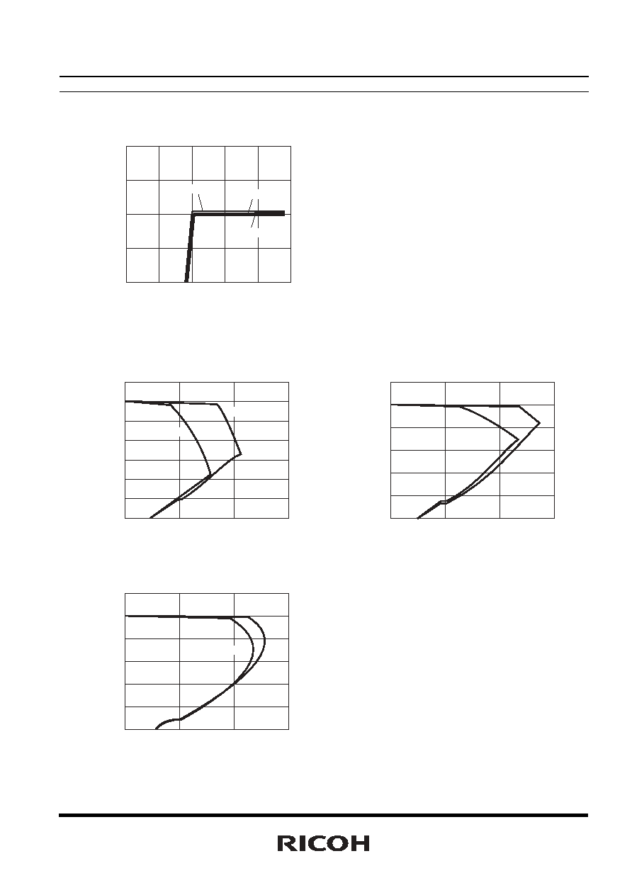
Output Delay Time for Release V
DET
In the R1150Hxx1C/D can set an output delay time for release voltage detector with connecting a capacitor to
C
D
pin. When an input voltage (in the case of R1150Hxx1C) or an output voltage (in the case of R1150Hxx1D)
surpasses the release voltage of its voltage detector (+V
DET
), the capacitor which is connected to C
D
pin is started
to be charged, as a result, C
D
pin voltage rises. When the C
D
pin voltage surpasses C
D
pin threshold voltage, the
output voltage of the voltage detector outputs "H".
Input Voltage or Output Voltage
C
D
Pin Voltage
Output Voltage
Output Delay Time (tpLH)
GND
GND
C
D
Pin Threshold Voltage
Released Voltage (+V
DET
)
Output delay time for release voltage detector can be calculated with the next formula:
tpLH=1.25/200◊10
9
◊
C (sec)
Input Transient Response
If input transient is 0.12V/µs or faster, the output response may be extremely worse than normal operation. In
that case, add a capacitor between V
IN
and GND, and make the transient speed of V
IN
slower than 0.12V/µs.
PACKAGE INFORMATION
PE-SOT-89-5-0512
∑
SOT-89-5
Unit: mm
PACKAGE DIMENSIONS
4.5
±0.1
1.5
±0.1
0.4
±0.1
1.6
±0.2
1.5
±0.1
1.5
±0.1
±0.1
2.5
±
0.1
0.42
±0.1
1.0
5
4
1
2
3
0.4
0.9
MIN.
+0.5
≠0.3
4.5
0.47
0.4
±0.1
0.42
±0.2
0.42
±0.2
TAPING SPECIFICATION (T1: Standard Type)
T 1
User Direction of Feed
T 2
2.5MAX.
0.3
±0.1
12
±
0.3
5.0
4.7
8.0
±0.1
4.0
±0.1
2.0
±0.05
5.65
±
0.05
1.5
±
0.1
1.5
+0.1
0
1.6±0.1
TAPING REEL DIMENSIONS
(1reel=1000pcs)
2
±0.5
60
180
≠1.5
+1 0
0
21
±0.8
15.4
±1.0
13
±0.3
13
±
0.2

PACKAGE INFORMATION
PE-SOT-89-5-0512
POWER DISSIPATION (SOT-89-5)
This specification is at mounted on board. Power Dissipation (P
D
) depends on conditions of mounting on board.
This specification is based on the measurement at the condition below:
Measurement Conditions
High Wattage Land Pattern
Standard Land Pattern
Environment
Mounting on Board (Wind velocity=0m/s)
Mounting on Board (Wind velocity=0m/s)
Board Material
Glass cloth epoxy plactic (Double sided)
Glass cloth epoxy plactic (Double sided)
Board
Dimensions
30mm
◊ 30mm ◊ 1.6mm
50mm
◊ 50mm ◊ 1.6mm
Copper Ratio
Top side : Approx. 20% ,
Back side : Approx. 100%
Top side : Approx. 10% ,
Back side : Approx. 100%
Through-hole
0.85mm ◊ 10pcs
-
Measurement Result
(Topt=25
∞C,Tjmax=125∞C)
High Wattage Land Pattern
Standard Land Pattern
Free Air
Power Dissipation
1300mW
900mW
500mW
Thermal Resistance
77
∞C/W 111∞C/W 200∞C/W
0
200
800
500
1100
1400
100
700
400
1000
1300
300
900
600
1200
1500
0
150
50
25
75 85 100
125
Power Dissipation P
D
(mW)
Ambient Temperature (
∞C)
On Board
(High Wattage Land Pattern)
On Board
(Standard Land Pattern)
Free Air
30
15
7.5
30
15
7.5
50
50
High Wattage
Standard
Power Dissipation
Measurement Board Pattern
IC Mount Area (Unit : mm)
RECOMMENDED LAND PATTERN (SOT-89-5)
1.0
0.7 MAX.
0.7 MAX.
1.5
1.5
45
∞
1.5
0.7
0.8
0.7
1.5
2.0
(Unit : mm)

MARK INFORMATIONS
ME-R1150H-0610
R1150H SERIES MARK SPECIFICATION
∑
SOT-89-5
1
2
3
4
5
6
1
: (fixed)
2
,
3
: Setting Voltage
(refer to Part Number vs. Product Code)
4
: Type (A,B,C,D)
5
,
6
: Lot Number
∑
Part Number vs. Product Code
Product Code
Product Code
Product Code
Product Code
Part Number
1
2
3
4
Part Number
1
2
3
4
Part Number
1
2
3
4
Part Number
1
2
3
4
R1150H001A D 0 1 A
R1150H002B D 0
2 B
R1150H007C D 0
7 C
R1150H002D D 0
2 D
R1150H002A D 0 2 A
R1150H003B D 0
3 B
R1150H008C D 0
8 C
R1150H016D D 1
6 D
R1150H003A D 0 3 A
R1150H004B D 0
4 B
R1150H009C D 0
9 C
R1150H017D D 1
7 D
R1150H006A D 0 6 A
R1150H005B D 0
5 B
R1150H020C D 2
0 C
R1150H018D D 1
8 D
R1150H010A D 1 0 A
R1150H006B D 0
6 B
R1150H041C D 4
1 C
R1150H020D D 2
0 D
R1150H011A D 1 1 A
R1150H021B D 2
1 B
R1150H022D D 2
2 D
R1150H012A D 1 2 A
R1150H024B D 2
4 B
R1150H026D D 2
6 D
R1150H013A D 1 3 A
R1150H025B D 2
5 B
R1150H028D D 2
8 D
R1150H014A D 1 4 A
R1150H035B D 3
5 B
R1150H030D D 3
0 D
R1150H015A D 1 5 A
R1150H036B D 3
6 B
R1150H031D D 3
1 D
R1150H019A D 1 9 A
R1150H037B D 3
7 B
R1150H021A D 2 1 A
R1150H038B D 3
8 B
R1150H023A D 2 3 A
R1150H027A D 2 7 A
R1150H029A D 2 9 A
R1150H033A D 3 3 A
R1150H039A D 3 9 A
R1150H040A D 4 0 A
R1150H042A D 4 2 A