 | –≠–ª–µ–∫—Ç—Ä–æ–Ω–Ω—ã–π –∫–æ–º–ø–æ–Ω–µ–Ω—Ç: R1151N | –°–∫–∞—á–∞—Ç—å:  PDF PDF  ZIP ZIP |

Boost type Voltage Regulator with Reset
R1151N SERIES
1
R1151N_E.doc/2003/07/14
NO. EA-092-0307
OUTLINE
The R1151N Series are CMOS-based boost type voltage regulator ICs with high output voltage accuracy, low sup-
ply current, and high ripple rejection. Each of these voltage regulator controllers consists of a voltage reference unit,
an error amplifier, comparators, resistors for output and reset voltage setting, a current limit protection circuit, and a
chip enable circuit.
In addition to low consumption current by CMOS process, the chip enable function prolongs the battery life. Dy-
namic response and ripple rejection of the R1151N Series are excellent, further these are low noise type, plus maxi-
mum operating input voltage tolerance is up to 18.5V, thus these ICs are very suitable for the power supply for hand-
held equipment and other power management applications using AC adapter input voltage.
The output voltage of these ICs is internally fixed with high accuracy. Since the package for these ICs is SOT-23-6
(Mini-mold) package, high density mounting of the ICs on boards is possible.
FEATURES
∑ Ultra-Low Supply Current ............................................... Typ. 70µA (I
OUT
=0mA)
∑ Standby Mode................................................................... Typ. 0.1µA
∑ Low Dropout Voltage ....................................................... Typ. 0.1V (I
OUT
=100mA *Depends on External Transistor)
∑ High Ripple Rejection ...................................................... Typ. 60dB (f=1kHz)
∑ Low Temperature-Drift Coefficient of Output Voltage .......Typ.±100ppm/∞C
∑ High Output Voltage Accuracy ........................................ ±2.0%
∑ Excellent Dynamic Response
∑ Small Package .................................................................. SOT-23-6 (Mini-mold)
∑ Output Voltage.................................................................. Stepwise setting with a step of 0.1V in the range of 2.5V to 9.0V
∑ Built-in chip enable circuit (2 types; A: active low, B: active high)
∑ Output Capacitor .............................................................. Tantalum type recommendation (or Ceramic+Series Resistor)
∑ Built-in output voltage detector ...................................... with delay (C version)
∑ Detector Threshold Tolerance......................................... ±2.5%
∑ Detector Threshold Voltage ............................................ Stepwise setting with a step of 0.1V in the range of 1.7V to 8.0V
∑ Operating Input Voltage ................................................... Max. 18.5V
APPLICATIONS
∑ Power source for handheld equipment such as cameras and videos.
∑ Power source for home appliances.
∑ Power source for battery-powered equipment.

R1151N
2
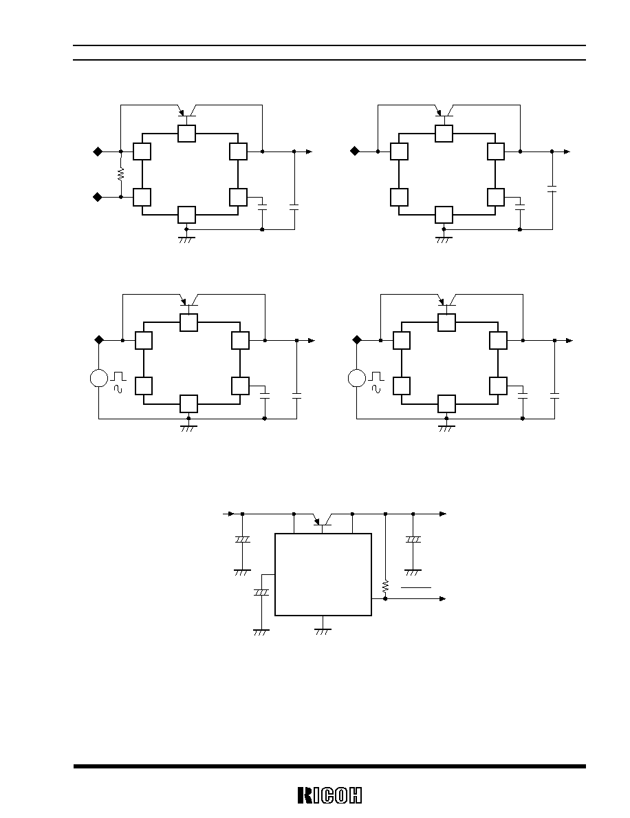
BLOCK DIAGRAMS
R1151NxxxB
6
2
5
V
OUT
GND
V
DD
V
DET
-
+
Vref
3
+
-
4
CE
Vref
EXT
1
Current Limit
R1151NxxxC
6
2
5
V
OUT
GND
V
DD
V
DET
-
+
Vref
3
+
-
4
CD
Vref
EXT
1
Current Limit
SELECTION GUIDE
The output voltage, mask option code, and the taping type for the ICs can be selected at the user's request. The
selection can be made with designating the part number as shown below;
R1151Nxxxx-xx
Part Number
a b c
Code
Contents
a
Code Number for Voltage Setting
b
Setting mask option :
A: with
CE (active at "L" type)
B: with CE (active at "H" type)
C: with the pin for external capacitor to set the output delay of voltage detector
c
Designation of Taping Type :
Ex. TR (Refer to Taping Specifications.)

R1151N
3
PIN CONFIGURATION
SOT-23-6
1
2
3
EXT
V
DET
V
OUT
6
4
(MARK SIDE)
5
V
DD
CE/CD
GND
PIN DESCRIPTIONS
Pin No.
Symbol
Description
1
EXT
External Transistor Drive Pin
2
V
DET
Voltage Detector Output Pin
3
V
OUT
Voltage Regulator Output pin
4
CE or CE
Chip Enable Pin (A/B version)
4
CD
Pin for External capacitor to set Output Delay of Voltage Detector (C version)
5
GND
Ground Pin
6
V
DD
Input Pin
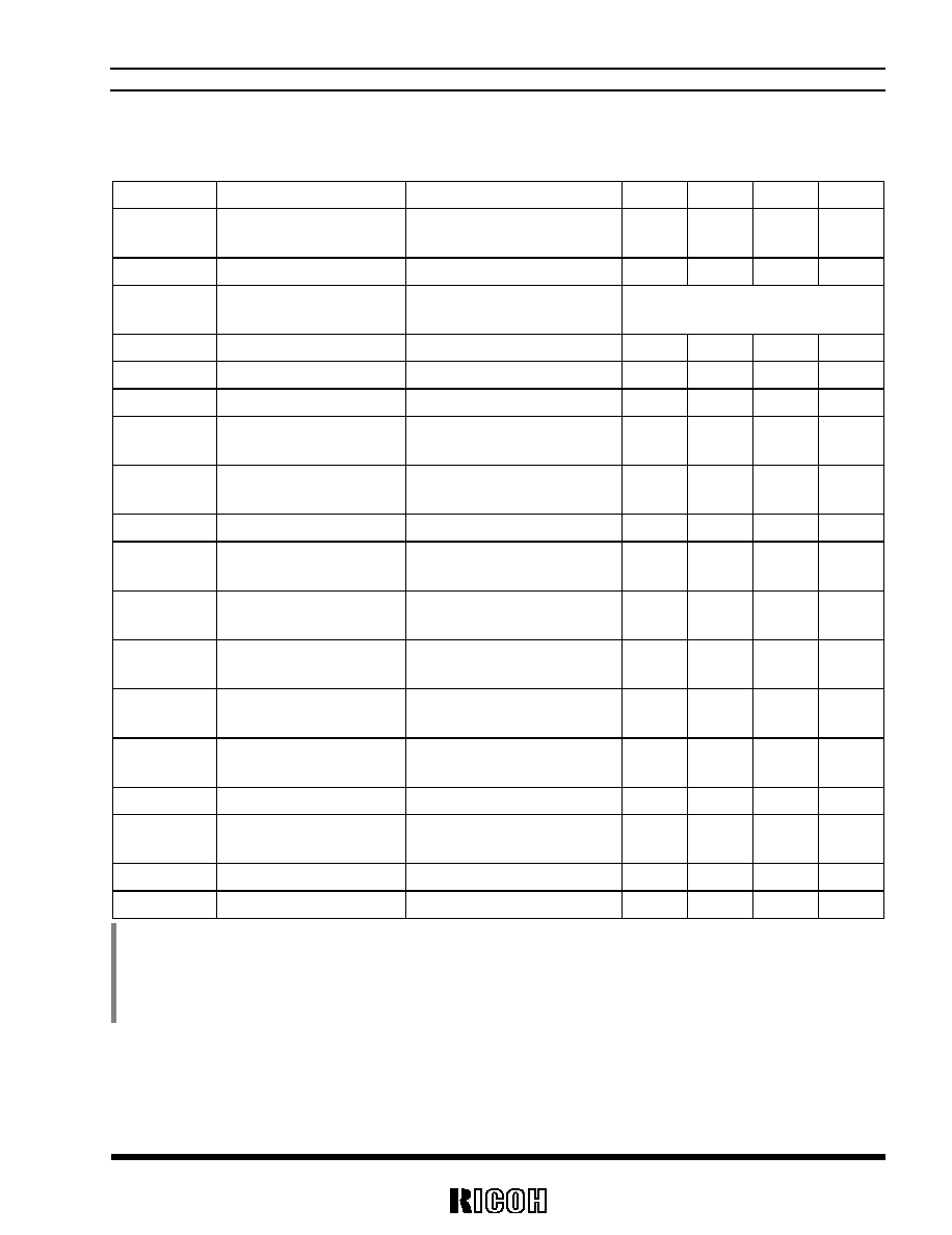
ABSOLUTE MAXIMUM RATINGS
Symbol
Item
Rating
Unit
V
IN
Input Voltage
20
V
V
CE/CD
Input Voltage (CE
/CE/CD Pin)
-0.3 V
IN
+0.3
V
V
OUT
Output Voltage (V
OUT
Pin)
-0.3 V
IN
+0.3
V
V
EXT
Output Voltage (EXT Pin)
-0.3 V
IN
+0.3
V
V
DET
Output Voltage (V
DET
Pin)
-0.3 V
IN
+0.3
V
I
EXT
EXT Output Current
30
mA
P
D
Power Dissipation
150
mW
Topt
Operating Temperature Range
-40 ~ 85
∞C
Tstg
Storage Temperature Range
-55 ~ 125
∞C

R1151N
4
ELECTRICAL CHARACTERISTICS
∑ R1151NxxxA/B
Topt=25∞C
Symbol
Item
Conditions
Min.
Typ.
Max.
Unit
V
OUT
Output Voltage
V
IN
= Set V
OUT
+1V
I
OUT
= 50mA
V
OUT
◊0.98
V
OUT
◊1.02
V
I
OUT
Output Current
V
IN
- V
OUT
= 1.0V
1
Note
A
V
OUT
/I
OUT
Load Regulation
V
IN
= Set V
OUT
+1V
1mA I
OUT
100mA
Refer to the Load Regulation Table
V
DIF
Dropout Voltage
I
OUT
= 100mA
0.1
Note
0.2
V
I
SS
Supply Current
V
IN
= Set V
OUT
+1V, I
OUT
= 0mA
70
100
µA
Istandby
Supply Current (Standby)
V
IN
= 18.5V
15
µA
I
EXT
leak
EXT Leakage Current
0.5
µA
V
OUT
/V
IN
Line Regulation
Set V
OUT
+0.5V V
IN
18.5V
I
OUT
= 50mA
0.00
0.02
0.10
%/V
RR
Ripple Rejection
f = 1kHz, Ripple 0.5Vp-p
V
IN
= Set V
OUT
+1V
60
dB
V
IN
Input Voltage
18.5
V
V
OUT
/T
Output Voltage
Temperature Coefficient
I
OUT
= 10mA
-40∞C Topt 85∞C
±100
ppm
/∞C
Ilim
Current Limit
Base Current I
B
of PNP Tr.
V
IN
- V
OUT
= 1.0V
8
27
mA
I
RPT
Short Current Limit
Base Current I
B
of PNP Tr.
V
OUT
= 0V
0.7
mA
R
UD
CE /CE Pull-up/down Resistance
2
M
V
CEH
CE /CE Input Voltage "H"
1.5
V
IN
V
V
CEL
CE /CE Input Voltage "L"
0.00
0.25
V
-V
DET
Detector Threshold
-V
DET
◊0.975
-V
DET
◊1.025
V
V
HYS
Detector Threshold
Hysteresis Range
-V
DET
◊0.03
-V
DET
◊0.05
-V
DET
◊0.07
V
I
OUT2
Output Current 2
V
DD
= 1.5V, V
DS
= 0.5V
2.0
5.0
10.0
mA
V
DET
/T
Detector Threshold
Temperature Coefficient
-40∞C Topt 85∞C
±100
ppm
/∞C
tPLH
Output Delay Time
0.1
ms
V
DDL
Minimum Operating Voltage
0.9
1.1
V
Note: This item depends on the capability of external PNP transistor. Use low saturation type transistor with
hFE value range of 100 to 300.
R1151N
5
∑ R1151NxxxC
Topt=25∞C
Symbol
Item
Conditions
Min.
Typ.
Max.
Unit
V
OUT
Output Voltage
V
IN
= Set V
OUT
+1V
I
OUT
= 50mA
V
OUT
◊
0.98
V
OUT
◊1.02
V
I
OUT
Output Current
V
IN
- V
OUT
= 1.0V
1
*Note1
A
V
OUT
/I
OUT
Load Regulation
V
IN
= Set V
OUT
+1V
1mA I
OUT
100mA
Refer to the Load Regulation Table
V
DIF
Dropout Voltage
I
OUT
= 100mA
0.1
*Note1
V
I
SS
Supply Current
V
IN
= Set V
OUT
+1V, I
OUT
= 0mA
70
100
µA
I
EXT
leak
EXT Leakage Current
0.5
µA
V
OUT
/V
IN
Line Regulation
Set V
OUT
+0.5V V
IN
18.5V
I
OUT
= 50mA
0.00
0.02
0.10
%/V
RR
Ripple Rejection
f = 1kHz, Ripple 0.5Vp-p
V
IN
= Set V
OUT
+1V
60
dB
V
IN
Input Voltage
18.5
V
V
OUT
/T
Output Voltage
Temperature Coefficient
I
OUT
= 10mA
-40∞C Topt 85∞C
±100
ppm
/∞C
Ilim
Current Limit
Base Current I
B
of PNP Tr.
V
IN
- V
OUT
= 1.0V
8
27
mA
I
RPT
Short Current Limit
Base Current I
B
of PNP Tr.
V
OUT
= 0V
0.7
mA
-V
DET
Detector Threshold
-V
DET
◊0.975
-V
DET
◊1.025
V
V
HYS
Detector Threshold
Hysteresis Range
-V
DET
◊0.03
-V
DET
◊0.05
-V
DET
◊0.07
V
I
OUT2
Output Current 2
V
DD
= 1.5V, V
DS
= 0.5V
2.0
5.0
10.0
mA
V
DET
/T
Detector Threshold
Temperature Coefficient
-40∞C Topt 85∞C
±100
ppm
/∞C
tPLH
Output Delay Time
CD=220pF
*Note2
0.9
1.6
2.7
ms
V
DDL
Minimum Operating Voltage
0.9
1.1
V
Note1:This item depends on the capability of external PNP transistor. Use low saturation type transistor with
hFE value range of 100 to 300.
Note2:V
DET
pin is pulled-up to V
DD
via 470k
resistance. The time is between the rising edge of V
OUT
level from
0.9V to (+V
DET
)+2.0V and the reaching point to ((+V
DET
)+2.0V)/2 of the V
DET
output voltage.
R1151N
6
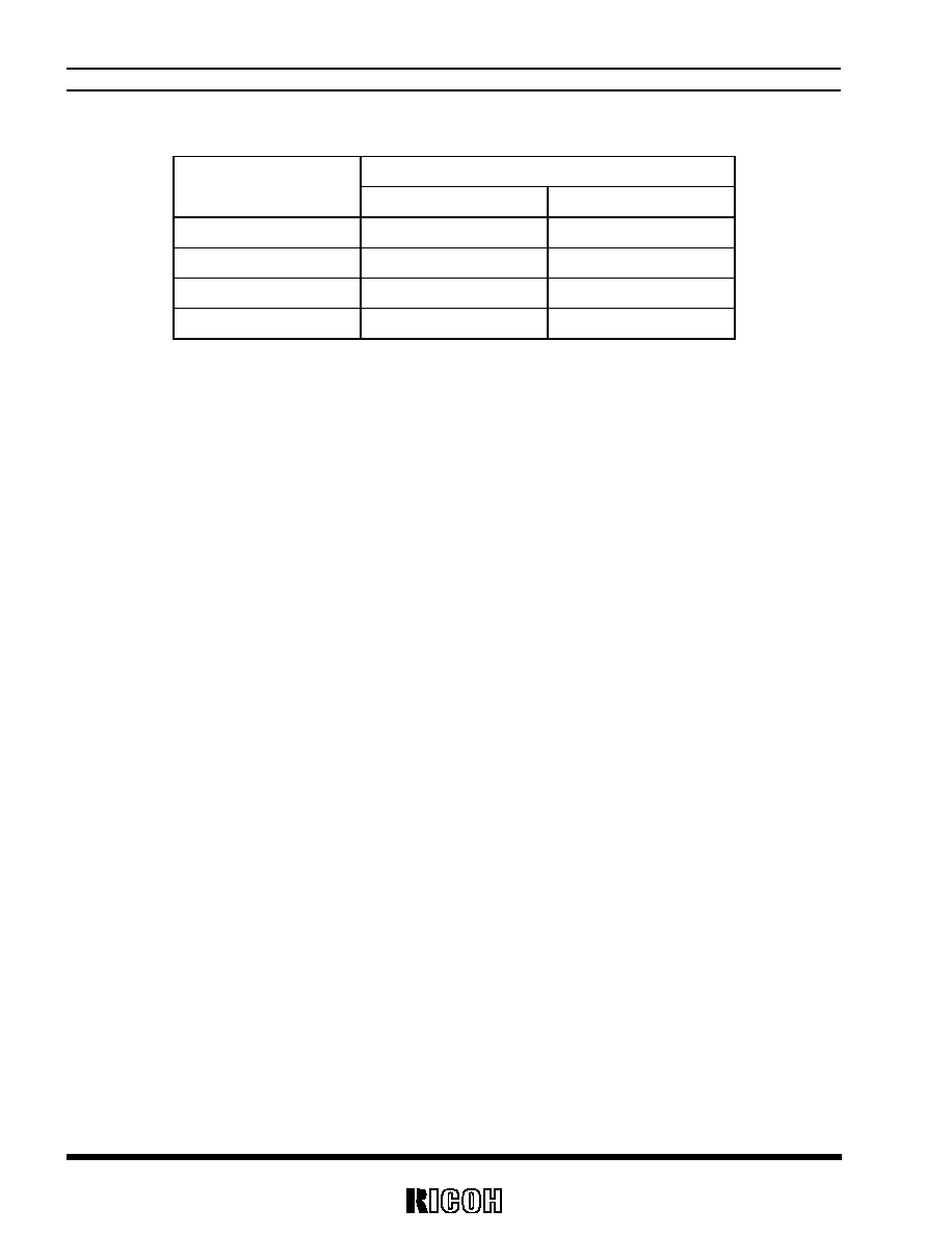
∑ Load Regulation Table
Load Regulation
V
OUT
/
I
OUT
(mV)
Output Voltage
V
OUT
(V)
Typ.
Max.
2.5 to 3.3
20
60
3.4 to 5.0
30
90
5.1 to 7.0
40
130
7.1 to 9.0
50
160
OPERATION
In these ICs, fluctuation of Output Voltage, V
OUT
is detected by the feed-back registers, and the result is compared
with a reference voltage with the error amplifier and control the base current of an external PNP transistor so that a
constant voltage is output. The base current is monitored with the base current limit circuit. If the base current may
be too large, the protection circuit works, further, output voltage is monitored with the built-in voltage detector. If the
set detector threshold voltage is detected, reset signal will be output.
TECHNICAL NOTES
When using these ICs, consider the following points:
In these ICs, phase compensation is made for securing stable operation even if the load current is varied. For this pur-
pose, be sure to use as much as 10µF capacitor as CL with good frequency characteristics and ESR (Equivalent Series
Resistance).
The best suitable equivalent series resistor value (ESR) is approximately 1.
If the ESR of the output capacitor is too large, output may be unstable, therefore fully evaluation is necessary.
Make V
DD
and GND lines sufficient. When their impedance of these is high, noise pickup or unstable operation may be
the result. Connect a capacitor with a capacitance value of as much as 10µF between V
DD
and GND as close as possible
to these pins.
Set external components, especially output capacitor, as close as possible to the ICs.
Refer to the next equation to calculate the output delay time of C version and decide the capacitance value for the de-
lay time.
tPLH =1.83◊C/(300◊10
-9
)
C: Capacitance value (F)
Recommended pull-up resistance (R1) value is 470k. If the value is too small, released voltage may shift, therefore,
use 10k or more value resistor.
R1151N
7
TEST CIRCUITS
6
3
4
2
R1151NxxC
R1
1
V
DET
V
IN
5
I
OUT
PNP
C2
C1
6
3
4
2
R1151NxxC
1
V
IN
5
I
OUT
PNP
C2
C1
Fig.1 Standard test Circuit
Fig.2 Supply Current Test Circuit
R1=470k
C1=220pF, C2=10µF
C1=220pF, C2=10µF
6
3
4
2
R1151NxxC
1
V
IN
5
I
OUT
PNP
C2
C1
P.G.
6
3
4
2
R1151NxxC
1
V
IN
5
I
OUT
PNP
C2
C1
P.G.
Fig.3 Ripple Rejection, Line Transient Response Test Circuit Fig.4 Load Transient Response Test Circuit
C1=220pF, C2=10µF
C1=220pF, C2=10µF
TYPICAL APPLICATION
CD
V
DET
R1151NxxxC
GND
OUT
EXT
V
OUT
CL
R1
V
DD
RESET
+
CI
+
CD
+
IN
PNP Tr
(External Components)
C1 10µF R1=470k PNP Tr.: 2SA1441, 2SB940, 2SB703
CL 10µF
R1151N
8
TYPICAL CHARACTERISTICS
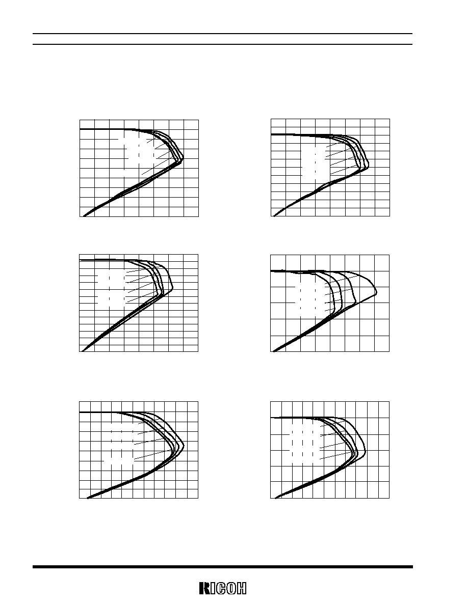
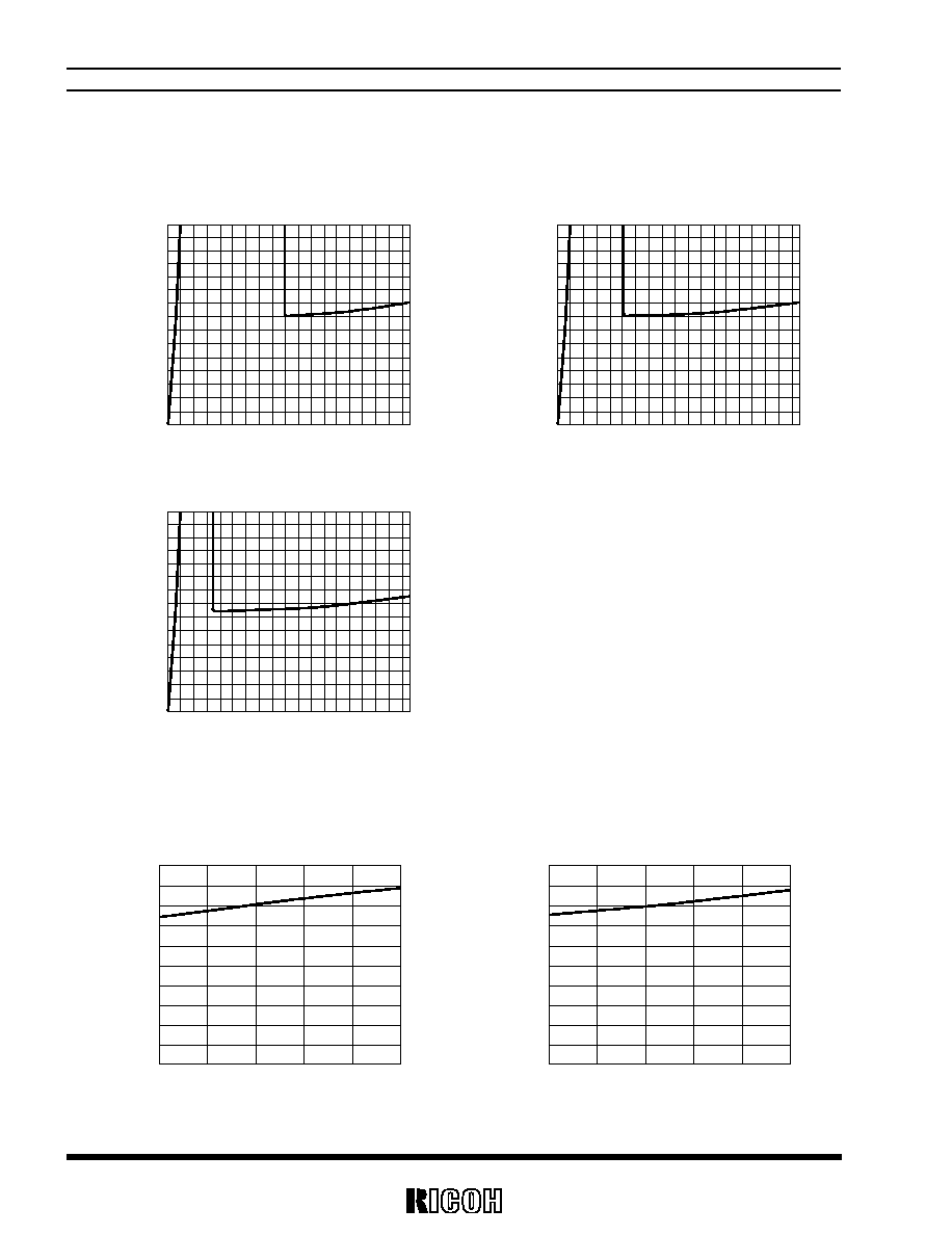
1)
Output Voltage vs. Output Current (Topt=25∞C)
a.
External Tr.: 2SA1441
R1151N (VR=9.0V)
R1151N (VR=5.0V)
10.00
9.00
8.00
7.00
5.00
4.00
6.00
3.00
2.00
1.00
0.00
Output Current I
OUT
(mA)
Output Voltage V
ROUT
(V)
0
500 1000
2000 2500
3500 4000
3000
1500
V
IN
=9.3V
V
IN
=9.5V
V
IN
=11V
V
IN
=10V
6.00
5.50
5.00
4.50
4.00
3.50
3.00
2.50
2.00
1.50
1.00
0.50
0.00
Output Current I
OUT
(mA)
Output Voltage V
ROUT
(V)
0
500 1000
2000 2500
3500 4000
3000
1500
V
IN
=5.3V
V
IN
=5.5V
V
IN
=6V
V
IN
=7V
R1151N (VR=3.3V)
R1151N (VR=2.5V)
3.50
3.25
0.00
Output Current I
OUT
(mA)
Output Voltage V
ROUT
(V)
0
500 1000
2000 2500
3500 4000
3000
1500
3.00
2.75
2.50
2.25
2.00
1.75
1.50
1.25
1.00
0.75
0.50
0.25
V
IN
=5.3V
V
IN
=4.3V
V
IN
=3.8V
V
IN
=3.6V
0.00
Output Current I
OUT
(mA)
Output Voltage V
ROUT
(V)
0
500 1000
2000 2500
3500 4000
3000
1500
1.50
2.50
2.00
1.00
0.50
3.00
V
DD
=4.5V
V
DD
=3.5V
V
DD
=3.0V
V
DD
=2.8V
b.
External Tr.:2SB940
R1151N (VR=9.0V)
R1151N (VR=5.0V)
0.00
Output Current I
OUT
(mA)
Output Voltage V
ROUT
(V)
0 100 200 300 400 500 600 700 800
1000 1100
900
9.00
8.00
7.00
6.00
5.00
4.00
3.00
2.00
1.00
10.00
V
DD
=11.0V
V
DD
=10.0V
V
DD
=9.5V
V
DD
=9.3V
0.00
Output Current I
OUT
(mA)
Output Voltage V
ROUT
(V)
0 100 200 300 400 500 600 700 800
1000 1100
900
5.00
4.00
3.00
2.00
1.00
6.00
V
DD
=7.0V
V
DD
=6.0V
V
DD
=5.3V
V
DD
=5.5V

R1151N
9
R1151N (VR=3.3V)
R1151N (VR=2.5V)
0.00
Output Current I
OUT
(mA)
Output Voltage V
ROUT
(V)
0 100 200 300 400 500 600 700 800
1000 1100
900
3.50
3.00
2.50
2.00
1.50
1.00
0.50
4.00
V
DD
=5.3V
V
DD
=4.3V
V
DD
=3.8V
V
DD
=3.6V
0.00
Output Current I
OUT
(mA)
Output Voltage V
ROUT
(V)
0 100 200 300 400 500 600 700 800
1000 1100
900
2.50
2.00
1.50
1.00
0.50
3.00
V
DD
=4.5V
V
DD
=3.5V
V
DD
=3.0V
V
DD
=2.8V
c.
External Tr.:2SB703
R1151N (VR=9.0V)
R1151N (VR=5.0V)
0.00
Output Current I
OUT
(mA)
Output Voltage V
ROUT
(V)
0 100 200 300 400 500 600 700 800
1000 1100
900
9.00
8.00
7.00
6.00
5.00
4.00
3.00
2.00
1.00
10.00
V
IN
=11.0V
V
IN
=10.0V
V
IN
=9.5V
V
IN
=9.3V
0.00
Output Current I
OUT
(mA)
Output Voltage V
ROUT
(V)
0 100 200 300 400 500 600 700 800
1000 1100
900
5.00
4.00
3.00
2.00
1.00
6.00
V
IN
=7.0V
V
IN
=6.0V
V
IN
=5.5V
V
IN
=5.3V
R1151N (VR=3.3V)
R1151N (VR=2.5V)
0.00
Output Current I
OUT
(mA)
Output Voltage V
ROUT
(V)
0 100 200 300 400 500 600 700 800
1000 1100
900
0.50
1.00
1.50
2.00
2.50
3.00
3.50
V
IN
=5.3V
V
IN
=4.3V
V
IN
=3.8V
V
IN
=3.6V
0.00
Output Current I
OUT
(mA)
Output Voltage V
ROUT
(V)
0 100 200 300 400 500 600 700 800
1000 1100
900
2.50
3.00
2.00
1.50
1.00
0.50
V
IN
=4.5V
V
IN
=3.5V
V
IN
=3.0V
V
IN
=2.8V

R1151N
10
d.
Output Voltage vs. Base Current (Topt=25∞C)
VR=9.0V
VR=5.0V
0.00
Base Current I
EXT
(mA)
Output Voltage V
ROUT
(V)
0
2
16
18
14
12
10
8
6
4
9.00
10.00
8.00
7.00
6.00
4.00
5.00
3.00
2.00
1.00
0.00
Base Current I
EXT
(mA)
Output Voltage V
ROUT
(V)
0
2
16
18
14
12
10
8
6
4
5.00
6.00
4.00
3.00
2.00
1.00
VR=3.3V
VR=2.5V
0.00
Base Current I
EXT
(mA)
Output Voltage V
ROUT
(V)
0
2
16
14
12
10
8
6
4
4.00
3.50
3.00
2.50
2.00
1.50
1.00
0.50
0.00
Base Current I
EXT
(mA)
Output Voltage V
ROUT
(V)
0
2
18
16
14
12
10
8
6
4
3.00
2.75
2.50
2.25
2.00
1.75
1.50
1.25
1.00
0.75
0.50
0.25
2)
Output Voltage vs. Input Voltage (Topt=25∞C)
External Transistor: 2SA1441
R1151N (VR=5.0V)
R1151N (VR=3.3V)
1.00
Input Voltage V
IN
(V)
Output Voltage V
OUT
(V)
0 1 2 3
17 18
14 15 16
13
12
10 11
8 9
6 7
5
4
6.00
5.00
4.00
3.00
2.00
I
OUT
=0mA
I
OUT
=500mA
1.00
Input Voltage V
IN
(V)
Output Voltage V
OUT
(V)
0 1 2 3
17 18
14 15 16
13
12
10 11
8 9
6 7
5
4
4.00
3.50
3.00
2.50
2.00
1.50
I
OUT
=0mA
I
OUT
=500mA

R1151N
11
R1151N (VR=2.5V)
1.00
Input Voltage V
IN
(V)
Output Voltage V
OUT
(V)
0 1 2 3
17 18
14 15 16
13
12
10 11
8 9
6 7
5
4
3.00
2.75
2.50
2.25
2.00
1.50
1.75
1.25
I
OUT
=0mA
I
OUT
=500mA
3)
Output Voltage vs. Temperature
R1151N (VR=5.0V)
R1151N (VR=3.3V)
5.125
5.075
4.875
Temperature Topt(
∞C)
Output Voltage V
ROUT
(V)
-40
-15
85
5.025
4.975
4.925
10
35
60
V
IN
=6.0V
I
OUT
=80mA
3.375
3.355
3.215
Temperature Topt(
∞C)
Output Voltage V
ROUT
(V)
-40
-15
85
3.335
3.315
3.295
3.275
3.255
3.235
10
35
60
V
IN
=4.3V
I
OUT
=80mA
R1151N (VR=2.5V)
2.538
2.438
Temperature Topt(
∞C)
Output Voltage V
ROUT
(V)
-40
-15
85
2.513
2.488
2.463
10
35
60
V
IN
=3.5V
I
OUT
=80mA
R1151N
12
4)
Supply Current vs. Input Voltage
External Tr.:2SA1441
R1151N (VR=9.0V, -VD=8.0V)
R1151N (VR=5.0V, -VD=4.2V)
150
140
0
Input Voltage V
IN
(V)
0
10
20
40
30
60
50
80
70
100
90
120
110
130
18
17
1 2 3 4 5 6 7 8 9 10 1112 13 1415 16
I
OUT
=0mA
Supply Current I
SS
(
µ
A)
150
140
0
Input Voltage V
IN
(V)
0
10
20
40
30
60
50
80
70
100
90
120
110
130
18
17
1 2 3 4 5 6 7 8 9 10 1112 13 1415 16
I
OUT
=0mA
Supply Current I
SS
(
µ
A)
R1151N (VR=3.3V, -VD=2.9V)
150
140
0
Input Voltage V
IN
(V)
0
10
20
40
30
60
50
80
70
100
90
120
110
130
18
17
1 2 3 4 5 6 7 8 9 10 1112 13 1415 16
I
OUT
=0mA
Supply Current I
SS
(
µ
A)
5)
Supply Current vs. Temperature
a.
External Tr.:2SA1441
R1151N (VR=9.0V)
R1151N (VR=5.0V)
100
90
0
Temperature Topt(
∞C)
-40
-15
85
80
70
60
50
40
30
20
10
10
35
60
V
IN
=10V
I
OUT
=0mA
Supply Current I
SS
(
µ
A)
100
90
0
Temperature Topt(
∞C)
-40
-15
85
80
70
60
50
40
30
20
10
10
35
60
V
IN
=6V
I
OUT
=0mA
Supply Current I
SS
(
µ
A)

R1151N
13
R1151N (VR=3.3V)
R1151N (VR=2.5V)
100
90
0
Temperature Topt(
∞C)
-40
-15
85
80
70
60
50
40
30
20
10
10
35
60
Supply Current I
SS
(
µ
A)
100
90
0
Temperature Topt(
∞C)
-40
-15
85
80
70
60
50
40
30
20
10
10
35
60
Supply Current I
SS
(
µ
A)
b.
External Tr.:2SB703
R1151N (VR=9.0V)
R1151N (VR=5.0V)
100
90
0
Temperature Topt(
∞C)
-40
-15
85
80
70
60
50
40
30
20
10
10
35
60
Supply Current I
SS
(
µ
A)
100
90
0
Temperature Topt(
∞C)
-40
-15
85
80
70
60
50
40
30
20
10
10
35
60
Supply Current I
SS
(
µ
A)
R1151N (VR=3.3V)
R1151N (VR=2.5V)
100
90
0
Temperature Topt(
∞C)
-40
-15
85
80
70
60
50
40
30
20
10
10
35
60
Supply Current I
SS
(
µ
A)
100
90
0
Temperature Topt(
∞C)
-40
-15
85
80
70
60
50
40
30
20
10
10
35
60
Supply Current I
SS
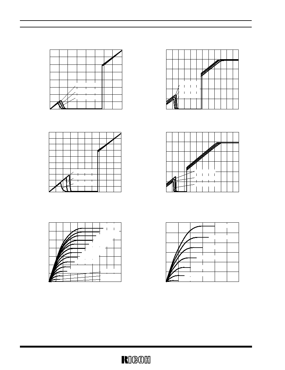
(
µ
A)

R1151N
14
6)
Ripple Rejection vs. Ripple Frequency (Topt=25∞C)
R1151N (VR=9.0V)
R1151N (VR=5.0V)
80
60
10
0
Ripple Frequency (kHz)
Ripple Rejection RR(dB)
0.01
0.1
1
10
100
50
40
30
20
70
V
IN
=10Vdc+0.5Vp-p, Iout=50mA, CL=10
µF
2SB703
2SA1441
2SB940
80
60
10
0
Ripple Frequency (kHz)
Ripple Rejection RR(dB)
0.01
0.1
1
10
100
50
40
30
20
70
V
IN
=6Vdc+0.5Vp-p, Iout=50mA, CL=10
µF
2SB703
2SA1441
2SB940
R1151N (VR=3.3V)
R1151N (VR=2.5V)
80
60
10
0
Ripple Frequency (kHz)
Ripple Rejection RR(dB)
0.01
0.1
1
10
100
50
40
30
20
70
V
IN
=4.3Vdc+0.5Vp-p, Iout=50mA, CL=10
µF
2SB703
2SA1441
2SB940
70
10
0
Ripple Frequency (kHz)
Ripple Rejection RR(dB)
0.01
0.1
1
10
100
20
30
40
50
60
V
IN
=3.5Vdc+0.5Vp-p, Iout=50mA, CL=10
µF
2SB703
2SA1441
2SB940
7)
Ripple Rejection vs. Temperature
R1151N (VR=5.0V)
R1151N (VR=3.3V)
Ripple Rejection RR(dB)
V
IN
=6Vdc+0.5Vp-p, Iout=50mA, CL=10
µF
75
73
Temperature Topt(
∞C)
-40
-15
85
71
69
67
65
63
61
59
57
55
10
35
60
2SB703
2SA1441
2SB940
Ripple Rejection RR(dB)
V
IN
=4.3Vdc+0.5Vp-p, Iout=50mA, CL=10
µF
75
73
Temperature Topt(
∞C)
-40
-15
85
71
69
67
65
63
61
59
57
55
10
35
60
2SB703
2SA1441
2SB940
R1151N
15
R1151N (VR=2.5V)
Ripple Rejection RR(dB)
V
IN
=3.5Vdc+0.5Vp-p, Iout=50mA, CL=10
µF
70
Temperature Topt(
∞C)
-40
-15
85
65
60
55
50
45
10
35
60
2SB703
2SA1441
2SB940
8)
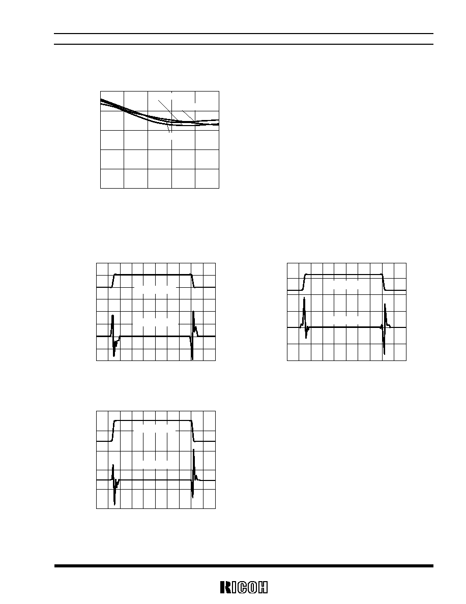
Input Transient Response(Topt=25∞C)
a.
External Tr.:2SA1441
R1151N (VR=5.0V)
R1151N (VR=3.3V)
I
OUT
=50mA
C
OUT
=Ceramic 10
µF
5.030
4.990
7
6
5
4
3
2
1
0
8
Time (
µs)
Input Voltage V
IN
(V)
25
0
Output Voltage V
OUT
(V)
50 75 100 125 150 175 200 225 250
5.020
5.010
5.000
Input Voltage
Output Voltage
I
OUT
=50mA
C
OUT
=Ceramic 10
µF
3.340
3.280
5
0
6
Time (
µs)
Input Voltage V
IN
(V)
25
0
Output Voltage V
OUT
(V)
50 75 100 125 150 175 200 225 250
3.330
4
3.320
3
3.310
2
3.300
1
3.290
Input Voltage
Output Voltage
R1151N (VR=2.5V)
I
OUT
=50mA
C
OUT
=Ceramic 10
µF
2.535
2.485
4
0
5
Time (
µs)
Input Voltage V
IN
(V)
25
0
Output Voltage V
OUT
(V)
50 75 100 125 150 175 200 225 250
2.525
3
2.515
2
2.505
1
2.495
Input Voltage
Output Voltage

R1151N
16
b.
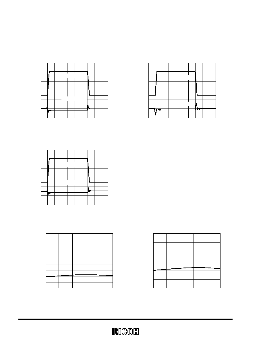
External Tr.: 2SB703
R1151N (VR=5.0V)
R1151N (VR=3.3V)
I
OUT
=50mA
C
OUT
=Ceramic 10
µF
5.030
4.990
7
0
8
Time (
µs)
Input Voltage V
IN
(V)
25
0
Output Voltage V
OUT
(V)
50 75 100 125 150 175 200 225 250
5.025
6
5.020
5
5.015
4
5.010
3
5.005
2
5.000
1
4.995
Input Voltage
Output Voltage
I
OUT
=50mA
C
OUT
=Ceramic 10
µF
3.340
3.280
5
0
6
Time (
µs)
Input Voltage V
IN
(V)
25
0
Output Voltage V
OUT
(V)
50 75 100 125 150 175 200 225 250
3.330
4
3.320
3
3.310
2
3.300
1
3.290
Input Voltage
Output Voltage
R1151N (VR=2.5V)
I
OUT
=50mA
C
OUT
=Ceramic 10
µF
2.535
2.485
4
0
5
Time (
µs)
Input Voltage V
IN
(V)
25
0
Output Voltage V
OUT
(V)
50 75 100 125 150 175 200 225 250
2.525
3
2.515
2
2.505
1
2.495
Input Voltage
Output Voltage
c.
External Tr. : 2SB940
R1151N (VR=5.0V)
R1151N (VR=3.3V)
I
OUT
=50mA
C
OUT
=Ceramic 10
µF
5.030
4.990
0
8
Time (
µs)
Input Voltage V
IN
(V)
25
0
Output Voltage V
OUT
(V)
50 75 100 125 150 175 200 225 250
6
5.020
7
5.025
5
5.015
4
5.010
3
5.005
1
4.995
2
5.000
Input Voltage
Output Voltage
I
OUT
=50mA
C
OUT
=Ceramic 10
µF
3.340
3.280
0
6
Time (
µs)
Input Voltage V
IN
(V)
25
0
Output Voltage V
OUT
(V)
50 75 100 125 150 175 200 225 250
5
3.330
4
3.320
3
3.310
2
3.300
1
3.290
Input Voltage
Output Voltage

R1151N
17
R1151N (VR=2.5V)
I
OUT
=50mA
C
OUT
=Ceramic 10
µF
2.535
2.485
0
5
Time (
µs)
Input Voltage V
IN
(V)
25
0
Output Voltage V
OUT
(V)
50 75 100 125 150 175 200 225 250
4
2.525
3
2.515
2
2.505
1
2.495
Input Voltage
Output Voltage
9)
Load Transient Response (Topt=25∞C)
a:
External Tr.: 2SA1441
R1151N (VR=5.0V)
R1151N (VR=3.3V)
V
IN
=6.0V
C
IN
=Ceramic 4.7
µF
C
OUT
=Ceramic 10
µF
5.05
4.99
0
120
Time (
µs)
Output Current I
OUT
(mA)
100
0
Output Voltage V
OUT
(V)
200 300 400 500 600 700 800 900 1000
100
5.04
80
5.03
60
5.02
40
5.01
20
5.00
Output Voltage
Output Current
V
IN
=4.3V
C
IN
=Ceramic 4.7
µF
C
OUT
=Ceramic 10
µF
3.35
3.29
0
120
Time (
µs)
Output Current I
OUT
(mA)
100
0
Output Voltage V
OUT
(V)
200 300 400 500 600 700 800 900 1000
100
3.34
80
3.33
60
3.32
40
3.31
20
3.30
Output Voltage
Output Current
R1151N (VR=2.5V)
V
IN
=3.5V
C
IN
=Ceramic 4.7
µF
C
OUT
=Ceramic 10
µF
2.55
2.49
0
120
Time (
µs)
Output Current I
OUT
(mA)
100
0
Output Voltage V
OUT
(V)
200 300 400 500 600 700 800 900 1000
100
2.54
80
2.53
60
2.52
40
2.51
20
2.50
Output Current
Output Voltage
R1151N
18
b.
External Tr.: 2SB703
R1151N (VR=5.0V)
R1151N (VR=3.3V)
V
IN
=6.0V
C
IN
=Ceramic 4.7
µF
C
OUT
=Ceramic 10
µF
5.05
4.99
0
120
Time (
µs)
Output Current I
OUT
(mA)
100
0
Output Voltage V
OUT
(V)
200 300 400 500 600 700 800 900 1000
100
5.04
80
5.03
60
5.02
40
5.01
20
5.00
Output Voltage
Output Current
V
IN
=4.3V
C
IN
=Ceramic 4.7
µF
C
OUT
=Ceramic 10
µF
3.35
3.29
0
120
Time (
µs)
Output Current I
OUT
(mA)
100
0
Output Voltage V
OUT
(V)
200 300 400 500 600 700 800 900 1000
100
3.34
80
3.33
60
3.32
40
3.31
20
3.30
Output Current
Output Voltage
R1151N (VR=2.5V)
V
IN
=3.5V
C
IN
=Ceramic 4.7
µF
C
OUT
=Ceramic 10
µF
2.55
2.49
0
120
Time (
µs)
Output Current I
OUT
(mA)
100
0
Output Voltage V
OUT
(V)
200 300 400 500 600 700 800 900 1000
100
2.54
80
2.53
60
2.52
40
2.51
20
2.50
Output Current
Output Voltage
10) Detector Threshold vs. Temperature
R1151N (-V
DET
=8.0V)
R1151N (-V
DET
=4.2V)
8.70
8.60
7.80
Temperature Topt(
∞C)
Detector Threshold V
DET
(V)
-40
-15
85
8.50
8.40
8.30
8.20
8.10
8.00
7.90
10
35
60
4.60
4.00
Temperature Topt(
∞C)
Detector Threshold V
DET
(V)
-40
-15
85
4.50
4.40
4.30
4.20
4.10
10
35
60
R1151N
19
R1151N (-V
DET
=2.9V)
R1151N (-V
DET
=1.7V)
3.10
2.80
Temperature Topt(
∞C)
Detector Threshold V
DET
(V)
-40
-15
85
3.05
3.00
2.95
2.90
2.85
10
35
60
1.85
1.60
Temperature Topt(
∞C)
Detector Threshold V
DET
(V)
-40
-15
85
1.80
1.75
1.70
1.65
10
35
60
11) V
DET
Output Voltage vs. Input Voltage
R1151N (-V
DET
=8.0V Pull-up to V
DD
)
R1151N (-V
DET
=8.0V Pull-up to 5V)
9.0
8.0
6.0
5.0
3.0
2.0
0.0
1.0
Input Voltage V
IN
(V)
V
DET
Output Voltage VD
OUT
(V)
0
1
3
5
6
8
9
4.0
4
7
2
7.0
Topt=-40
∞C
Topt=25
∞C
Topt=85
∞C
6.00
5.00
4.00
2.00
0.00
1.00
Input Voltage V
IN
(V)
V
DET
Output Voltage VD
OUT
(V)
0
1
3
5
6
8
9
3.00
4
7
2
Topt=-40
∞C
Topt=25
∞C
Topt=85
∞C
R1151N (-V
DET
=4.2V Pull-up to V
DD
)
R1151N (-V
DET
=4.2V Pull-up to 5V)
5.0
4.5
3.5
3.0
1.5
1.0
0.0
0.5
Input Voltage V
IN
(V)
V
DET
Output Voltage VD
OUT
(V)
0 0.5
2
3 3.5
4.5 5
2.0
2.5
2.5
4
1 1.5
4.0
Topt=-40
∞C
Topt=25
∞C
Topt=85
∞C
6.0
5.0
4.0
2.0
0.0
1.0
Input Voltage V
IN
(V)
V
DET
Output Voltage VD
OUT
(V)
0 0.5
2
3.5 4
5.5 6
3.0
2.5 3
5
4.5
1 1.5
Topt=-40
∞C
Topt=25
∞C
Topt=85
∞C
R1151N
20
R1151N (-V
DET
=2.9V Pull-up to V
DD
)
R1151N (-V
DET
=2.9V Pull-up to 5V)
4.0
3.5
3.0
2.5
1.0
0.0
0.5
Input Voltage V
IN
(V)
V
DET
Output Voltage VD
OUT
(V)
0
0.5
2
3
3.5
1.5
2.0
2.5
4
1
1.5
Topt=-40
∞C
Topt=25
∞C
Topt=85
∞C
6.0
5.0
4.0
2.0
0.0
1.0
Input Voltage V
IN
(V)
V
DET
Output Voltage VD
OUT
(V)
0 0.5
2
3.5 4
5.5 6
3.0
2.5 3
5
4.5
1 1.5
Topt=-40
∞C
Topt=25
∞C
Topt=85
∞C
R1151N (-V
DET
=1.7V Pull-up to V
DD
)
R1151N (-V
DET
=1.7V Pull-up to 5V)
2.5
2.3
1.8
1.5
0.8
0.5
0.0
0.3
Input Voltage V
IN
(V)
V
DET
Output Voltage VD
OUT
(V)
0 0.25
1
1.5 1.75
2.25 2.5
1.0
1.3
1.25
2
0.5 0.75
2.0
Topt=-40
∞C
Topt=25
∞C
Topt=85
∞C
6.0
5.0
4.0
2.0
0.0
1.0
Input Voltage V
IN
(V)
V
DET
Output Voltage VD
OUT
(V)
0 0.5
2
3.5 4
5.5 6
3.0
2.5 3
5
4.5
1 1.5
Topt=-40
∞C
Topt=25
∞C
Topt=85
∞C
12) Nch Driver Output Current vs. V
DS
(Topt=25∞C)
R1151N (-V
DET
=8.0V)
R1151N (-V
DET
=4.2V)
140
120
60
100
80
40
20
0
V
DS
(V)
Output Current I
OUT
(mA)
0
1
2
3
4
6
10
5
7
8
9
V
DD
=7.5V
V
DD
=7.0V
V
DD
=6.5V
V
DD
=6.0V
V
DD
=5.5V
V
DD
=5.0V
V
DD
=4.5V
V
DD
=4.0V
V
DD
=3.5V
V
DD
=3.0V
V
DD
=2.5V
V
DD
=2.0V
V
DD
=1.5V
V
DD
=1.0V
60
50
20
40
30
10
0
V
DS
(V)
Output Current I
OUT
(mA)
0
1
2
3
4
6
5
V
DD
=4.0V
V
DD
=3.5V
V
DD
=3.0V
V
DD
=2.5V
V
DD
=2.0V
V
DD
=1.5V
V
DD
=1.0V
R1151N
21
R1151N (-V
DET
=2.9V)
R1151N (-V
DET
=1.7V)
30
25
10
20
15
5
0
V
DS
(V)
Output Current I
OUT
(mA)
0
0.5
1
1.5
2
3
2.5
V
DD
=2.5V
V
DD
=2.0V
V
DD
=1.5V
V
DD
=1.0V
8
7
3
5
4
1
0
V
DS
(V)
Output Current I
OUT
(mA)
0
0.5
1
1.5
2
2
6
V
DD
=1.5V
V
DD
=1.25V
V
DD
=1.0V
13) Nch Driver Output Current vs. Input Voltage
R1151N (-V
DET
=8.0V)
R1151N (-V
DET
=4.2V)
Output Current I
OUT
(mA)
40
35
25
20
15
10
0
Input Voltage V
IN
(V)
0
2
6
8
10
5
30
4
Topt=25
∞C
Topt=-40
∞C
Topt=85
∞C
Output Current I
OUT
(mA)
40
35
25
20
15
10
0
Input Voltage V
IN
(V)
0
1
3
4
5
5
30
2
Topt=25
∞C
Topt=-40
∞C
Topt=85
∞C
R1151N (-V
DET
=2.9V)
R1151N (-V
DET
=1.7V)
Output Current I
OUT
(mA)
40
35
25
20
15
10
0
Input Voltage V
IN
(V)
0
1
3
4
5
30
2
Topt=25
∞C
Topt=-40
∞C
Topt=85
∞C
Output Current I
OUT
(mA)
40
35
25
20
15
10
0
Input Voltage V
IN
(V)
0
1
2
2.5
5
30
0.5
1.5
Topt=25
∞C
Topt=-40
∞C
Topt=85
∞C

R1151N
22
14) CD pin Threshold Voltage vs. Temperature
R1151N (-V
DET
=8.0V)
R1151N (-V
DET
=1.7V)
3.0
1.8
1.4
2.2
2.8
1.0
Temperature Topt(
∞C)
CD pin Threshold Voltage Vtcd(V)
-40
10
35
85
1.6
1.2
2.0
2.6
2.4
-15
60
H
L
L
H
3.0
1.8
1.4
2.2
2.8
1.0
Temperature Topt(
∞C)
CD pin Threshold Voltage Vtcd(V)
-40
10
35
85
1.6
1.2
2.0
2.6
2.4
-15
60
H
L
L
H
15) CD Pin Output Current vs. Input Voltage
R1151N (-V
DET
=8.0V)
R1151N (-V
DET
=4.2V)
0.45
0.40
0.25
0.15
0.05
0.00
Input Voltage V
IN
(V)
CD pin Output Current I
OUT
(mA)
0.0
4.0
2.0
6.0
8.0 9.0
0.10
0.20
0.35
0.30
3.0
1.0
7.0
5.0
Topt=-40
∞C
Topt=25
∞C
Topt=85
∞C
0.45
0.40
0.25
0.15
0.05
0.00
Input Voltage V
IN
(V)
CD pin Output Current I
OUT
(mA)
0.0
2.5
1.0
3.5
4.5 5.0
0.10
0.20
0.35
0.30
1.5
0.5
4.0
2.0
3.0
Topt=-40
∞C
Topt=25
∞C
Topt=85
∞C
R1151N (-V
DET
=2.9V)
R1151N (-V
DET
=1.7V)
0.45
0.40
0.25
0.15
0.05
0.00
Input Voltage V
IN
(V)
CD pin Output Current I
OUT
(mA)
0.0
2.5
1.0
3.5
0.10
0.20
0.35
0.30
1.5
0.5
2.0
3.0
Topt=-40
∞C
Topt=25
∞C
Topt=85
∞C
0.45
0.40
0.25
0.15
0.05
0.00
Input Voltage V
IN
(V)
CD pin Output Current I
OUT
(mA)
0.0
1.4
0.6
2.0
0.10
0.20
0.35
0.30
0.8 1.0
0.2 0.4
1.6
1.2
1.8
Topt=-40
∞C
Topt=25
∞C
Topt=85
∞C
R1151N
23
16) CD Pin Output Current vs. V
DS
(Topt=25∞C)
R1151N (-V
DET
=8.0V)
R1151N (-V
DET
=4.2V)
6
5
2
4
3
1
0
V
DS
(V)
CD pin Output Current I
OUT
(mA)
0
1
2
3
4
6
5
7
8
9
V
DD
=7.5V
V
DD
=7.0V
V
DD
=6.5V
V
DD
=4.5V
V
DD
=4.0V
V
DD
=3.5V
V
DD
=3.0V
V
DD
=2.5V
V
DD
=2.0V V
DD
=1.5V
V
DD
=6.0V
V
DD
=5.5V
V
DD
=5.0V
2.5
2.0
0.5
1.5
1.0
0
V
DS
(V)
CD pin Output Current I
OUT
(mA)
0
0.5
1.5 2 2.5
3.5
1
3
4 4.5 5
V
DD
=4.0V
V
DD
=3.5V
V
DD
=3.0V
V
DD
=2.5V
V
DD
=2.0V
V
DD
=1.5V
R1151N (-V
DET
=2.9V)
R1151N (-V
DET
=1.7V)
1.00
0.90
0.20
0.60
0.40
0.00
V
DS
(V)
CD pin Output Current I
OUT
(mA)
0
0.5
1
1.5
2
0.10
0.30
0.80
0.70
0.50
2.5
3
V
DD
=2.4V
V
DD
=2.0V
V
DD
=1.5V
0.20
0.18
0.04
0.12
0.08
0.00
V
DS
(V)
CD pin Output Current I
OUT
(mA)
0
0.25
0.5
0.75
1.25
0.02
0.06
0.16
0.14
0.10
1
1.5 1.75
V
DD
=1.2V
V
DD
=1.5V
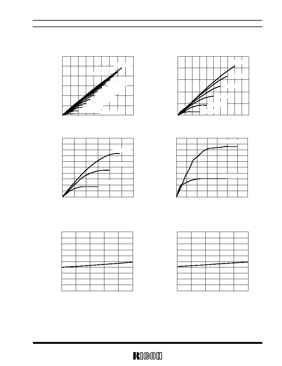
17) Output Delay Time of Release vs. Temperature
R1151N (-V
DET
=8.0V)
R1151N (-V
DET
=1.7V)
3.00
2.75
1.75
1.00
0.50
External Capacitance=220pF
Temperature Topt(
∞C)
Output Delay Time of Release tPLH(ms)
-40
10
35
85
-15
60
0.75
1.50
1.25
2.50
2.25
2.00
3.00
2.75
1.75
1.00
0.50
External Capacitance=220pF
Temperature Topt(
∞C)
Output Delay Time of Release tPLH(ms)
-40
10
35
85
-15
60
0.75
1.50
1.25
2.50
2.25
2.00

R1151N
24
18) Output Delay Time of Release vs. External Capacitance for CD pin (Topt=25∞C)
R1151N (-V
DET
=8.0V)
R1151N (-V
DET
=1.7V)
100
10
1
0.1
External Capacitance for CD pin CD(pF)
Output Delay Time of Release tPLH(ms)
10
100
1000
100
10
1
0.1
External Capacitance for CD pin CD(pF)
Output Delay Time of Release tPLH(ms)
10
100
1000
19) Output Delay Time of Detect vs. External Capacitance for CD pin (Topt=25∞C)
R1151N (-V
DET
=8.0V)
R1151N (-V
DET
=4.2V)
10
1
External Capacitance for CD pin CD(pF)
Output Delay Time of Detect tPHL
(
µ
s)
10
100
1000
10
1
External Capacitance for CD pin CD(pF)
Output Delay Time of Detect tPHL
(
µ
s)
10
100
1000
R1151N (-V
DET
=2.9V)
R1151N (-V
DET
=1.7V)
10
1
External Capacitance for CD pin CD(pF)
Output Delay Time of Detect tPHL
(
µ
s)
10
100
1000
10
1
External Capacitance for CD pin CD(pF)
Output Delay Time of Detect tPHL
(
µ
s)
10
100
1000

R1151N
25
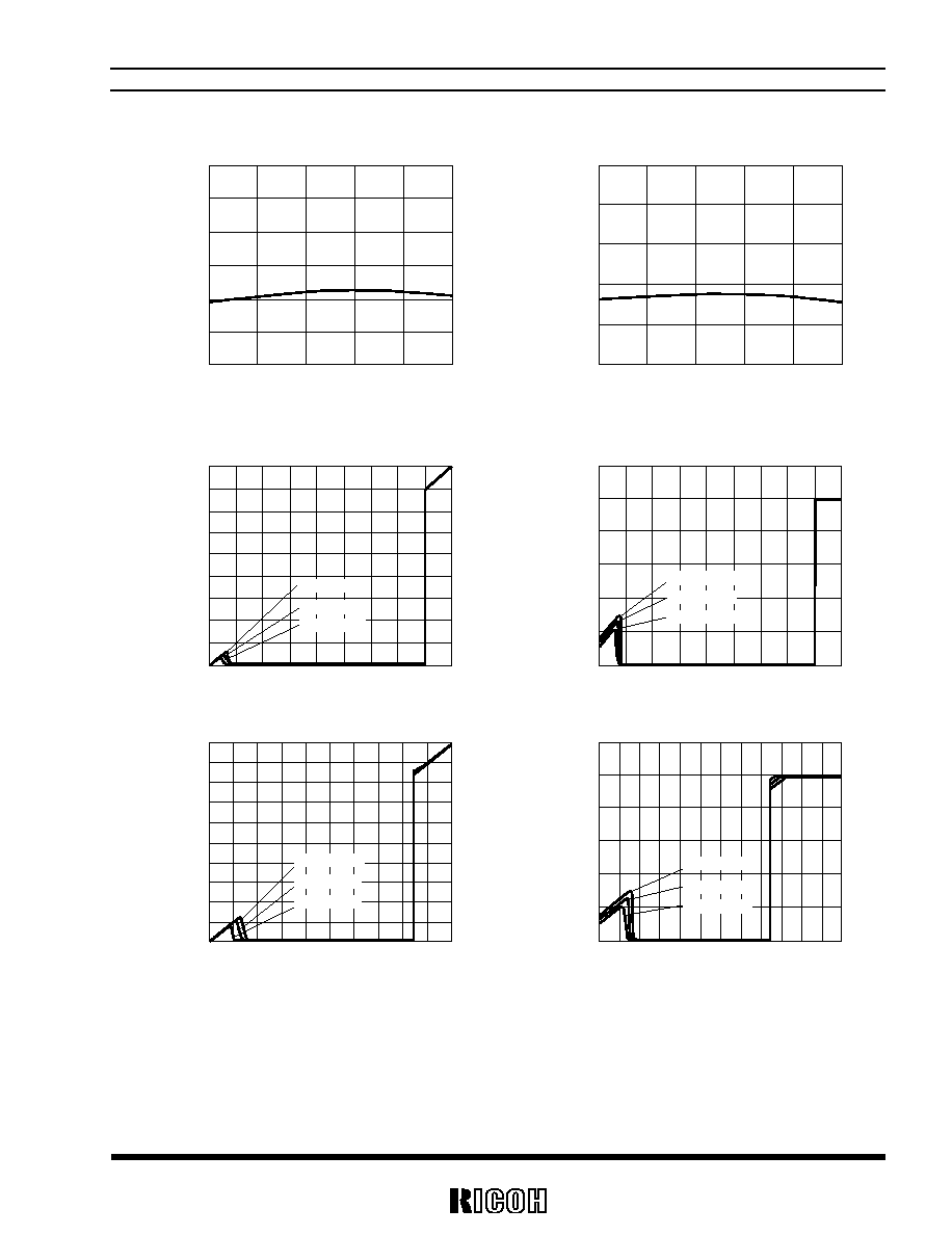
Calculation of Output Delay Time of Release
tPLH(s)=1.83◊C/(300◊10
-9
)
tPHL vs. Capacitance
30
25
0
External Capacitance for CD pin (pF)
0
2000
Released Delay Time tPLH(ms)
1000
4000
3000
5000
20
15
10
5
Measured value
Calculated value
For Stable Operation
Phase Compensation
In these ICs, phase compensation is externally made for securing stable operation even if the load current is varied.
For this purpose, be sure to use a capacitor for the output pin with good frequency characteristics and ESR (Equivalent
Series Resistance) of which is in the range described as follows:
R1151NxxxxC
V
IN
I
OUT
EXT
V
OUT
GND
V
IN
S.A.
V
DET
CD
Spectrum
Analyser
Ceramic
Capacitance
10
µF
Ceramic
Capacitor
4.7
µF
ESR
Measuring Circuit for white noise; R1151NxxxC
The relations between I
OUT
(Output Current) and ESR of Output Capacitor are shown below. The conditions when the
white noise level is under 40µV (Avg.) are marked as the hatched area in the graph.
<Measurement conditions>
(1) V
IN
=V
OUT
+1V
(2) Frequency band: 10Hz to 1MHz
(3) Temperature: 25∞C
(4) C
OUT
: Ceramic 10µF; ESR=0.075 (10kHz)

R1151N
26
VR=2.5V (2SA1441)
VR=9.0V (2SA1441)
100
10
1
0.1
0.01
Output Current I
OUT
(mA)
0
250 300 350
50 100 150 200
500
Equiv
alent Ser
ies Resistance ESR (
)
400 450
100
10
1
0.1
0.01
Output Current I
OUT
(mA)
0
250 300 350
50 100 150 200
500
Equiv
alent Ser
ies Resistance ESR (
)
400 450
VR=2.5V (2SB703)
VR=9.0V (2SB703)
100
10
1
0.1
0.01
Output Current I
OUT
(mA)
0
250 300 350
50 100 150 200
500
Equiv
alent Ser
ies Resistance ESR (
)
400 450
100
10
1
0.1
0.01
Output Current I
OUT
(mA)
0
250 300 350
50 100 150 200
500
Equiv
alent Ser
ies Resistance ESR (
)
400 450
VR=2.5V (2SB940)
VR=9.0V (2SB940)
100
10
1
0.1
0.01
Output Current I
OUT
(mA)
0
250 300 350
50 100 150 200
500
Equiv
alent Ser
ies Resistance ESR (
)
400 450
100
10
1
0.1
0.01
Output Current I
OUT
(mA)
0
250 300 350
50 100 150 200
500
Equiv
alent Ser
ies Resistance ESR (
)
400 450