 | –≠–ª–µ–∫—Ç—Ä–æ–Ω–Ω—ã–π –∫–æ–º–ø–æ–Ω–µ–Ω—Ç: R1171S | –°–∫–∞—á–∞—Ç—å:  PDF PDF  ZIP ZIP |

2000mA/1500mA LDO REGULATOR
R1171x SERIES
1
OUTLINE
The R1171x Series are CMOS-based positive voltage regulator ICs. The R1171x Series have features of low
dropout voltage, high output voltage accuracy, low consumption current. Each of these ICs consists of a voltage
reference unit, an error amplifier, resistor net for setting output voltage, a current limit circuit at short mode, a
chip enable circuit, and thermal-shunt circuit. The output voltage of R1171 is fixed in the IC.
Low consumption current by the merit of CMOS process and built-in transistors with low ON-resistance make
low dropout voltage and chip enable function prolongs the battery life. These regulators are remarkable
improvement on the current regulators in terms of input transient response, and load transient response.
Thus, the R1171x Series are suitable for various power sources.
Since the packages for these ICs are high wattage HSOP-6J package, TO252-5L(Under Development), high
density mounting of the ICs on boards is possible.
FEATURES
∑
Low Supply Current...................................................... Typ. 130
µ
A
∑
Low Standby Current.................................................... Typ. 0.1
µ
A
∑
Output Current.............................................................. Min. 2000mA (V
IN
=
V
OUT
+
1.0V, R1171JxxxC/D)
............................................................................................................................. (Under Development)
...................................................................................... Min. 1500mA (V
IN
=
V
OUT
+
1.0V, R1171SxxxA/B)
∑
Output Voltage.............................................................. Stepwise setting with a step of 0.1V in the range of
1.5V to 1.70V for A/B versions, 1.8V to 5.0V for C/D
versions.
∑
High Output Voltage Accuracy......................................
±
2.0%
∑
Low Dropout Voltage .................................................... Typ. 0.09V (V
OUT
=
3.0V, I
OUT
=
300mA)
∑
Line Regulation ............................................................ Typ. 0.05%/V
∑
Packages...................................................................... HSOP-6J, TO252-5L(Under Development)
∑
Built-in Current Limit Circuit
∑
Built-in Thermal Shutdown Circuit
∑
Low Temperature-drift Coefficient of Output Voltage ... Typ.
±
100ppm/
∞
C
∑
Ceramic capacitor for phase compensation................. Cin= Cout= Ceramic 10
µ
F (Vout<1.8V)
...................................................................................... Cin= Cout= Ceramic 4.7
µ
F (Vout
1.8V)
APPLICATIONS
∑
Local Power source for Notebook PC.
∑
Local Power source for portable appliances, cameras, and videos.
∑
Local Power source for equipment of battery-use.
∑
Local Power source for home appliances.
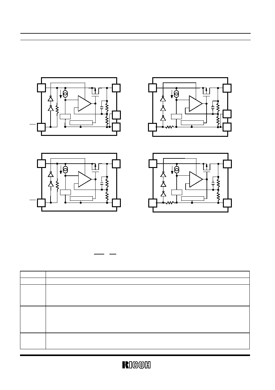
R1171x
2
BLOCK DIAGRAMS
SELECTION GUIDE
The output voltage, the chip-enable polarity, the taping type can be selected at the user's request. The
selection can be made with the part number as follows;
R1171x xx1x-xx
Part Number
a
b
c
d
Code Contents
a
Package Type; S: HSOP-6J, J: TO252-5L(Under Development)
b
Designation of Output Voltage (V
OUT
)
Stepwise setting with 0.1V increment in the range from 1.5V to 5.0V(A/B version), from 1.8V to
5.0V(C/D version: Under Development) "Exception" 2.85V type: R1171x281x5-xx, 1.85V Type:
R1171x181x5
c
Designation of option;
A: Built-in Chip Enable Circuit, Active at "L" (Output Current: Min. 1500mA)
B: Built-in Chip Enable Circuit, Active at "H" (Output Current: Min. 1500mA)
C: Built-in Chip Enable Circuit, Active at "L" (Output Current: Min. 2000mA)*Under Development
D: Built-in Chip Enable Circuit, Active at "H" (Output Current: Min. 2000mA)*Under Development
d
Designation of Taping Type;
E2 (HSOP-6J) (Refer to Taping Specifications)
TO252-5L : unfixed
V
DD
V
OUT
GND
6
3
5
1
Vref
+
-
CE
z
R1171SxxxA
Current Limit
2
GND
V
DD
V
OUT
GND
6
3
5
1
Vref
+
-
CE
z
R1171SxxxB
Current Limit
2
GND
V
DD
V
OUT
GND
5
2
3
1
Vref
+
-
CE
q
R1171JxxxC (Under Development)
Current Limit
V
DD
V
OUT
GND
5
2
3
1
Vref
+
-
CE
q
R1171JxxxD(Under Development)
Current Limit

R1171x
3
s
PIN CONFIGURATION
z HSOP-6J
TO252-5L (Under Development)
1
2
3
6
5
4
1
2
3
4
5
PIN DESCRIPTION
z HSOP-6J
Pin No
Symbol
Description
1 V
OUT
Voltage Regulator Output Pin
2 GND
Ground
Pin
3
CE or CE
Chip Enable Pin
4
NC
No Connection
5 GND
Ground
Pin
6 V
DD
Input
Pin
z TO252-5L (Under Development)
Pin No
Symbol
Description
1 V
OUT
Voltage Regulator Output Pin
2
CE or CE
Chip Enable Pin
3 GND
Ground
Pin
4 NC
No
Connection
5 V
DD
Input
Pin
R1171x
4
ABSOLUTE MAXIMUM RATINGS
Symbol Item
Rating
Unit
V
IN
Input Voltage
7.0
V
V
CE
Input Voltage ( CE or CE Input Pin)
-
0.3 ~ V
IN
+
0.3
V
V
OUT
Output Voltage
-
0.3 ~ V
IN
+
0.3
V
I
OUT
Output Current
3.5
A
P
D
Power Dissipation
Internally limited
Topt
Operating Temperature
-
40 ~ 85
∞
C
Tstg
Storage Temperature
-
55 ~ 125
∞
C
ELECTRICAL CHARACTERISTICS
R1171xxxxA
Topt
=
25
∞
C
Symbol Item
Conditions
Min.
Typ.
Max.
Unit
V
IN
Input
Voltage
2.1
6.0 V
I
SS1
Supply
Current1
V
IN
-
V
OUT
=
1.0V
V
CE
=
GND
130
320
µ
A
Istb Standby
Current
V
IN
-
V
OUT
=
1.0V
V
IN
=
V
CE
0.1 2.0
µ
A
V
OUT
Output
voltage
V
IN
-
V
OUT
=
1.0V
I
OUT
=
200mA
◊
0.98
◊
1.02
V
I
OUT1
Output
Current
V
IN
-
V
OUT
=
1.0V
1500
mA
V
OUT
/
I
OUT
Load regulation
V
IN
-
V
OUT
=
1.0V
1mA
<
=
I
OUT
<
=
300mA
30
60
mV
V
DIF
Dropout
Voltage
I
OUT
=
300mA
V
OUT
/
V
IN
Line regulation
I
OUT
=
200mA
RR Ripple
Rejection
f
=
1kHz, Ripple
0.5Vp
-
p
Refer to Electrical Characteristics by
Output Voltage
V
OUT
/
T
Output Voltage
Temperature Coefficient
I
OUT
=
10mA
-
40
∞
C
<
=
Topt
<
=
85
∞
C
±
100
ppm/
∞
C
I
LIM
Short Current Limit
V
OUT
=
0V
200
mA
R
PU
Pull-up resistancefor CE pin
2.5
5.0
10.0
M
V
CEH
CE Input Voltage "H"
1.2
V
IN
V
V
CEL
CE Input Voltage "L"
0.00
0.25
V
T
TSD
Thermal Shutdown
Detector Threshold
Temperature
Junction Temperature
150
∞
C
T
TSR
Thermal Shutdown
Released Temperature
Junction Temperature
120
∞
C

R1171x
5
∑
R1171xxxxB
Topt
=
25
∞
C
Symbol Item
Conditions
Min.
Typ.
Max.
Unit
V
IN
Input Voltage
2.1 6.0 V
I
SS1
Supply Current1
V
IN
-
V
OUT
=
1.0V V
CE
=
V
IN
150
320
µ
A
Istb
Standby Current
V
IN
-
V
OUT
=
1.0V
V
CE
=
GND
0.3
1.0
µ
A
V
OUT
Reference Voltage for
Adjustable Voltage Regulator
V
IN
-
V
OUT
=
1.0V
I
OUT
=
200mA
◊
0.98
◊
1.02
V
I
OUT1
Output Current
V
IN
-
V
OUT
=
1.0V
1500
mA
V
OUT
/
I
OUT
Load regulation
V
IN
-
V
OUT
=
1.0V
1mA
<
=
I
OUT
<
=
300mA
30 60
mV
V
DIF
Dropout Voltage
I
OUT
=
300mA
V
OUT
/
V
IN
Line regulation
I
OUT
=
200mA
RR Ripple
Rejection
f
=
1kHz, Ripple 0.5Vp
-
p
Refer to Electrical
Characteristics by Output
Voltage Table
V
OUT
/
T
Output Voltage
Temperature Coefficient
-
40
∞
C
<
=
Topt
<
=
85
∞
C
±
100
ppm/
∞
C
I
LIM
Short Current Limit
V
OUT
=
0V
200 mA
R
PU
Pull-down resistance
for CE pin
2.5 5.0 10.0 M
V
CEH
CE Input Voltage "H"
1.2 V
IN
V
V
CEL
CE Input Voltage "L"
0.00 0.25 V
T
TSD
Thermal Shutdown
Detector Threshold Temperature
Junction Temperature
150
∞
C
T
TSR
Thermal Shutdown
Released Temperature
Junction Temperature
120
∞
C
R1171xxxxC (Under Development)
Topt
=
25
∞
C
Symbol Item
Conditions
Min.
Typ.
Max.
Unit
V
IN
Input
Voltage
2.1
6.0 V
I
SS1
Supply Current 1
V
IN
-
V
OUT
=
1.0V
V
CE
=
GND
130
320
µ
A
Istb Standby
Current
V
IN
-
V
OUT
=
1.0V
V
IN
=
V
CE
0.1 2.0
µ
A
V
OUT
Output
voltage
V
IN
-
V
OUT
=
1.0V
I
OUT
=
200mA
◊
0.98
◊
1.02
V
I
OUT1
Output
Current
V
IN
-
V
OUT
=
1.0V
2000
mA
V
OUT
/
I
OUT
Load regulation
V
IN
-
V
OUT
=
1.0V
1mA
<
=
I
OUT
<
=
300mA
30 60
mV
V
DIF
Dropout
Voltage
I
OUT
=
300mA
V
OUT
/
V
IN
Line regulation
I
OUT
=
200mA
RR Ripple
Rejection
f
=
1kHz, Ripple 0.5Vp
-
p
Refer to Electrical
Characteristics by Output
Voltage
V
OUT
/
T
Output Voltage
Temperature Coefficient
I
OUT
=
10mA
-
40
∞
C
<
=
Topt
<
=
85
∞
C
±
100
ppm/
∞
C
I
LIM
Short Current Limit
V
OUT
=
0V
200 mA
R
PU
Pull-up resistancefor CE pin
2.5
5.0
10.0
M
V
CEH
CE Input Voltage "H"
1.2
V
IN
V

R1171x
6
V
CEL
CE Input Voltage "L"
0.00
0.25
V
T
TSD
Thermal Shutdown
Detector Threshold Temperature
Junction Temperature
150
∞
C
T
TSR
Thermal Shutdown
Released Temperature
Junction Temperature
120
∞
C
R1171xxxxD (Under Development)
Topt
=
25
∞
C
Symbol Item
Conditions
Min.
Typ.
Max.
Unit
V
IN
Input voltage
2.1 6.0 V
I
SS1
Supply Current1
V
IN
-
V
OUT
=
1.0V V
CE
=
V
IN
130
320
µ
A
Istb
Standby Current
V
IN
-
V
OUT
=
1.0V
V
CE
=
GND
0.1
2.0
µ
A
V
OUT
Reference Voltage for
Adjustable Voltage Regulator
V
IN
-
V
OUT
=
1.0V
I
OUT
=
200mA
◊
0.98
◊
1.02
V
I
OUT1
Output Current
V
IN
-
V
OUT
=
1.0V
2000
mA
V
OUT
/
I
OUT
Load regulation
V
IN
-
V
OUT
=
1.0V
1mA
<
=
I
OUT
<
=
300mA
30 60
mV
V
DIF
Dropout Voltage
I
OUT
=
300mA
V
OUT
/
V
IN
Line regulation
I
OUT
=
200mA
RR Ripple
Rejection
f
=
1kHz, Ripple 0.5Vp
-
p
Refer to Electrical Characteristics
by Output Voltage
V
OUT
/
T
Output Voltage
Temperature Coefficient
I
OUT
=
10mA
-
40
∞
C
<
=
Topt
<
=
85
∞
C
±
100
ppm/
∞
C
I
LIM
Short Current Limit
V
OUT
=
0V
200 mA
R
PU
Pull-down resistance
for CE pin
2.5 5.0 10.0 M
V
CEH
CE Input Voltage "H"
1.2 V
IN
V
V
CEL
CE Input Voltage "L"
0.00 0.25 V
T
TSD
Thermal Shutdown
Detector Threshold Temperature
Junction Temperature
150
∞
C
T
TSR
Thermal Shutdown
Released Temperature
Junction Temperature
120
∞
C
∑
Electrical Characteristics by Output Voltage (Topt=25
∞
∞
∞
∞
C)
Dropout Voltage (V)
Output Voltage V
OUT
(V)
Typ.
Max.
1.5V
V
OUT
<
1.6
0.16 0.35
1.6V
V
OUT
<
1.7
0.14 0.32
1.7
V
OUT
<
1.8
0.13 0.28
1.8
V
OUT
<2
.0
0.12 0.24
2.0
V
OUT
<2
.5
0.10 0.21
2.0
V
OUT
5.0
0.09 0.18
Line Regulation (%/V)
Output Voltage V
OUT
(V)
Condition Typ.
Max.
1.5V
V
OUT
<
1.6 2.1V
V
IN
6.0V
1.6
V
OUT
5.0 V
OUT
+0.5V
V
IN
6.0V
0.05 0.30

R1171x
7
Line Regulation (%/V)
Output Voltage V
OUT
(V)
Condition Typ.
1.5V
V
OUT
<4
.7
V
IN
-V
OUT
=1.0V
4.7
V
OUT
5.0
V
IN
=5.75V
50
TEST CIRCUITS
5
4
1
2
V
OUT
GND
CE
V
DD
R1171xxxxB Series
IN
OUT
Cout
1
4
5
2
V
OUT
GND
CE
V
DD
IN
OUT
Standard Test Circuit
1
4
5
2
V
OUT
GND
CE
V
DD
IN
OUT
1
4
5
2
V
OUT
GND
CE
V
DD
IN
OUT
Supply Current Test Circuit
I
SS
Iout
P.G
Iout
I1
I2
Cin
Cin
Cout
Cout
Cout
R1171xxxxB Series
R1171xxxxB
Series
R1171xxxxB
Series
Cin
Test Circuit for Ripple Rejection,
Test Circuit for Load Transient Response
Input Transient Response

R1171x
8
Technical Notes on External Components and Typical Application
Phase Compensation
In these ICs, phase compensation is made with the output capacitor for securing stable operation even if the
load current is varied. For this purpose, use a capacitor with the capacitance range from 4.7µF to 10.0
µ
F, as C
L
.
In case that using a tantalum capacitor and the ESR of the tantalum capacitor is too large, unstable operation
may result. Fully evaluation is necessary for the whole circuit with considering the frequency characteristic.
Mounting on PCB
Make V
DD
and GND lines sufficient. If their impedance is high, large current may flow and the pick-up noise or
unstable operation may result. Therefore use a capacitor with a capacitance range from 4.7
µ
F to 10µF between
V
DD
pin and GND pin as close as possible.
Further, set an output capacitor between V
OUT
pin and GND pin for phase compensation as close as possible.
(Refer to the example of typical application)
R1171Sxx1B Typical Application
IN
OUT
V
DD
CE
GND
V
OUT
CI
CL
R1171Sxx1B
1.5V
V
OUT<
1.8V: CI=10
µ
F(Ceramic), CL=10
µ
F(Ceramic)
1.8V
V
OUT
5.0V: CI=4.7
µ
F(Ceramic), CL=4.7
µ
F(Ceramic)
Output Short Protection Function
In the R1171 Series, the output short protection function is built in, further, if the output is short to the GND or
other voltage line, the chip inside is heating, as a result, in case that the junction temperature becomes equal or
more than 150
∞
C(Typ.), the built-in thermal shutdown circuit works. If the junction temperature becomes equal
or more than 150
∞
C(Typ.), the IC is protected by the output short protection circuit and the thermal shutdown
circuit.
R1171x
9
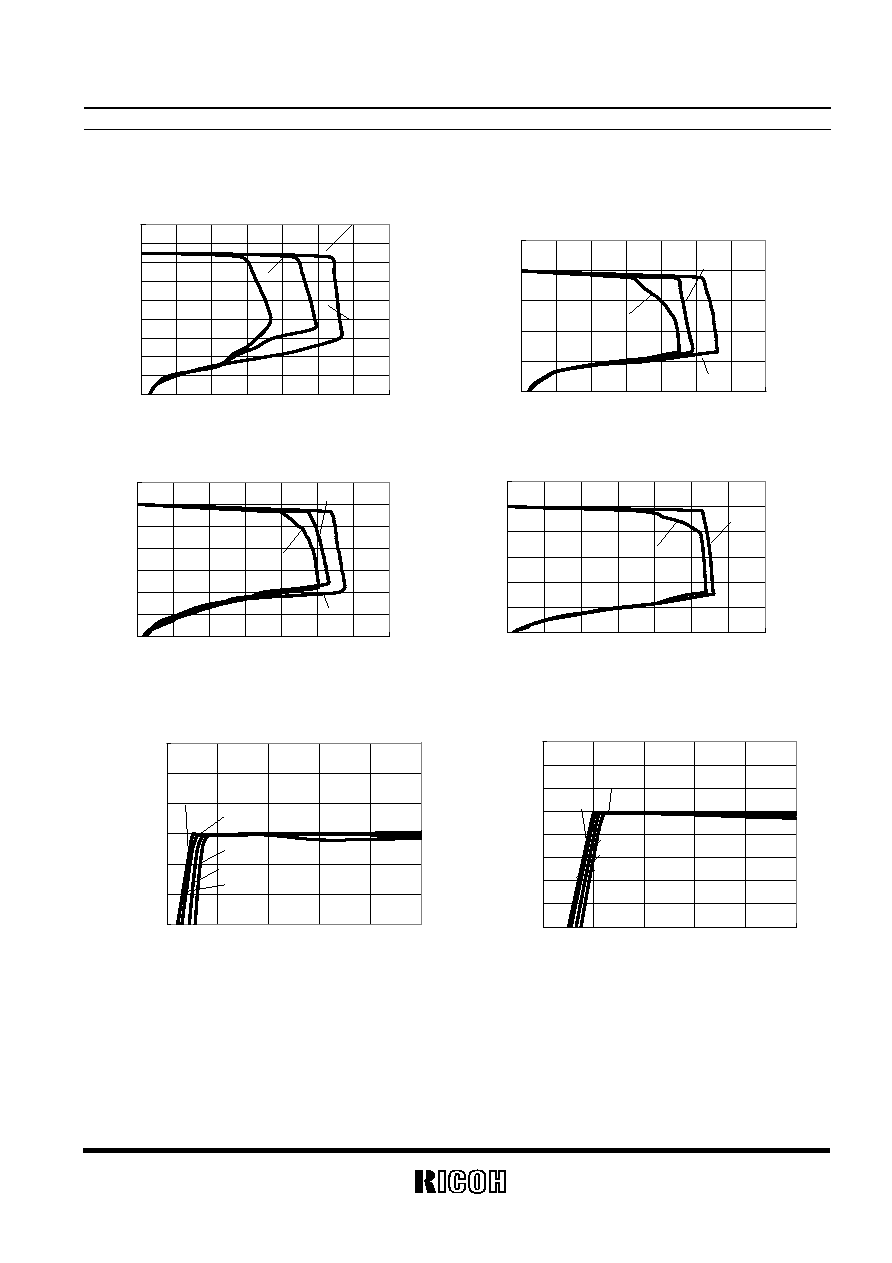
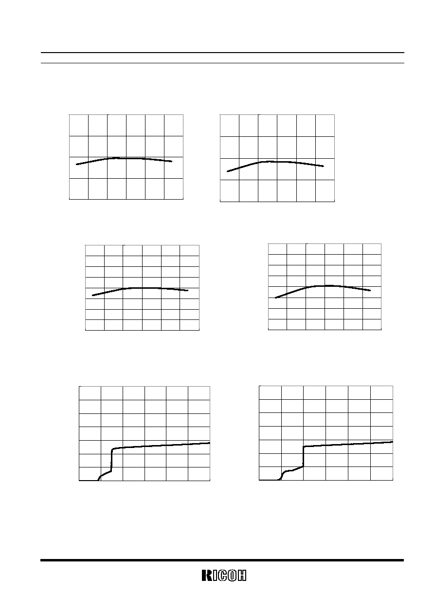
TYPICAL CHARACTERISTICS
1) Output Voltage vs. Output Current (Topt=25
∞
∞
∞
∞
C)
R1171S151x
0
0.2
0.4
0.6
0.8
1
1.2
1.4
1.6
1.8
0
500 1000 1500 2000 2500 3000 3500
Output Current I
OUT
(mA)
O
u
tput Voltage V
OU
T
(V)
R1171S201x
0
0.5
1
1.5
2
2.5
0
500 1000 1500 2000 2500 3000 3500
Output Current I
OUT
(mA)
Out
put
Vol
t
age V
OUT
(V
)
R1171S301x
0
0.5
1
1.5
2
2.5
3
3.5
0
500 1000 1500 2000 2500 3000 3500
Output Current I
OUT
(mA)
O
u
tput Voltage V
OUT
(V)
R1171S501x
0
1
2
3
4
5
6
0
500 1000 1500 2000 2500 3000 3500
Output Current I
OUT
(mA)
O
u
tput Voltage V
OUT
(V)
2) Output Voltage vs. Input Voltage (Topt
=
=
=
=
25∞C)
R1171x151B
1.2
1.3
1.4
1.5
1.6
1.7
1.8
1
2
3
4
5
6
Input Voltage VIN(V)
Out
put
V
o
l
t
age V
O
UT(V
)
R1171x201B
1.5
1.6
1.7
1.8
1.9
2.0
2.1
2.2
2.3
1
2
3
4
5
6
Input Voltage VIN(V)
Out
put
V
o
l
t
age V
O
UT(V
)
I
OUT
=500mA
I
OUT
=300mA
I
OUT
=100mA
I
OUT
=10mA
I
OUT
=1mA
I
OUT
=500mA
I
OUT
=300mA
I
OUT
=100mA
I
OUT
=10mA
I
OUT
=1mA
V
IN
=2V
V
IN
=2.5V
V
IN
=3.5V
V
IN
=2.5V
V
IN
=3V
V
IN
=4V
V
IN
=3.5V
V
IN
=4V
V
IN
=5V
V
IN
=5.5V
V
IN
=6V
R1171x
10
R1171x301B
2.5
2.6
2.7
2.8
2.9
3.0
3.1
3.2
3.3
2
3
4
5
6
Input Voltage VIN(V)
Out
put
V
o
l
t
age V
O
UT(V
)
R1171x501B
4.5
4.6
4.7
4.8
4.9
5.0
5.1
5.2
5.3
4.0
4.5
5.0
5.5
6.0
Input Voltage VIN(V)
Out
put
V
o
l
t
age V
O
UT(V
)
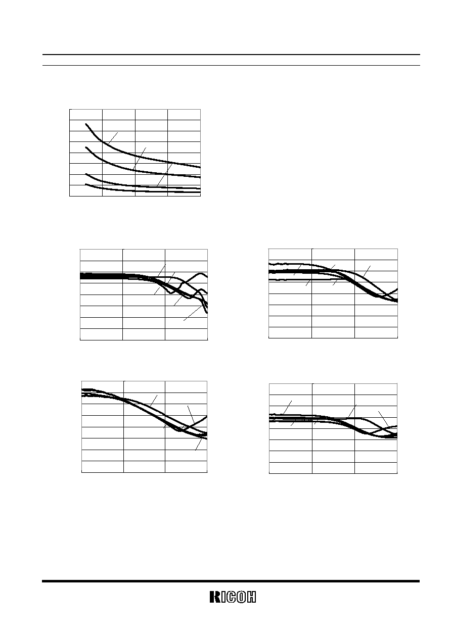
3)Dropout Voltage vs. Output Current
R1171S151x
0
0.1
0.2
0.3
0.4
0.5
0.6
0.7
0.8
0.9
1
0
250
500
750
1000 1250 1500
Output Current I
OUT
(mA)
D
r
opout V
o
ltage V
DIF
(V
)
R1171S201x
0
0.1
0.2
0.3
0.4
0.5
0.6
0.7
0.8
0.9
1
0
250
500
750
1000
1250
1500
Output Current I
OUT
(mA)
Dropout
V
o
l
t
age V
DIF
(V
)
R1171S301x
0
0.1
0.2
0.3
0.4
0.5
0.6
0.7
0.8
0.9
1
0
250
500
750
1000 1250 1500
Output Current I
OUT
(mA)
D
r
opout V
o
ltage V
DIF
(V
)
R1171S501x
0
0.1
0.2
0.3
0.4
0.5
0.6
0.7
0.8
0.9
1
0
250
500
750
1000
1250
1500
Output Current I
OUT
(mA)
Dropout
V
o
l
t
age V
DIF
(V
)
IOUT=500mA
I
OUT
=300mA
I
OUT
=100mA
I
OUT
=10mA
I
OUT
=1mA
I
OUT
=500mA
I
OUT
=300mA
I
OUT
=300mA
I
OUT
=10mA
I
OUT
=1mA
85
∞
C
25
∞
C
-40
∞
C
85
∞
C
25
∞
C
-40
∞
C
85C
25
∞
C
-40
∞
C
85
∞
C
25
∞
C
-40
∞
C
R1171x
11
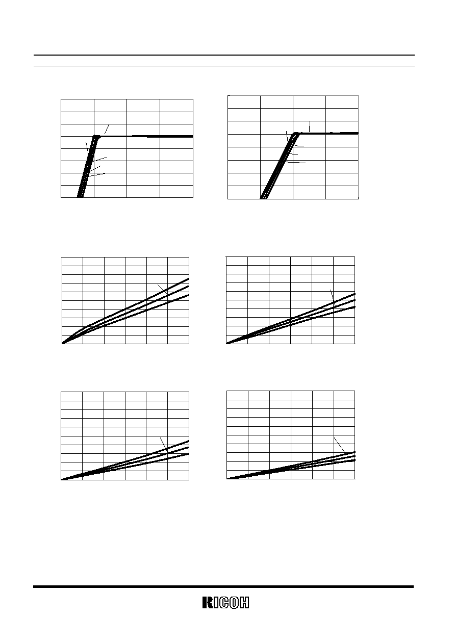
4) Output Voltage vs. Temperature
R1171x151B
V
IN
=2.5V, I
OUT
=200mA
1.40
1.45
1.50
1.55
1.60
-50
-25
0
25
50
75
100
Temperature Topt(
∞
C)
Out
put
V
o
l
t
age V
OU
T
(V
)
R1171x201B
V
IN
=3.0V,I
OUT
=200mA
1.90
1.95
2.00
2.05
2.10
-50
-25
0
25
50
75
100
Temperature Topt(
∞
C)
Out
put
V
o
l
t
age V
OU
T
(V
)
R1171x301B
V
IN
=4.0V, I
OUT
=200mA
2.80
2.85
2.90
2.95
3.00
3.05
3.10
3.15
3.20
-50
-25
0
25
50
75
100
Temperature Topt(
∞
C)
Out
put
V
o
l
t
age V
OU
T
(V
)
R1171x501B
V
IN
=5.0V, I
OUT
=200mA
4.80
4.85
4.90
4.95
5.00
5.05
5.10
5.15
5.20
-50
-25
0
25
50
75
100
Temperature Topt(
∞
C)
Out
put
V
o
l
t
age V
OU
T
(V
)
5) Supply Current vs. Input Voltage (Topt
=
=
=
=
25∞C)
R1171x151B
0
50
100
150
200
250
300
350
0
1
2
3
4
5
6
Input Voltage VIN(V)
S
uppl
y
Current
I
s
s
(
µ
A)
R1171x201B
0
50
100
150
200
250
300
350
0
1
2
3
4
5
6
Input Voltage VIN(V)
S
uppl
y
Current
I
s
s
(
µ
A)
R1171x
12
R1171x301B
0
50
100
150
200
250
300
350
0
1
2
3
4
5
6
Input Voltage VIN(V)
S
uppl
y
Current
I
s
s
(
µ
A)
R1171x501B
0
50
100
150
200
250
300
350
0
1
2
3
4
5
6
Input Voltage VIN(V)
S
uppl
y
Current
I
s
s
(
µ
A)
4) Supply Current vs. Temperature
R1171x151B
V
IN
=2.5V
0
50
100
150
200
250
300
350
-50
-25
0
25
50
75
100
Temperature Topt(
∞
C)
S
uppl
y
Current
I
s
s
(
µ
A)
R1171x201B
V
IN
=3.0V
0
50
100
150
200
250
300
350
-50
-25
0
25
50
75
100
Temperature Topt(
∞
C)
S
uppl
y
Current
I
s
s
(
µ
A)
R1171x301B
V
IN
=4.0V
0
50
100
150
200
250
300
350
-50
-25
0
25
50
75
100
Temperature Topt(
∞
C)
S
uppl
y
Current
I
s
s
(
µ
A)
R1171x501B
V
IN
=6.0V
0
50
100
150
200
250
300
350
-50
-25
0
25
50
75
100
Temperature Topt(
∞
C)
S
uppl
y
Current
I
s
s
(
µ
A)
R1171x
13
7) Dropout Voltage vs. Set Output Voltage (Topt
=
=
=
=
25∞C)
R1171Sxx1x
0.0
0.1
0.2
0.3
0.4
0.5
0.6
0.7
0.8
1
2
3
4
5
Set Output Voltage VSET(V)
Dropout
V
o
l
t
age V
D
I
F
(V
)
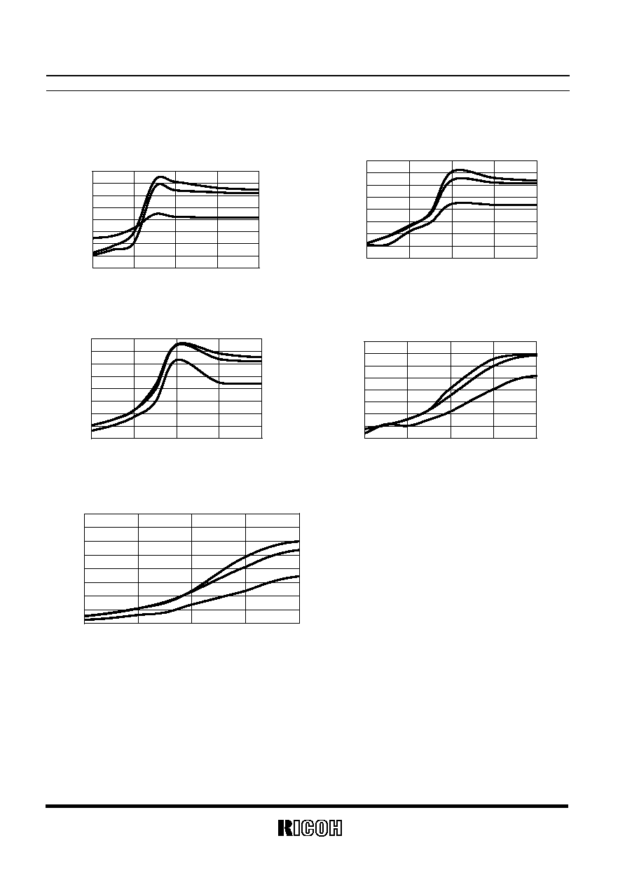
8) Ripple Rejection vs. Frequency
R1171x151B
VIN=2.5V+0.5VP-P
0
10
20
30
40
50
60
70
80
0.1
1.0
10.0
100.0
Ripple Frequency (kHz)
Ri
ppl
e Rej
e
c
t
i
on RR(dB
)
R1171x201B
VIN=3.0V+0.5VP-P
0
10
20
30
40
50
60
70
80
0.1
1.0
10.0
100.0
Ripple Frequency (kHz)
Ri
ppl
e Rej
e
c
t
i
on RR(dB
)
R1171x301B
VIN=4.0V+0.5VP-P
0
10
20
30
40
50
60
70
80
0.1
1.0
10.0
100.0
Ripple Frequency (kHz)
Ri
ppl
e Rej
e
c
t
i
on RR(dB
)
R1171x501B
VIN=5.75V+0.5VP-P
0
10
20
30
40
50
60
70
80
0.1
1.0
10.0
100.0
Ripple Frequency f(kHz)
Ri
ppl
e Rej
e
c
t
i
on RR(dB
)
I
OUT
=1mA
I
OUT
=10mA
I
OUT
=100mA
I
OUT
=200mA
I
OUT
=500mA
I
OUT
=1mA
I
OUT
=10mA
I
OUT
=100mA
I
OUT
=200mA
I
OUT
=500mA
I
OUT
=1mA
I
OUT
=10mA
I
OUT
=100mA
I
OUT
=200mA
I
OUT
=500mA
I
OUT
=1mA
I
OUT
=10mA
I
OUT
=100mA
I
OUT
=200mA
I
OUT
=500mA
I
OUT
=1500mA
I
OUT
=1000mA
I
OUT
=200mA
I
OUT
=600mA
R1171x
14
9) Ripple Rejection vs. Input Voltage
R1171x301x
I
OUT
=1mA,C
OUT
=4.7µ
F
0
10
20
30
40
50
60
70
80
3.1
3.2
3.3
3.4
3.5
Input Voltage V
IN
(V)
Ri
ppl
e Rej
e
ct
i
o
n
RR(
dB)
R1171x301x
I
OUT
=10mA,C
OUT
=4.7µ
F
0
10
20
30
40
50
60
70
80
3.1
3.2
3.3
3.4
3.5
Input Voltage V
IN
(V)
R
i
pple R
e
jection
RR(
d
B
)
R1171x301x
I
OUT
=100mA,C
OUT
=4.7µ
F
0
10
20
30
40
50
60
70
80
3.1
3.2
3.3
3.4
3.5
Input Voltage V
IN
(V)
R
i
pple R
e
jection
RR(
d
B
)
R1171x301x
I
OUT
=300mA,C
OUT
=4.7µ
F
0
10
20
30
40
50
60
70
80
3.1
3.2
3.3
3.4
3.5
Input Voltage V
IN
(V)
Ri
ppl
e Rej
e
c
t
i
o
n
RR(dB
)
R1171x301x
I
OUT
=500mA,C
OUT
=4.7µF
0
10
20
30
40
50
60
70
80
3.1
3.2
3.3
3.4
3.5
Input Voltage VIN(V)
Ri
ppl
e Rej
e
c
t
i
o
n
RR(dB
)
f=400Hz
f=1kHz
f=10kHz
f=400Hz
f=1kHz
f=10kHz
f=400Hz
f=1kHz
f=10kHz
f=400Hz
f=1kHz
f=10kHz
f=400Hz
f=1kHz
f=10kHz

R1171x
15
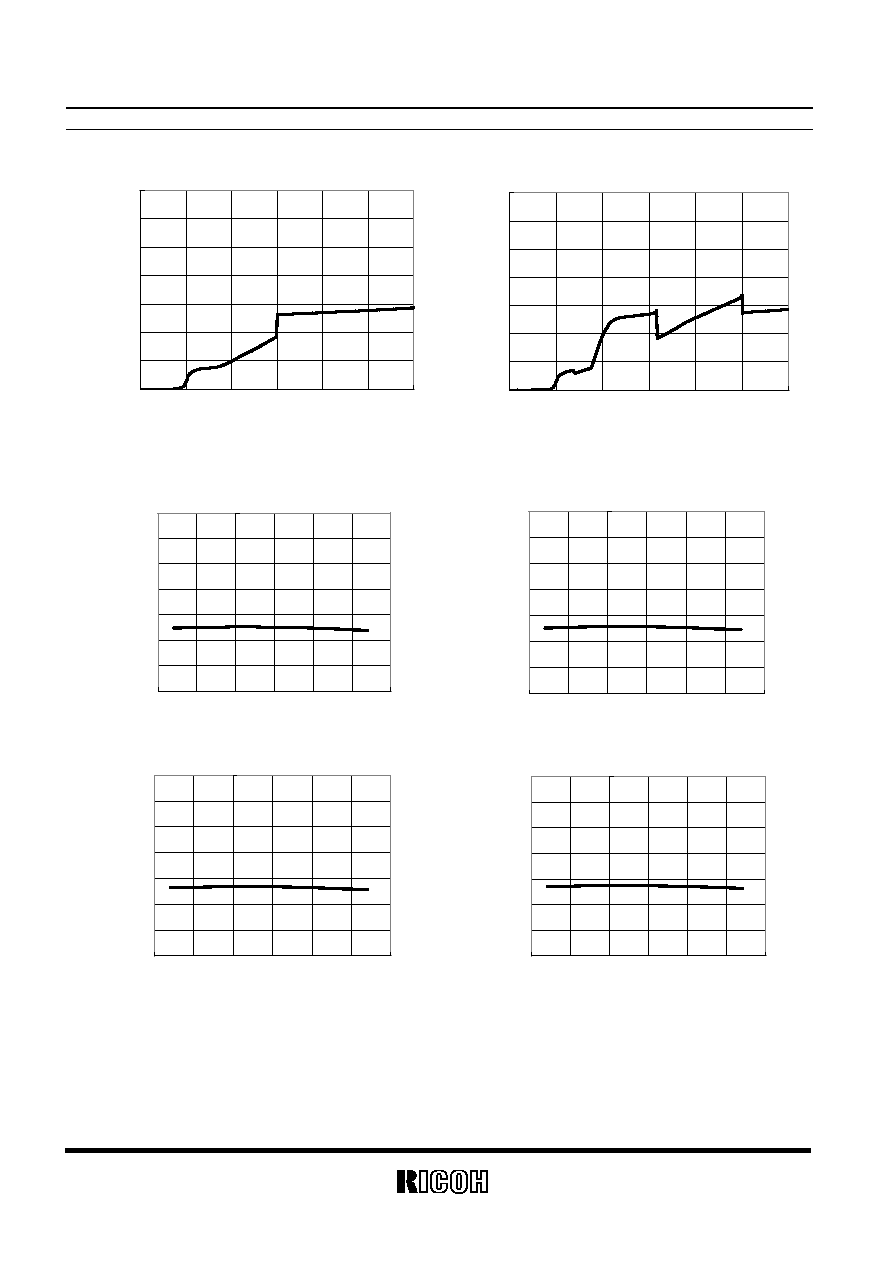
10) Input Transient Response (Topt
=
25∞C)
R1171x151B
tr=tf=5
µ
s, I
OUT
=1000mA, C
OUT
=Ceramic 10
µ
F
1.40
1.45
1.50
1.55
1.60
1.65
1.70
1.75
1.80
0
20
40
60
80
100
120
140
160
180
200
Time
T(
µ
s)
Out
put
V
o
l
t
age
V
OU
T
(V
)
0.0
0.5
1.0
1.5
2.0
2.5
3.0
3.5
4.0
I
nput
V
o
l
t
age V
IN
(V
)
R1171x301B
tr=tf=5
µ
s, I
OUT
=1000mA, C
OUT
=Ceramic 4.7
µ
F
2.90
2.95
3.00
3.05
3.10
3.15
3.20
0
20
40
60
80
100
120
140
160
180
200
Time
T(
µ
s)
Ou
t
p
u
t
Vo
lt
a
g
e
V
OU
T
(V
)
1.0
1.5
2.0
2.5
3.0
3.5
4.0
4.5
5.0
5.5
I
nput
V
o
l
t
age V
IN
(V
)
Input Voltage
Input Voltage
R1171x201B
tr=tf=5
µ
s, I
OUT
=1000mA, C
OUT
=Ceramic 4.7
µ
F
1.90
1.95
2.00
2.05
2.10
2.15
2.20
2.25
2.30
0
20
40
60
80
100
120
140
160
180
200
Time
T(
µ
s)
O
u
tput Voltage
V
OUT
(V)
0.5
1.0
1.5
2.0
2.5
3.0
3.5
4.0
4.5
I
nput
V
o
l
t
age V
IN
(V
)
Input Voltage
Output Voltage
Input Voltage
Output Voltage
Input Voltage
Output Voltage
R1171x
16
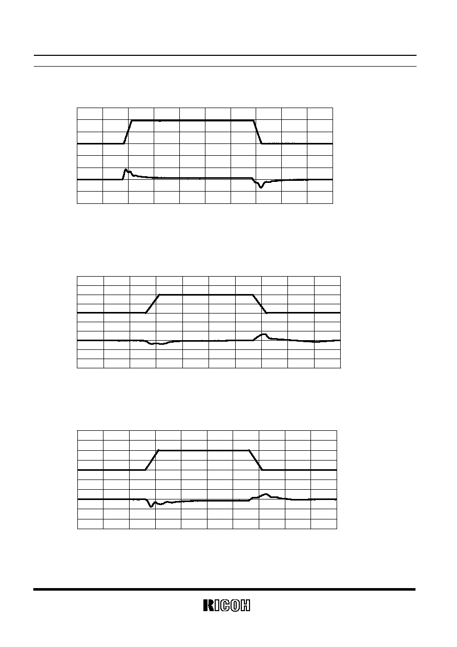
11) Load Transient Response (Topt
=
=
=
=
25∞C)
R1171x201B
tr=tf=10
µ
s, V
IN
=3.0V, C
OUT
=Ceramic 4.7
µ
F
1.85
1.90
1.95
2.00
2.05
2.10
2.15
2.20
2.25
2.30
2.35
0
20
40
60
80
100
120
140
160
180
200
Time
T (
µ
s)
Out
put
V
o
lt
age V
OUT
(V
)
-3000
-2500
-2000
-1500
-1000
-500
0
500
1000
1500
2000
Out
put
Current
I
OUT
(m
A
)
R1171x151B
tr=tf=10
µ
s, V
IN
=2.5V, COUT=Ceramic 10
µ
F
1.35
1.40
1.45
1.50
1.55
1.60
1.65
1.70
1.75
1.80
1.85
0
20
40
60
80
100
120
140
160
180
200
Time
T (
µ
s)
Output Voltag
e
V
OU
T
(
V
)
-3000
-2500
-2000
-1500
-1000
-500
0
500
1000
1500
2000
O
u
tput Current I
OUT
(
mA
)
Output Voltage
Output Current
R1171x501B
tr=tf=5
µ
s, I
OUT
=1000mA, C
OUT
=Ceramic 4.7
µ
F
4.90
4.95
5.00
5.05
5.10
5.15
5.20
5.25
5.30
0
20
40
60
80
100
120
140
160
180
200
Time
T (
µ
s)
O
u
tput V
o
ltage V
OUT
(V)
3.5
4.0
4.5
5.0
5.5
6.0
6.5
7.0
7.5
Input V
o
ltage V
IN
(V
)
Output Voltage
Output Voltage
Output Current
Output Current
Input Voltage
Output Voltage

R1171x
17
12) Stable Area (Topt
=
25
∞
C, V
IN
=
Set Output Voltage
+
1V, C
IN
=
Ceramic 10
µ
F)
As an output capacitor for this IC, Ceramic capacitor is recommendable. However, other low ESR type
capacitor can be used with this IC.
For your reference, noise level is tested with the circuit as shown above, and if the noise level is 40
µ
V or less
than 40
µ
V, the ESR values are plotted as stable area. Upper limit is described in the next four graphs, or ESR
R1171x301B
tr=tf=10
µ
s, V
IN
=4.0V, C
OUT
=Ceramic 4.7
µ
F
2.85
2.90
2.95
3.00
3.05
3.10
3.15
3.20
3.25
3.30
3.35
0
20
40
60
80
100
120
140
160
180
200
Time
T(
µ
s)
O
u
tput Voltage V
OU
T
(V)
-3000
-2500
-2000
-1500
-1000
-500
0
500
1000
1500
2000
O
u
t
p
ut
Cur
r
ent
I
OUT
(
mA
)
Output Voltage
Output Current
R1171x501B
tr=tf=10
µ
s, V
IN
=6.0V, C
OUT
=Ceramic 4.7
µ
F
4.85
4.90
4.95
5.00
5.05
5.10
5.15
5.20
5.25
5.30
5.35
0
20
40
60
80
100
120
140
160
180
200
Time T (
µ
s)
O
u
tput Voltage V
OUT
(V)
-3000
-2500
-2000
-1500
-1000
-500
0
500
1000
1500
2000
O
u
tput C
u
rrent I
OUT
(m
A)
Output Current
Output Voltage
IN
V
Cin
V
OUT
GND
CE
IN
R11
71x
xx
1
B
Cout
V
S.A.
Spectrum
Analyzer
I
OUT
ESR

R1171x
18
vs. Output Current. (Hatched area is the stable area.)
R1171S151x
0.01
0.1
1
10
100
0
250
500
750 1000 1250 1500
Output Current IOUT(mA)
ESR
(
)
C
IN
=C
OUT
=Ceramic 10µF
R1171S151x
0.01
0.1
1
10
100
0
250
500
750 1000 1250 1500
Output Current IOUT(mA)
ESR
(
)
C
IN
=C
OUT
=Ceramic 4.7µF
R1171S301x
0.01
0.1
1
10
100
0
250
500
750 1000 1250 1500
Output Current IOUT(mA)
ESR
(
)
C
IN
=C
OUT
=Ceramic 4.7µF
R1171S301x
0.01
0.1
1
10
100
0
250
500
750 1000 1250 1500
Output Current IOUT(mA)
ESR
(
)
C
IN
=COUT=Ceramic 2.2µF
R1171S501x
0.01
0.1
1
10
100
0
250
500
750 1000 1250 1500
Output Current IOUT(mA)
ESR
(
)
C
IN
=C
OUT
=Ceramic 4.7µF
R1171S501x
0.01
0.1
1
10
100
0
250
500
750 1000 1250 1500
Output Current IOUT(mA)
ESR
(
)
C
IN
=C
OUT
=Ceramic 2.2µF