 | –≠–ª–µ–∫—Ç—Ä–æ–Ω–Ω—ã–π –∫–æ–º–ø–æ–Ω–µ–Ω—Ç: R1173D | –°–∫–∞—á–∞—Ç—å:  PDF PDF  ZIP ZIP |

Super low On resistance/ Low voltage LDO
R1173x SERIES
1
OUTLINE
The R1173x Series are CMOS-based positive voltage regulator ICs. The R1173x Series have features of
super low dropout, 1A output current capability, and -3mV typical load regulation at 1A. Even the output voltage
is set at 1.5V, on resistance of internal FET is typically 0.32
. Therefore, applications that require a large current
at small dropout are suitable for the R1173x series. Low input voltage is acceptable and low output voltage can
be set. The minimum input voltage is 1.4V, and the lowest set output voltage is 0.8V. Each of these ICs consists
of a voltage reference unit, an error amplifier, resistor net for setting output voltage, a current limit circuit at
over-current, a chip enable circuit, a thermal-shutdown circuit, and so on. A stand-by mode with ultra low
consumption current can be realized with the chip enable pin. The output voltage types of R1173 are fixed one in
the IC and adjustable one (R1173x001x).
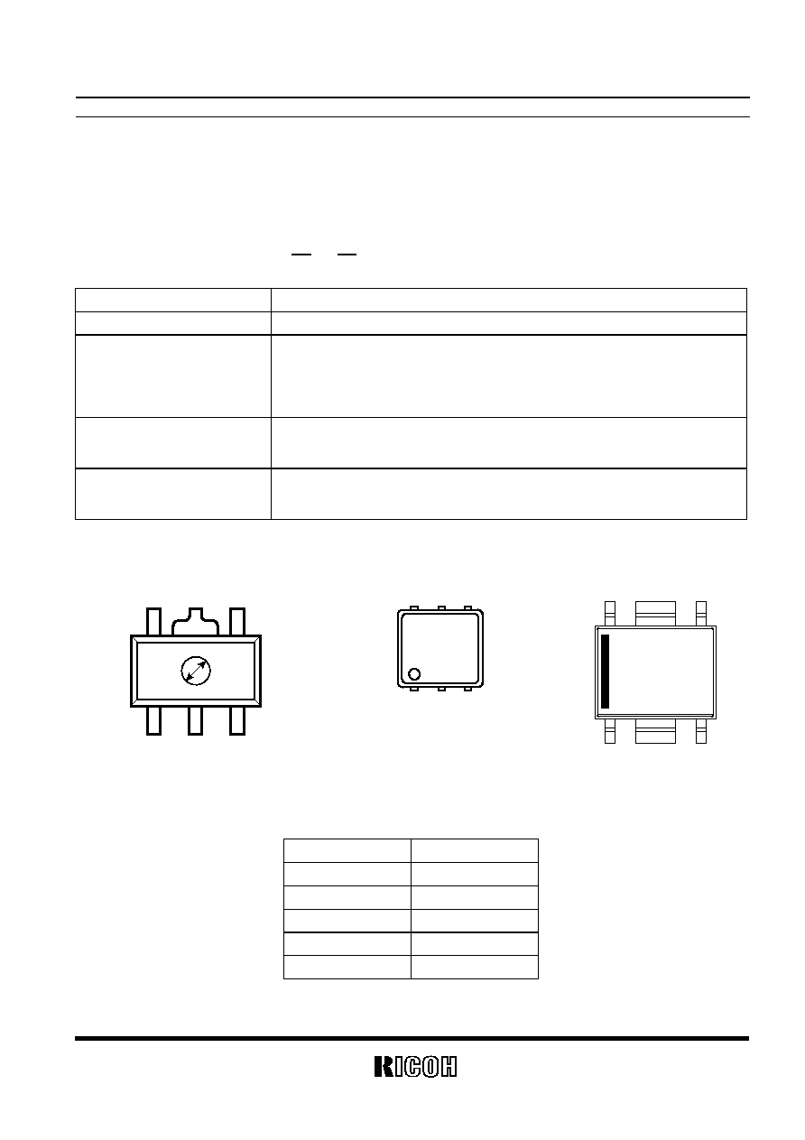
Since the packages for these ICs are the SOT-89-5 package, HSON-6, or HSOP-6J, high density mounting of
the ICs on boards is possible.
FEATURES
∑
Ultra-Low Supply Current ............................................. Typ. 60
µ
A
∑
Good Load Regulation ................................................. Typ. ≠2mV, Max.
±
15mV at I
OUT
=300mA
.....................................................................................Typ. ≠3mV at I
OUT
=1000mA
∑
Low inrush current at turning-on .................................. Typ. 500mA
∑
Minimum Input Voltage................................................. Min. 1.4V
∑
Low Standby Current.................................................... Typ. 0.1
µ
A
∑
Output Current.............................................................. Max. 1A
∑
Output Voltage ............................................Stepwise setting with a step of 0.1V in the range of
0.8V to 5.0V(Fixed output voltage type, except HSOP6J: only 0.8V to 3.5V type is available.) or
adjustable. (R1173X001X)
∑
High Power Supply Ripple Rejection .............
Typ. 70dB (V
OUT
=
3.0V)
∑
High Output Voltage Accuracy......................................
±
2.0%
∑
Low Dropout Voltage .................................................... Typ. 0.18V (V
OUT
=
3.0V, I
OUT
=1
A)
........................... Typ. 0.32V (V
OUT
=1.5V/ I
OUT
=1A)
∑
Line Regulation ............................................................ Typ. 0.05%/V
∑
Packages...................................................................... SOT-89-5, HSON-6, High power-HSOP-6J
∑
Built-in Current Limit Circuit
∑
Built-in Thermal Shutdown Circuit
∑
Low Temperature-drift Coefficient of Output Voltage ... Typ.
±
100ppm/
∞
C
∑
Output capacitors ......................................................... C
IN
=C
OUT
=Tantalum 4.7
µ
F(V
OUT
<1.0V)
...................................................................................... C
IN
=C
OUT
=Ceramic 4.7
µ
F(V
OUT
1.0V)
APPLICATIONS
∑
Local Power source for Notebook PC.
∑
Local Power source for portable communication equipments, cameras, and videos.

R1173x
2
∑
Local Power source for home appliances.
BLOCK DIAGRAMS
R1173xxx1B
R1173xxx1D
R1173X001B
R1173x001D
V
DD
V
OUT
GND
Vref
Current Limit
+
-
CE
V
DD
V
OUT
GND
Vref
Current Limit
+
-
CE
ADJ
ADJ
V
DD
V
OUT
GND
Vref
Current Limit
+
-
CE
V
DD
V
OUT
GND
Vref
Current Limit
+
-
CE
R1173x)
3
SELECTION GUIDE
The output voltage, with/without auto-discharge function, the package type, etc. can be selected at the
user's request.
The selection can be made with the part number as follows;
R1173x xx1x-xx
Part Number
a
b
c
d
Code Contents
a
Package Type; H: SOT-89-5, D: HSON-6, S: HSOP-6J
b
Designation of Output Voltage (V
OUT
)
External Setting Type: 00
Fixed Type: 08 to 50 Stepwise setting with 0.1V increment in the range from
0.8V to 5.0V, exceptions; 2.85V output: R1173x281x5-xx, 1.85V output:
R1173x181x5-xx
c
Designation of option;
B: Built-in Chip Enable Circuit, Active at "H", without auto-discharge
D: Built-in Chip Enable Circuit, Active at "H", with auto-discharge
d
Designation of Taping Type;
T1 or T2 (SOT-89-5), TR (HSON-6), E2 (HSOP-6J)
(Refer to Taping Specifications)
PIN CONFIGURATION
z SOT-89-5
z HSON-6
z HSOP-6J
5
4
1.0
1
2
3
6
5
4
1
2
3
6
5
4
1
2
3
R
PIN DESCRIPTION
z SOT-89-5
Pin No
Symbol
1
ADJ or NC
2 GND
3 CE
4 V
DD
5 V
OUT

R1173x
4
z HSON-6
Pin No
Symbol
1 V
OUT
2 V
OUT
3
ADJ or NC
4 GND
5 CE
6 V
DD
*The back side tab and tab lead is GND level.
Connect Pin1 and Pin2 as short as possible.
z HSOP-6J
Pin No
Symbol
1 V
OUT
2 GND
3
ADJ or NC
4 CE
5 GND
6 V
DD
ABSOLUTE MAXIMUM RATINGS
Symbol Item
Rating
Unit
V
IN
Input
Voltage
6.5
V
V
CE
Input Voltage (CE Input Pin)
-
0.3 ~ 6.5
V
V
OUT
Output
Voltage
-
0.3 ~ V
IN
+
0.3
V
I
OUT
Output
Current
1.4
A
P
D
Power Dissipation
Internally limited
Topt Operating
Temperature
-
40 ~ 85
∞
C
Tstg Storage
Temperature
-
55 ~ 125
∞
C

R1173x)
5
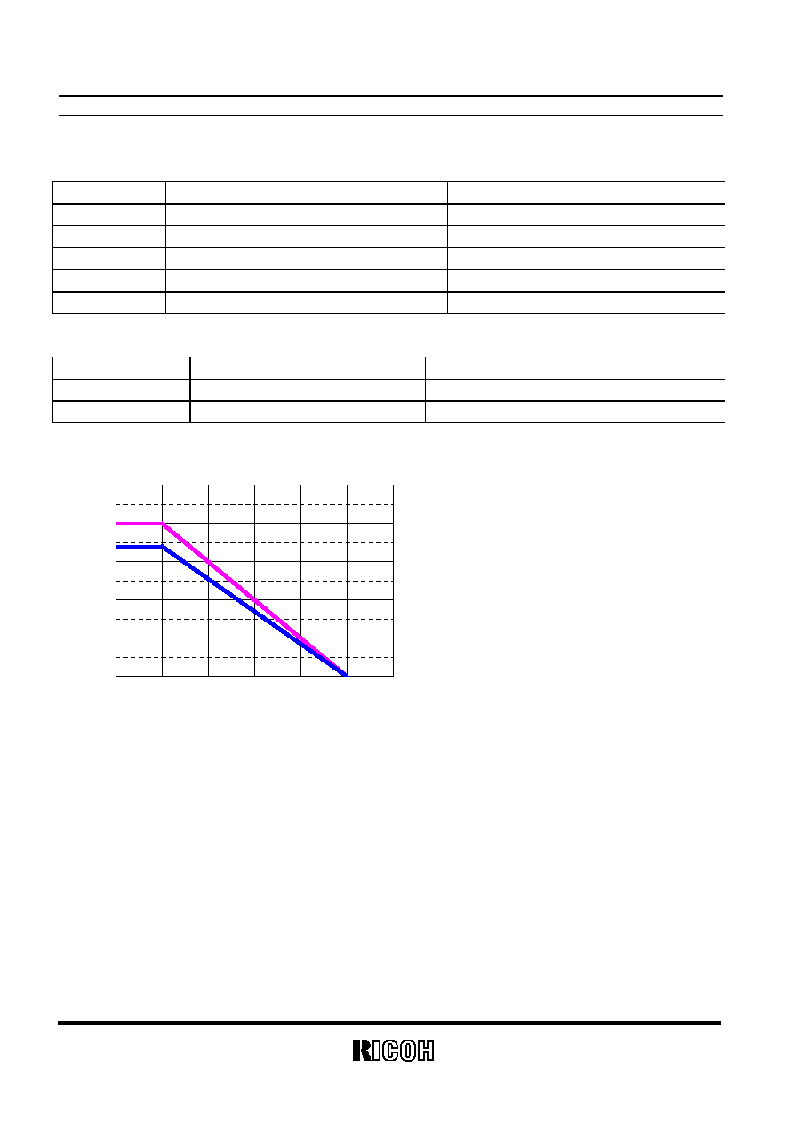
Power Dissipation (HSON-6)
Power dissipation depends on mounting conditions, the data below is an example.
∑
Measurement Conditions
∑
Mounting on board: Wind velocity=0m/s
∑
Board Material: Glass Epoxy Resin (Double Layers)
∑
Board Dimensions: 40mm*40mm*1.6mm
∑
Wiring Ratio: 50%
∑
* Measurement Result:
∑
Power Dissipation: 900mW (Topt=25
∞
C, Tjmax=125
∞
C)
∑
Thermal Resistance 111
∞
C/W
Power Dissipation (HSON-6)
0
200
400
600
800
1000
0
25
50
75
100
125
150
Temperature Topt (
∞
C)
Po
we
r
Di
s
s
i
p
a
t
i
o
n
Pd
(
m
W)
R1173x
6
Power Dissipation (HSOP-6J)
∑
Measurement Conditions
High PD Land Pattern
Standard Land Pattern
Environment
Mounting on Board (Wind velocity=0m/s)
Mounting on Board (Wind velocity=0m/s)
Board Material Glass Epoxy Resin (Double Layer type)
Glass Epoxy Resin (Double Layer type)
Board Dimensions
50mm*50mm*1.6mm 50mm*50mm*1.6mm
Wiring Ratio
90%
50%
Thermal via hole
Diameter: 0.5mm*24pieces
Diameter: 0.5mm*24pieces
Measurement Results
High PD Land Pattern
Standard Land Pattern
Power Dissipation
2000mW (Topt=25
∞
C, Tjmax=125
∞
C)
1700mW
(Topt=25
∞
C, Tjmax=125
∞
C)
Thermal Resistance
50
∞
C/W 59
∞
C/W
Power Dissipation (HSOP-6J
0
500
1000
1500
2000
2500
0
25
50
75
100
125
150
Temperature Topt(
∞
C)
Po
we
r
Di
s
s
i
p
a
t
i
o
n
Pd
(
m
W)
2000mW
1700mW

R1173x)
7
ELECTRICAL CHARACTERISTICS
∑
R1173xxxxB/D (Fixed Output Voltage Type)
Topt
=
25
∞
C
Symbol Item
Conditions
Min.
Typ.
Max.
Unit
V
IN
Input
Voltage
1.4
6.0 V
I
SS1
Supply
Current1
V
IN
-
V
OUT
=
1.0V,
V
CE
=
V
IN
60
100
µ
A
Istb Standby
Current
V
IN
=6.0
V, V
CE
=
0V
0.1 1.0
µ
A
V
OUT
>1.5V
◊
0.98
◊
1.02
V
V
OUT
Output
voltage
V
IN
-
V
OUT
=
1.0V
I
OUT
=
100mA
V
OUT
1.5V
-30
+30
mV
I
OUT1
Output
Current
V
IN
-
V
OUT
=
1.0V
1000
mA
V
IN
-
V
OUT
=0
.3V
1mA
I
OUT
<
=
300mA
If V
OUT
1.1V, then V
IN
=1.4V
-15 -2 15
V
OUT
/
I
OUT
Load regulation
V
IN
-
V
OUT
=0
.3V
1mA
<
=
I
OUT
<
=
1000mA
If V
OUT
1.1V, then V
IN
=1.7V
-3
mV
V
DIF
Dropout
Voltage
I
OUT
=
300mA
Refer to Dropout Voltage Table
V
OUT
/
V
IN
Line regulation
I
OUT
=
100mA
V
OUT
+
0.5V
<
=
V
IN
<
=
6.0V
If V
OUT
0.9V
1.4V
<
=
V
IN
<
=
6.0V
0.05
0.20
%/V
RR Ripple
Rejection
f
=
1kHz(V
OUT
4.0V)
V
OUT
>4.0V
Ripple 0.5Vp
-
p, I
OUT
=100mA
V
IN
-
V
OUT
=
1.0V
If V
OUT
<
=
1.2V: V
IN
-
V
OUT
=1
.5V
70
60
dB
V
OUT
/
T
Output Voltage
Temperature Coefficient
I
OUT
=
100mA
-
40
∞
C
<
=
Topt
<
=
85
∞
C
±
100
ppm/
∞
C
I
LIM
Short Current Limit
V
OUT
=
0V
250 mA
R
PD
Pull-down resistance for CE pin
1.9
5.0
15.0
M
V
CEH
CE Input Voltage "H"
1.0
6.0
V
V
CEL
CE Input Voltage "L"
0.0
0.4
V
T
TSD
Thermal Shutdown Detector
Threshold Temperature
Junction Temperature
150
∞
C
T
TSR
Thermal Shutdown
Released Temperature
Junction Temperature
120
∞
C
e
n
Output Noise
BW=10Hz to 100kHz
30
µ
Vrms
R1173x
8
∑
Dropout Voltage by Output Voltage (Topt=25
∞
∞
∞
∞
C)
Dropout Voltage (V)
Output Voltage V
OUT
(V)
I
OUT
=300mA I
OUT
=1000mA
Typ. Max.
Typ.
0.8
V
OUT
<0
.9
0.33 0.57
0.72
0.9
V
OUT
<
1.0
0.22 0.47
0.64
1.0
V
OUT
<
1.5
0.18 0.32
0.56
1.5
<
=
V
OUT
<2.6 0.10
0.15 0.32
2.6
<
=
V
OUT
0.05
0.10 0.18
∑
R1173x001B/D (Adjustable Output Voltage Type)
Topt
=
25
∞
C
Symbol Item
Conditions
Min.
Typ.
Max.
Unit
V
IN
Input Voltage
1.4 6.0 V
I
SS
Supply Current
V
OUT
=
V
ADJ,
V
IN
=2
.0V,
V
CE
=
V
IN
60
100
µ
A
Istb
Standby Current
V
IN
=
6.0V,V
CE
=
V
IN
0.1
1.0
µ
A
V
OUT
Reference Voltage for
Adjustable Voltage Regulator
V
OUT
=
V
ADJ,
V
IN
=2
.0V
I
OUT
=
100mA
0.970
1.000 1.030 V
RV
OUT
Output Voltage Range
1.0 V
IN
V
I
OUT
Output Current
V
OUT
=
V
ADJ,
V
IN
=2
.0V
1000
mA
V
OUT
/
I
OUT
Load regulation
V
IN
-
V
OUT
=0
.3V
1mA
<
=
I
OUT
<
=
300mA
If V
OUT
1.1V, then V
IN
=1.4V
-15 -2 15 mV
I
OUT
=300mA
0.18
0.37
V
DIF
Dropout Voltage
V
OUT
=
V
ADJ
I
OUT
=1000mA
0.51
V
V
OUT
/
V
IN
Line regulation
V
OUT
=V
ADJ
, I
OUT
=
100mA
1.5V
<
=
V
IN
<
=
6.0V
0.05
0.20
%/V
RR Ripple
Rejection
f
=
1kHz, Ripple 0.5Vp
-
p
V
OUT
=V
ADJ,
V
IN
=2.5
V,
I
OUT
=
100mA
70 dB
V
OUT
/
T
Output Voltage
Temperature Coefficient
-
40
∞
C
<
=
Topt
<
=
85
∞
C,
I
OUT
=100mA
±
100
ppm/
∞
C
I
LIM
Short Current Limit
V
OUT
=
V
ADJ
=0V
250 mA
R
PD
Pull-down resistance for CE pin
1.9 5.0 15.0 M
V
CEH
CE Input Voltage "H"
1.0 6.0 V
V
CEL
CE Input Voltage "L"
0.0 0.4 V
T
TSD
Thermal Shutdown
Detector Threshold
Temperature
Junction Temperature
150
∞
C
T
TSR
Thermal Shutdown
Released Temperature
Junction Temperature
120
∞
C
e
n
Output Noise
BW=10Hz to 100kHz
30
µ
Vrms
R1173x)
9
Technical Notes on External Components and Typical Application
Phase Compensation
In these ICs, phase compensation is made with the output capacitor for securing stable operation even if the
load current is varied. For this purpose, use as much as a capacitor as C
L
. Recommendation value is as follows:
Output Voltage
CL recommendation value
Components Recommendation
V
OUT
1.0V
Tantalum 4.7
µ
F or more
1.0
V
OUT
3.3V Ceramic
4.7
µ
F or more
Kyocera
4.7uF(1608)
{
Part Number: CM105X5R475M06AB
Murata
4.7uF(1608)
Part Number: GRM188R60J475KE19B
Murata
10uF(1608)
Part Number: GRM188B30G106ME46B
3.3V
V
OUT
Ceramic
4.7
µ
F or more
Kyocera
4.7uF(thin 2012) Part Number: CT21X5R475M06AB
Murata
4.7uF(1608)
Part Number: GRM188R60J475KE19B
Murata
10uF(1608)
Part Number: GRM188B30G106ME46B
If you use a tantalum type capacitor and ESR value of the capacitor is large, output might be unstable.
Evaluate your circuit with considering frequency characteristics.
Depending on the capacitor size, manufacturer, and part number, the bias characteristics and temperature
characteristics are different. Evaluate the circuit with actual using capacitors.
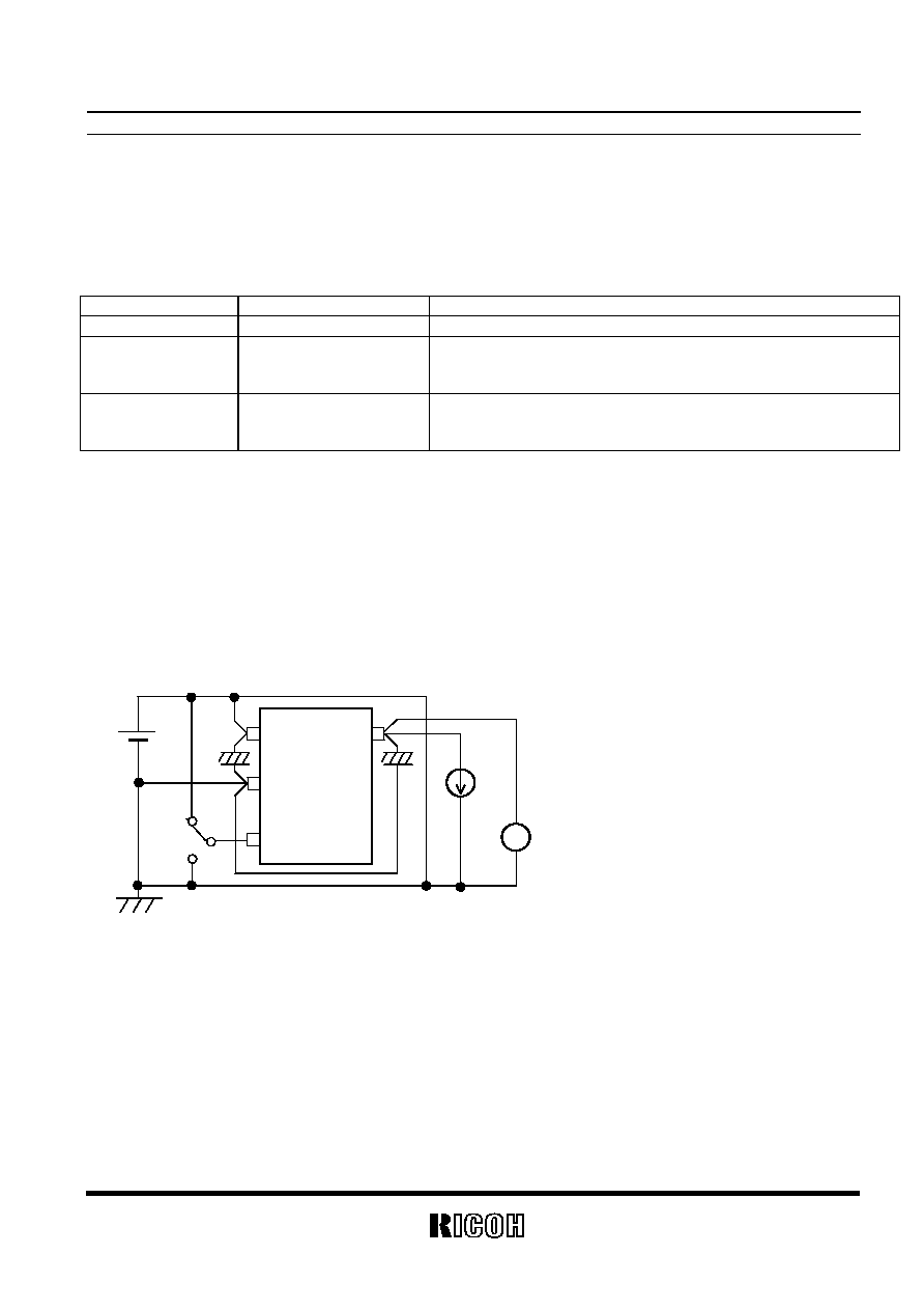
Mounting on PCB
Make V
DD
and GND lines sufficient. If their impedance is high, a current flows, the noise picked up or unstable
operation may result. Further use a 4.7µF or more value capacitor between V
DD
pin and GND pin as close as
possible.
Set an Output capacitor between V
OUT
pin and GND pin for phase compensation as close as possible.
(Refer to the example of typical application)
Example of the typical application of R1173xxxx (Fixed Output Type)
C1
C2
V
IN
V
I
OUT
VDD
OUT
CE
GND
R11 73
SERIES

R1173x
10
Technical Notes on Output Voltage Setting of Adjustable Output type (R1173x001x)
GND
R1
R
IC
V
OUT
ADJ
R2
I1
I2
1.0V
V
OUT
I
IC
The Output Voltage may be adjustable for any output voltage between its 1.0V reference and its V
DD
setting level.
An external pair of resistors is required, as shown above.
The complete equation for the output voltage is described step by step as follows;
I1=I
IC
+I2 ........................................................................................(1)
I2=1.0/R2......................................................................................(2)
Thus,
I1=I
IC
+1.0/R2 ................................................................................(3)
Therefore,
V
OUT
=1.0+R1*I1 ............................................................................(4)
Put Equation (3) into Equation (4),then
V
OUT
=1.0+R1(I
IC
+1.0/R2)
=1.0(1+R1/R2)+R1*I
IC
...........................................................(5)
In 2nd term, or R1*I
IC
will produce an error in V
OUT
.
In Equation (5),
I
IC
=1.0/R
IC
.....................................................................................(6)
R1*I
IC
=R1*1.0/R
IC
=1.0*R1/R
IC
...........................................................................(7)
For better accuracy, choosing R1 (<<R
IC
) reduces this error.

R1173x)
11
R
IC
Temperature Characteristics Example
TYPICAL CHARACTERISTICS
1) Output Voltage vs. Output Current (Topt
=
=
=
=
25∞C)
R1173X081X R1173X151X
R1173X301X
R1173X001X
0.8
1.0
1.2
1.4
1.6
1.8
2.0
-50
-25
0
25
50
75
100
Temperature Topt[
∞
C]
RI
C [
M
]
0.0
0.1
0.2
0.3
0.4
0.5
0.6
0.7
0.8
0.9
0
500
1000
1500
2000
Output Current I
OUT
[mA]
Out
put
V
o
l
t
age V
OU
T
[V]
Vdd=1.4V
Vdd=1.5V
Vdd=1.6V
Vdd=2.0V
Vdd=2.8V
0.0
0.2
0.4
0.6
0.8
1.0
1.2
1.4
1.6
0
500
1000
1500
2000
Output Current I
OUT
[mA]
Out
put
V
o
l
t
age V
OU
T
[V]
Vdd=1.8V
Vdd=2.5V
Vdd=3.5V
0.0
0.4
0.8
1.2
1.6
2.0
2.4
2.8
3.2
0
500
1000
1500
2000
Output Current I
OUT
[mA]
Out
put
V
o
l
t
age V
OU
T
[V]
Vdd=3.3V
Vdd=4.0V
Vdd=5.0V

R1173x
12
R1173X401X R1173X501X
2) Output Voltage vs. Input Voltage (Topt
=
=
=
=
25∞C)
R1173X081X R1173X151X
R1173X301X R1173X401X
0.0
0.5
1.0
1.5
2.0
2.5
3.0
3.5
4.0
4.5
0
500
1000
1500
2000
Output Current I
OUT
[mA]
Out
put
V
o
l
t
age V
OUT
[V]
Vdd=4.3V
Vdd=5.0V
Vdd=6.0V
0.0
1.0
2.0
3.0
4.0
5.0
6.0
0
500
1000
1500
2000
Output Current I
OUT
[mA]
Out
put
V
o
l
t
age V
OUT
[V]
Vdd=5.3V
Vdd=6.0V
0.0
0.2
0.4
0.6
0.8
1.0
1.2
0
1
2
3
4
5
6
Input Voltage V
IN
[V]
O
u
tput V
o
ltage V
OUT
[V]
Iout=1mA
Iout=50mA
Iout=99mA
Iout=300mA
0.0
0.2
0.4
0.6
0.8
1.0
1.2
1.4
1.6
0
1
2
3
4
5
6
Input Voltage V
IN
[V]
Out
put
V
o
l
t
age V
OUT
[V]
Iout=1mA
Iout=50mA
Iout=99mA
Iout=300mA
0.0
0.4
0.8
1.2
1.6
2.0
2.4
2.8
3.2
0
1
2
3
4
5
6
Input Voltage V
IN
[V]
Out
put
V
o
l
t
age V
OU
T
[V]
Iout=1mA
Iout=50mA
Iout=99mA
Iout=300mA
0.0
0.5
1.0
1.5
2.0
2.5
3.0
3.5
4.0
4.5
0
1
2
3
4
5
6
Input Voltage V
IN
[V]
Out
put
V
o
l
t
age V
OUT
[V]
Iout=1mA
Iout=50mA
Iout=99mA
Iout=300mA

R1173x)
13
R1173X501X
3) Dropout Voltage vs. Output Current (Topt
=
=
=
=
25∞C)
R1173X081X R1173X151X
R1173X301X R1173X401X
0.0
0.5
1.0
1.5
2.0
2.5
3.0
3.5
4.0
4.5
5.0
5.5
0
1
2
3
4
5
6
Input Voltage V
IN
[V]
Out
put
V
o
l
t
age V
OU
T
[V]
Iout=1mA
Iout=50mA
Iout=99mA
Iout=300m
A
0
10
20
30
40
50
60
70
0
1
2
3
4
5
6
Input Voltage V
IN
[V]
S
uppl
y
Current
I
SS
[
µ
A]
0
10
20
30
40
50
60
70
0
1
2
3
4
5
6
Input Voltage V
IN
[V]
S
uppl
y
Current
I
SS
[
µ
A]
0
10
20
30
40
50
60
70
0
1
2
3
4
5
6
Input Voltage V
IN
[V]
S
uppl
y
Current
I
SS
[
µ
A]
0
10
20
30
40
50
60
70
0
1
2
3
4
5
6
Input Voltage V
IN
[V]
S
uppl
y
Current
I
SS
[
µ
A]

R1173x
14
R1173X501X
4) Output Voltage vs. Temperature (I
OUT
=100mA)
R1173X081X (V
IN
=1.8V) R1173X151X
(V
IN
=2.5V)
R1173X301X (V
IN
=4.0V) R1173X501X
(V
IN
=6.0V)
0
10
20
30
40
50
60
70
0
1
2
3
4
5
6
Input Voltage V
IN
[V]
S
uppl
y
Current
I
SS
[
µ
A]
0.76
0.77
0.78
0.79
0.8
0.81
0.82
0.83
-50
-25
0
25
50
75
100
Temperature Topt[
∞
C]
Out
put
Vol
t
age V
OUT
[V
]
1.46
1.47
1.48
1.49
1.5
1.51
1.52
1.53
-50
-25
0
25
50
75
100
Temperature Topt[
∞
C]
Out
put
Vol
t
age V
OUT
[V
]
2.92
2.94
2.96
2.98
3
3.02
3.04
3.06
-50
-25
0
25
50
75
100
Temperature Topt[
∞
C]
O
u
tput V
o
ltage V
OU
T
[V
]
4.88
4.9
4.92
4.94
4.96
4.98
5
5.02
-50
-25
0
25
50
75
100
Temperature Topt[
∞
C]
O
u
tput V
o
ltage V
OUT
[V
]

R1173x)
15
5) Supply Current vs. Temperature
R1173X081X (V
IN
=1.8V) R1173X151X
(V
IN
=2.5V)
R1173X301X (V
IN
=4.0V) R1173X501X
(V
IN
=6.0V)
6) Dropout Voltage vs. Output Current
R1173X081X R1173X091X
0
10
20
30
40
50
60
70
80
-50
-25
0
25
50
75
100
Temperature Topt[
∞
C]
S
upply
C
u
r
r
ent I
SS
[
µ
A]
0
10
20
30
40
50
60
70
80
-50
-25
0
25
50
75
100
Temperature Topt[∞C]
S
upply
C
u
r
r
ent I
SS
[
µ
A]
0
10
20
30
40
50
60
70
80
-50
-25
0
25
50
75
100
Temperature Topt[
∞
C]
S
upply C
u
rrent I
SS
[
µ
A]
0
10
20
30
40
50
60
70
80
-50
-25
0
25
50
75
100
Temperature Topt[
∞
C]
S
upply
C
u
r
r
ent I
SS
[
µ
A]
0
100
200
300
400
500
600
700
800
0
200
400
600
800
1000
Output Current I
OUT
[mA]
Dropout
V
o
l
t
age V
DI
F
[mV]
85∞C
25∞C
-40∞C
0
100
200
300
400
500
600
700
0
200
400
600
800
1000
Output Current I
OUT
[mA]
D
r
opout V
o
ltage V
DIF
[m
V]
85∞C
25∞C
-40∞C

R1173x
16
R1173X101X R1173X151X
R1173X301X R1173X501X
7) Dropout Voltage vs. Set Output Voltage 8) 0.8V Output type, Operating Input Voltage Range
R1173XXX1X R1173X081X
0
100
200
300
400
500
600
700
800
0
1
2
3
4
5
Set Output Voltage V
REG
[V]
Dropout
V
o
l
t
age V
DI
F
[mV]
100mA
200mA
400mA
600mA
800mA
1000mA
0.8
1
1.2
1.4
1.6
1.8
0
200
400
600
800
1000
Output Current I
OUT
[mA]
Input V
o
ltage V
IN
[V]
Operating Input Voltage Range
0
50
100
150
200
250
0
200
400
600
800
1000
Output Current I
OUT
[mA]
Dropout
V
o
l
t
age V
DI
F
[mV]
85∞C
25∞C
-40∞C
0
20
40
60
80
100
120
140
160
180
200
0
200
400
600
800
1000
Output Current I
OUT
[mA]
D
r
opout V
o
ltage V
DI
F
[m
V]
85
25
-40
0
50
100
150
200
250
300
350
400
0
200
400
600
800
1000
Output Current I
OUT
[mA]
D
r
opout V
o
ltage V
DIF
[m
V
]
85∞C
25∞C
-40∞C
0
100
200
300
400
500
600
0
200
400
600
800
1000
Output Current I
OUT
[mA]
D
r
opout V
o
ltage V
DI
F
[m
V]
85∞C
25∞C
-40∞C

R1173x)
17
9) Ripple Rejection vs. Input Bias
R1173X301X (V
IN
=4.0V
DC
+0.2Vp-p, I
OUT
=1mA) R1173X301X
(V
IN
=4.0V
DC
+0.5Vp-p, I
OUT
=1mA)
R1173X301X (V
IN
=4.0V
DC
+0.2Vp-p, I
OUT
=10mA) R1173X301X
(V
IN
=4.0V
DC
+0.5Vp-p, I
OUT
=10mA)
R1173X301X (V
IN
=4.0V
DC
+0.2Vp-p, I
OUT
=100mA) R1173X301X
(V
IN
=4.0V
DC
+0.5Vp-p, I
OUT
=100mA)
0
10
20
30
40
50
60
70
80
90
3.000
3.100
3.200
3.300
3.400
3.500
Input Voltage V
IN
[V]
Ri
ppl
e Rej
e
c
t
i
o
n
RR[
d
B
]
200Hz
1kHz
10kHz
100kHz
0
10
20
30
40
50
60
70
80
90
3.000
3.100
3.200
3.300
3.400
3.500
Input Voltage V
IN
[V]
Ri
ppl
e Rej
e
c
t
i
o
n
RR[
d
B
]
200Hz
1kHz
10kHz
100kHz
0
10
20
30
40
50
60
70
80
90
3.000
3.100
3.200
3.300
3.400
3.500
Input Voltage V
IN
[V]
Ri
p
p
l
e
Re
j
e
c
t
i
o
n
RR[
d
B
]
200Hz
1kHz
10kHz
100kHz
0
10
20
30
40
50
60
70
80
90
3.000
3.100
3.200
3.300
3.400
3.500
Input Voltage V
IN
[V]
Ri
p
p
l
e
Re
j
e
cti
o
n
RR[d
B
]
200Hz
1kHz
10kHz
100kHz
0
10
20
30
40
50
60
70
80
90
3.000
3.100
3.200
3.300
3.400
3.500
Input Voltage V
IN
[V]
Ri
p
p
l
e
Re
j
e
c
t
i
o
n
RR[d
B
]
200Hz
1kHz
10kHz
100kHz
0
10
20
30
40
50
60
70
80
90
3.000
3.100
3.200
3.300
3.400
3.500
Input Voltage V
IN
[V]
Ri
p
p
l
e
Re
j
e
cti
o
n
RR[d
B
]
200Hz
1kHz
10kHz
100kHz

R1173x
18
10) Ripple Rejection vs. Frequency
R1173X081X (VIN
=1.8V
DC
+0.5Vp-p, C
OUT
=Tantalum 4.7
µ
µ
µ
µ
F)
R1173X101X (VIN
=2.0V
DC
+0.5Vp-p, C
OUT
=Ceramic 4.7
µ
µ
µ
µ
F)
R1173X301X (VIN
=4.0V
DC
+0.5Vp-p, C
OUT
=Ceramic 4.7
µ
µ
µ
µ
F)
R1173X401X (VIN
=5.0V
DC
+0.5Vp-p, C
OUT
=Ceramic 4.7
µ
µ
µ
µ
F)
R1173X451X (VIN
=5.5V
DC
+0.5Vp-p, C
OUT
=Ceramic 4.7
µ
µ
µ
µ
F)
R1173X501X (VIN
=6.0V
DC
+0.5Vp-p, C
OUT
=Ceramic 4.7
µ
µ
µ
µ
F)
0
10
20
30
40
50
60
70
80
0.1
1
10
100
Frequency f[kHz]
Ri
ppl
e Rej
e
ct
i
o
n
RR[
dB]
IOUT=1mA
IOUT=30mA
IOUT=100mA
0
10
20
30
40
50
60
70
80
90
0.1
1
10
100
Frequency f[kHz]
Ri
p
p
l
e
Re
j
e
c
t
i
o
n
RR[d
B
]
IOUT=1mA
IOUT=30mA
IOUT=100mA
0
10
20
30
40
50
60
70
80
90
0.1
1
10
100
Frequency f[kHz]
Ri
p
p
l
e
Re
j
e
c
t
i
o
n
RR[
d
B
]
IOUT=1mA
IOUT=30mA
IOUT=100mA
0
10
20
30
40
50
60
70
80
90
0.1
1
10
100
Frequency f[kHz]
Ri
ppl
e Rej
e
ct
i
o
n
RR[
dB]
IOUT=1mA
IOUT=30mA
IOUT=100mA
0
10
20
30
40
50
60
70
80
0.1
1
10
100
Frequency f[kHz]
Ri
ppl
e Rej
e
c
t
i
o
n
RR[
dB
]
IOUT=1mA
IOUT=30mA
IOUT=100mA
0
10
20
30
40
50
60
70
80
0.1
1
10
100
Frequency f[kHz]
Ri
p
p
l
e
Re
j
e
c
t
i
o
n
RR[
d
B
]
IOUT=1mA
IOUT=30mA
IOUT=100mA

R1173x)
19
11) Line Transient Response (Tr = Tf =5
µ
µ
µ
µ
s, I
OUT
=100mA)
R1173X081X (C
OUT
=Tantalum 4.7
µ
µ
µ
µ
F)
R1173X101X (C
OUT
=Ceramic 4.7
µ
µ
µ
µ
F)
R1173X301X (C
OUT
=Ceramic 4.7
µ
µ
µ
µ
F)
R1173X501X (C
OUT
=Ceramic 4.7
µ
µ
µ
µ
F)
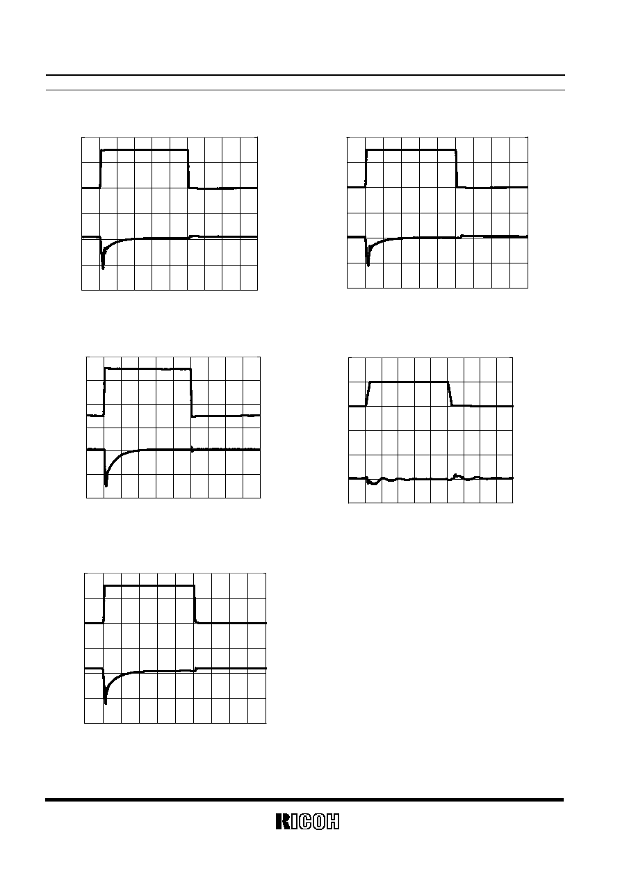
12) Load Transient Response (Tr=Tf=500ns)
R1173X081X (V
IN
=1.8V, C
IN
=C
OUT
=Tantalum 4.7
µ
µ
µ
µ
F)
R1173X081X (V
IN
=1.8V, C
IN
=C
OUT
=Tantalum 4.7
µ
µ
µ
µ
F)
0.76
0.78
0.8
0.82
0.84
0.86
0.88
0.9
0
10 20 30 40 50 60 70 80 90 100
Time T[µs]
Out
put
V
o
l
t
age V
OU
T
[V]
-3
-2
-1
0
1
2
3
4
I
nput
V
o
l
t
age V
IN
[V]
0.96
0.98
1
1.02
1.04
1.06
1.08
1.1
0
10 20 30 40 50 60 70 80 90 100
Time T[µs]
O
u
tput V
o
ltage V
OUT
[V]
-3
-2
-1
0
1
2
3
4
Input V
o
ltage V
IN
[V]
Input Voltage
Output Voltage
Input Voltage
Output Voltage
4.94
4.97
5
5.03
5.06
5.09
5.12
5.15
0
10 20 30 40 50 60 70 80 90 100
Time T[µs]
Out
put
V
o
l
t
age V
OU
T
[V]
0
1
2
3
4
5
6
7
I
nput
V
o
l
t
age V
IN
[V]
2.94
2.97
3
3.03
3.06
3.09
3.12
3.15
0
10 20 30 40 50 60 70 80 90 100
Time T[µs]
Out
put
V
o
l
t
age V
OU
T
[V]
-1
0
1
2
3
4
5
6
I
nput
V
o
l
t
age V
IN
[V]
Input Voltage
Output Voltage
Input Voltage
Output Voltage
0.68
0.74
0.8
0.86
0.92
0.98
1.04
0
10 20 30 40 50 60 70 80 90 100
Time T[µs]
O
u
tput V
o
ltage V
OUT
[V
]
-600
-400
-200
0
200
400
600
O
u
tput C
u
rrent I
OUT
[m
A
]
Output Voltage
Output Current
0.76
0.8
0.84
0.88
0.92
0.96
1
0
2
4
6
8 10 12 14 16 18 20
Time T[µs]
O
u
tput V
o
ltage V
OUT
[V
]
-150
-100
-50
0
50
100
150
O
u
tput C
u
rrent I
OUT
[m
A
]
Output Current
Output Voltage

R1173x
20
R1173X081X (V
IN
=1.8V, C
IN
=C
OUT
=Tantalum 4.7
µ
F)
R1173X081X (VIN=1.8V,CIN=Tantalum4.7
µ
F, COUT=Tantalum10
µ
F)
R1173X101X (V
IN
=2.0V, C
IN
=C
OUT
=Ceramic 4.7
µ
F)
R1173X101X (VIN=2.0V, CIN=Ceramic 4.7
µ
F, COUT
= Ceramic
10
µ
F)
R1173X101X (V
IN
=2.0V, C
IN
=C
OUT
=Ceramic 4.7
µ
F)
R1173X101X (VIN=2.0V, CIN=Ceramic 4.7
µ
F, COUT
= Ceramic
10
µ
F)
0.76
0.8
0.84
0.88
0.92
0.96
1
0
10 20 30 40 50 60 70 80 90 100
Time T[µs]
Output Vol
t
age V
OU
T
[V]
-80
-60
-40
-20
0
20
40
Output Cur
r
ent I
OU
T
[mA]
Output Voltage
Output Current
0.76
0.8
0.84
0.88
0.92
0.96
1
0
10 20 30 40 50 60 70 80 90 100
Time T[µs]
O
u
tput V
o
ltage V
OUT
[V]
-80
-60
-40
-20
0
20
40
O
u
tput C
u
rrent I
OUT
[mA]
Output
Current
Output
Voltage
0.8
0.9
1
1.1
1.2
1.3
1.4
0
10 20 30 40 50 60 70 80 90 100
Time T[µs]
Out
put
V
o
l
t
age V
OUT
[V]
-600
-400
-200
0
200
400
600
Out
put
Current
I
OUT
[mA]
Output
Current
Output
Voltage
0.8
0.9
1
1.1
1.2
1.3
1.4
0
10 20 30 40 50 60 70 80 90 100
Time T[µs]
Out
put
V
o
l
t
age V
OUT
[V]
-600
-400
-200
0
200
400
600
Out
put
Current
I
OUT
[mA]
Output
Current
Output
Voltage
0.96
1
1.04
1.08
1.12
1.16
1.2
0
4
8 12 16 20 24 28 32 36 40
Time T[µs]
Out
put
Vol
t
age V
OUT
[V
]
-150
-100
-50
0
50
100
150
Out
put
Cur
r
ent
I
OUT
[m
A
]
Output
Current
Output
Voltage
0.96
1
1.04
1.08
1.12
1.16
1.2
0
2
4
6
8
10 12 14 16 18 20
Time T[µs]
output V
o
ltage V
OUT
[V
]
-150
-100
-50
0
50
100
150
O
u
tput C
u
rrent I
OUT
[m
A
]
Output
Current
Output
Voltage

R1173x)
21
R1173X101X (V
IN
=2.0V, C
IN
=C
OUT
=Ceramic 4.7
µ
F)
R1173X101X (VIN=2.0V, CIN=Ceramic 4.7
µ
F, COUT
= Ceramic
10
µ
F)
R1173X301X (V
IN
=4.0V, C
IN
=C
OUT
=Ceramic 4.7
µ
F) R1173X301X
(V
IN
=4.0V, C
IN
=Ceramic 4.7
µ
F, C
OUT
=
Ceramic 10
µ
F)
R1173X301X (V
IN
=4.0V, C
IN
=C
OUT
=Ceramic 4.7
µ
F) R1173X301X
(V
IN
=4.0V, C
IN
=Ceramic 4.7
µ
F, C
OUT
=
Ceramic 10
µ
F)
0.9
0.95
1
1.05
1.1
1.15
1.2
0
10 20 30 40 50 60 70 80 90 100
Time T[µs]
O
u
tput V
o
ltage V
OU
T
[V
]
-80
-60
-40
-20
0
20
40
O
u
tput C
u
rrent I
OU
T
[m
A
]
Output
Current
Output
Voltage
0.9
0.95
1
1.05
1.1
1.15
1.2
0
10 20 30 40 50 60 70 80 90 100
Time T[µs]
O
u
tput V
o
ltage V
OUT
[V
]
-80
-60
-40
-20
0
20
40
O
u
tput C
u
rrent I
OUT
[m
A
]
Output
Current
Output
Voltage
2.6
2.8
3
3.2
3.4
3.6
3.8
0
40 80 120 160 200 240 280 320 360 400
Time T[µs]
Output V
o
ltage V
OUT
[V]
-600
-400
-200
0
200
400
600
Output C
u
rrent I
OUT
[mA]
Output
Current
Output
Voltage
2.6
2.8
3
3.2
3.4
3.6
3.8
0
40
80 120 160 200 240 280 320 360 400
Time T[µs]
Out
put
V
o
l
t
age V
OU
T
[V]
-600
-400
-200
0
200
400
600
Out
put
Current
I
OU
T
[mA]
Output
Current
Output
Voltage
2.96
3
3.04
3.08
3.12
3.16
3.2
0
4
8 12 16 20 24 28 32 36 40
Time T[µs]
O
u
tput V
o
ltage V
OUT
[V]
-150
-100
-50
0
50
100
150
O
u
tput C
u
rrent I
OUT
[mA]
Output
Current
Output
Voltage
2.96
3
3.04
3.08
3.12
3.16
3.2
0
2
4
6
8
10 12 14 16 18 20
Time T[µs]
O
u
tput V
o
ltage V
OUT
[V]
-150
-100
-50
0
50
100
150
O
u
tput C
u
rrent I
OUT
[m
A]
Output
Current
Output
Voltage
R1173x
22
R1173X301X (V
IN
=4.0V, C
IN
=C
OUT
=Ceramic 4.7
µ
F) R1173X301X
(V
IN
=4.0V, C
IN
=Ceramic 4.7
µ
F, C
OUT
=
Ceramic 10
µ
F)
R1173X501X (V
IN
=6.0V, C
IN
=C
OUT
=Ceramic 4.7
µ
F) R1173X501X
(V
IN
=6.0V, C
IN
=C
OUT
= Ceramic 4.7
µ
F)
R1173X501X (V
IN
=6.0V, C
IN
=C
OUT
=Ceramic 4.7
µ
F)
2.9
2.95
3
3.05
3.1
3.15
3.2
0
40 80 120 160 200 240 280 320 360 400
Time T[µs]
Out
put
Vol
t
age V
OUT
[V
]
-80
-60
-40
-20
0
20
40
Out
put
Cur
r
ent
I
OUT
[m
A
]
Output
Current
Output
Voltage
2.9
2.95
3
3.05
3.1
3.15
3.2
0
40 80 120 160 200 240 280 320 360 400
Time T[µs]
Out
put
Vol
t
age V
OUT
[V
]
-80
-60
-40
-20
0
20
40
Out
put
Cur
r
ent
I
OUT
[m
A
]
Output
Current
Output
Voltage
4.5
4.75
5
5.25
5.5
5.75
6
0
40 80 120 160 200 240 280 320 360 400
Time T[µs]
O
u
tput V
o
ltage V
OUT
[V]
-600
-400
-200
0
200
400
600
O
u
tput C
u
rrent I
OUT
[m
A]
Output
Current
Output
Voltage
4.96
5
5.04
5.08
5.12
5.16
5.2
0
2
4
6
8 10 12 14 16 18 20
Time T[µs]
O
u
tput V
o
ltage V
OUT
[V
]
-150
-100
-50
0
50
100
150
O
u
tput C
u
rrent I
OUT
[m
A
]
Output
Voltage
Output
Current
4.9
4.95
5
5.05
5.1
5.15
5.2
0
40 80 120 160 200 240 280 320 360 400
Time T[µs]
O
u
tput V
o
ltage V
OU
T
[V]
-80
-60
-40
-20
0
20
40
O
u
tput C
u
rrent I
OU
T
[m
A]
Output
Current
Output
Voltage

R1173x)
23
13) Turn-on speed with CE pin control
R1173X081X (V
IN
=1.8V, C
IN
=C
OUT
=Tantalum 4.7
µ
F)
R1173X501X (V
IN
=6.0V, C
IN
=C
OUT
=Ceramic 4.7
µ
F)
14) Turn-off speed with CE pin control
R1173X081D (V
IN
=1.8V, C
IN
=C
OUT
=Tantalum 4.7
µ
F)
R1173X501D (V
IN
=6.0V, C
IN
=C
OUT
=Ceramic 4.7
µ
F)
-0.2
0
0.2
0.4
0.6
0.8
1
1.2
1.4
1.6
1.8
-20 0
20 40 60 80 100 120 140 160 180
Time T[µs]
Out
put
V
o
l
t
age V
OUT
[V]
-2.0
-1.6
-1.2
-0.8
-0.4
0.0
0.4
0.8
1.2
1.6
2.0
CE
I
nput
V
o
l
t
age V
CE
[V]
IOUT=0mA
IOUT=100mA
IOUT=300mA
VCE
-2
0
2
4
6
8
10
-40
60
160
260
360
Time T[µs]
O
u
tput V
o
ltage V
OU
T
[V
]
-4
-2
0
2
4
6
8
C
E
Input V
o
ltage V
CE
[V
]
IOUT=0mA
IOUT=100mA
IOUT=300mA
Vin (V)
-0.2
0
0.2
0.4
0.6
0.8
1
1.2
1.4
1.6
1.8
2
-0.4
0.6
1.6
2.6
3.6
Time T[ms]
Out
put
Vol
t
age V
OUT
[V
]
-2.4
-2
-1.6
-1.2
-0.8
-0.4
0
0.4
0.8
1.2
1.6
2
CE I
nput
Vol
t
age V
CE
[V
]
IOUT=0mA
IOUT=100mA
IOUT=300mA
Vin (V)
-2
0
2
4
6
8
10
12
14
-0.2
0.2
0.6
1
1.4
1.8
Time T[ms]
output V
o
ltage V
OU
T
[V
]
-8
-6
-4
-2
0
2
4
6
8
C
E
Input V
o
ltage V
CE
[V
]
IOUT=0mA
IOUT=100mA
IOUT=300mA
Vin (V)

R1173x
24
15) Inrush Current (I
OUT
=100mA, C
IN
=none)
R1173X081X (V
IN
=2.0V, C
OUT
=Tantalum 4.7
µ
F)
R1173X081X (V
IN
=2.0V, C
OUT
=Tantalum 10
µ
F)
R1173X301X (V
IN
=4.0V, C
OUT
=Ceramic 4.7
µ
F)
R1173X301X (V
IN
=4.0V, C
OUT
=Ceramic 10
µ
F)
-4
-3.2
-2.4
-1.6
-0.8
0
0.8
1.6
2.4
-40
0
40
80
120
160
Time t (us)
CE
V
o
l
t
age V
c
e,
Out
put
V
o
l
t
age
V
out
(V
)
-200
0
200
400
600
800
1000
1200
1400
I
n
rus
h
Current
V
dd (m
A
)
Output
Voltage
CE Input Voltage
Inrush
Current
-4
-3.2
-2.4
-1.6
-0.8
0
0.8
1.6
2.4
-40
0
40
80
120
160
Time t (us)
CE
V
o
l
t
age V
c
e,
Out
put
V
o
l
t
age
V
out
(V
)
-200
0
200
400
600
800
1000
1200
1400
I
n
rus
h
Current
I
v
dd (m
A
)
CE Input Voltage
Output
Voltage
Inrush
Current
-5
-4
-3
-2
-1
0
1
2
3
4
5
-40
0
40
80
120
160
Time t (us)
CE
V
o
l
t
age V
c
e,
Out
put
V
o
l
t
age
V
out
(V
)
-200
0
200
400
600
800
1000
1200
1400
1600
1800
I
n
rus
h
Current
I
v
dd (m
A
)
CE Input Voltage
Output
Voltage
Inrush
Current
-5
-4
-3
-2
-1
0
1
2
3
4
5
-40
0
40
80
120
160
Time t (us)
CE
V
o
l
t
age V
c
e,
Out
put
V
o
l
t
age
V
out
(V
)
-200
0
200
400
600
800
1000
1200
1400
1600
1800
In
r
u
sh
C
u
r
r
e
n
t
Ivd
d
(
m
A)
CE Input Voltage
Output
Voltage
Inrush
Current
R1173x)
25
R1173X501X (V
IN
=6.0V, C
OUT
=Ceramic 4.7
µ
F)
R1173X501X (V
IN
=6.0V, C
OUT
=Ceramic 10
µ
F)
16)
Stable Area: ESR limit vs. Load current (C
OUT
:0.8V to 3.3V Output type: 4.7
µ
F (Kyocera CM105X5R475M06AB)
5.0V Output type: 4.7
µ
F(Kyocera CT21X5R475K06AB)
As an output capacitor for this IC, Ceramic capacitor is recommendable. However, other low ESR type capacitor can be
used with this IC.
For your reference, noise level is tested, and if the noise level is 40
µ
V or less than 40
µ
V, the ESR values are plotted as
stable area. Upper limit is described in the next five graphs, or ESR vs. Output Current. (Hatched area is the stable area.)
R1173X081X (VIN
=1.4V to 6.0V, C
IN
= C
OUT
= Ceramic
4.7
µ
F)
R1173X081X (V
IN
=1.4V to 6.0V, C
IN
= Ceramic 4.7
µ
F, C
OUT
=
Ceramic 10
µ
F)
-10
-8
-6
-4
-2
0
2
4
6
8
-40
0
40
80
120
160
Time t (us)
CE
V
o
l
t
age V
c
e,
Out
put
V
o
l
t
age
V
out
(V
)
-200
0
200
400
600
800
1000
1200
1400
1600
I
n
rus
h
Current
I
v
dd (m
A
)
CE Input Voltage
Output
Voltage
Inrush
Current
-10
-8
-6
-4
-2
0
2
4
6
8
-40
0
40
80
120
160
Time t (us)
CE
V
o
l
t
age V
c
e,
Out
put
V
o
l
t
age
V
out
(V
)
-200
0
200
400
600
800
1000
1200
1400
1600
I
n
rus
h
Current
I
v
dd (m
A
)
CE Input Voltage
Output
Voltage
Inrush
Current
0.01
0.1
1
10
100
0
200
400
600
800
1000
Load Current I
OUT
[mA]
ESR
[
]
Topt=85
∞
C
Topt=-40
∞
C
0.01
0.1
1
10
100
0
200
400
600
800
1000
Load Current I
OUT
[mA]
ESR
[
]
Topt=85
∞
C
Topt=-40
∞
C

R1173x
26
R1173X101X (VIN=1.4V to 6.0V, CIN = COUT = Ceramic 4.7
µ
F)
R1173X301X (VIN=3.1V to 6.0V, CIN = COUT = Ceramic 4.7
µ
F)
R1173X501X (VIN=5.3V to 6.0V, CIN = COUT = Ceramic 4.7
µ
F)
0.01
0.1
1
10
100
0
200
400
600
800
1000
Load Current I
OUT
[mA]
ESR
[
]
Topt=-40
∞
C
Topt=85
∞
C
0.01
0.1
1
10
100
0
200
400
600
800
1000
Load Current I
OUT
[mA]
ESR
[
]
Topt=85
∞
C
Topt=-40
∞
C
0.01
0.1
1
10
100
0
200
400
600
800
1000
Load Current I
OUT
[mA]
ESR
[
]
Topt=85
∞
C
Topt=-40
∞
C