
Step-down DC/DC Converter with Voltage Detector
R1221N Series
`
99.12.8
1
1
1
122223
3
3
345
45
45
45
12345
Rev. 1.11 - 1 -
n
n
n
n
OUTLINE
The R1221N Series are PWM step-down DC/DC Converter controllers embedded with a voltage detector, with
low supply current by CMOS process.
Each
step-down DC/DC converter in these ICs consists of an oscillator, a PWM control circuit, a reference
voltage unit, an error amplifier, a soft-start circuit, a protection circuit, a PWM/VFM alternative circuit, a chip
enable circuit, and resistors for voltage detection. A low ripple, high efficiency step-down DC/DC converter can be
composed of this IC with only four external components, or a power-transistor, an inductor, a diode and a
capacitor.
The output voltage of DC/DC converter can be supervised by the built-in voltage detector.
With a PWM/VFM alternative circuit, when the load current is small, the operation turns into the VFM oscillator
from PWM oscillator automatically, therefore the efficiency at small load current is improved.
And the PWM/VFM alternative circuit is an option, in terms of C version and D version, the circuit is not included.
If the term of maximum duty cycle keeps on a certain time, the embedded protection circuit works. There are two
types of protection function. One is latch-type protection circuit, and it works to latch an external Power MOS with
keeping it disable. To release the condition of protection, after disable this IC with a chip enable circuit, enable it
again, or restart this IC with power-on. The other is Reset-type protection circuit, and it works to restart the
operation with soft-start and repeat this operation until maximum duty cycle condition is released. Either of these
protection circuits can be designated by users' request.
n
n
n
n
FEATURES
l
Wide Range of Input Voltage
∑
∑
∑
∑
∑
∑
∑
∑
∑
∑
∑
∑
∑
2.3V to 13.2V
l
Built-in Soft-start Function and two choices of Protection Function(Latch-type or Reset-type)
l
Two choices of Oscillator Frequency
∑
∑
∑
∑
∑
∑
∑
∑
∑
∑
300kHz, 500kHz
l
High Efficiency
∑
∑
∑
∑
∑
∑
∑
∑
∑
∑
∑
∑
∑
∑
∑
∑
∑
∑
∑
∑
∑
∑
TYP. 90%
l
Standby Current
∑
∑
∑
∑
∑
∑
∑
∑
∑
∑
∑
∑
∑
∑
∑
∑
∑
∑
∑
∑
∑
TYP. 0µA
l
Setting Output Voltage
∑
∑
∑
∑
∑
∑
∑
∑
∑
∑
∑
∑
∑
∑
∑
∑
∑
Stepwise setting with a step of 0.1V in the range of
1.5V to 5.0V
l
High Accuracy Output Voltage
∑
∑
∑
∑
∑
∑
∑
∑
∑
∑
∑
∑
∑
∑
±2.0%
l
Setting Detector Threshold Voltage
∑
∑
∑
∑
∑
∑
∑
∑
∑
∑
∑
Stepwise setting with a step of 0.1V in the range of
1.2V to 4.5V
l
High Accuracy Detector Threshold Voltage
∑
∑
∑
∑
∑
∑
∑
±2.0%
l
Low Temperature-Drift Coefficient of Output Voltage
∑
TYP. ±100ppm/
∞
C
n
n
n
n
APPLICATIONS
l
Power source for hand-held communication equipment, cameras, video instruments such as VCRs,
camcorders.
l
Power source for battery-powered equipment.
l
Power source for household electrical appliances.
12345
Rev. 1.11 - 2 -
n
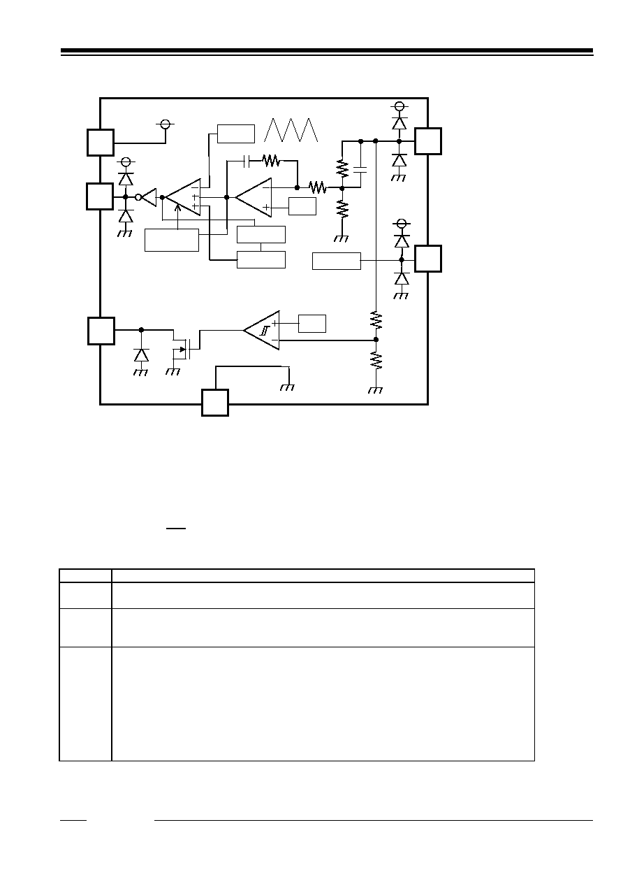
BLOCK DIAGRAM
OSC
V
IN
EXT
GND
V
OUT
Vref
Vref
CE
Chip Enable
Soft Start
Protection
PWM/VFM
CONTROL
VD
OUT
n
SELECTION GUIDE
In the R1221N Series, the output voltage, the detector threshold, the oscillator frequency, the optional
function, and the taping type for the ICs can be selected at the user's request.
The selection can be made by designating the part number as shown below;
R1221NXXXX-TR
-
-
-
a
b c
Code
Contents
a
Setting Output Voltage(V
OUT
):
Stepwise setting with a step of 0.1V in the range of 1.5V to 5.0V is possible.
b
Setting Detector Threshold(-V
DET
)
Stepwise setting with a step of 0.1V in the range of 1.2V to 4.5V is possible.
A:3.0V
c
Designation of Oscillator Frequency and Optional Function
A:300kHz, with a PWM/VFM alternative circuit, Latch-type protection
B:500kHz, with a PWM/VFM alternative circuit, Latch-type protection
C:300kHz, without a PWM/VFM alternative circuit, Latch-type protection
D:500kHz, without a PWM/VFM alternative circuit, Latch-type protection
E:300kHz, with a PWM/VFM alternative circuit, Reset-type protection
F:500kHz, with a PWM/VFM alternative circuit, Reset-type protection
G:300kHz, without a PWM/VFM alternative circuit, Reset-type protection
H:500kHz, without a PWM/VFM alternative circuit, Reset-type protection
12345
Rev. 1.11 - 3 -
n
n
n
n
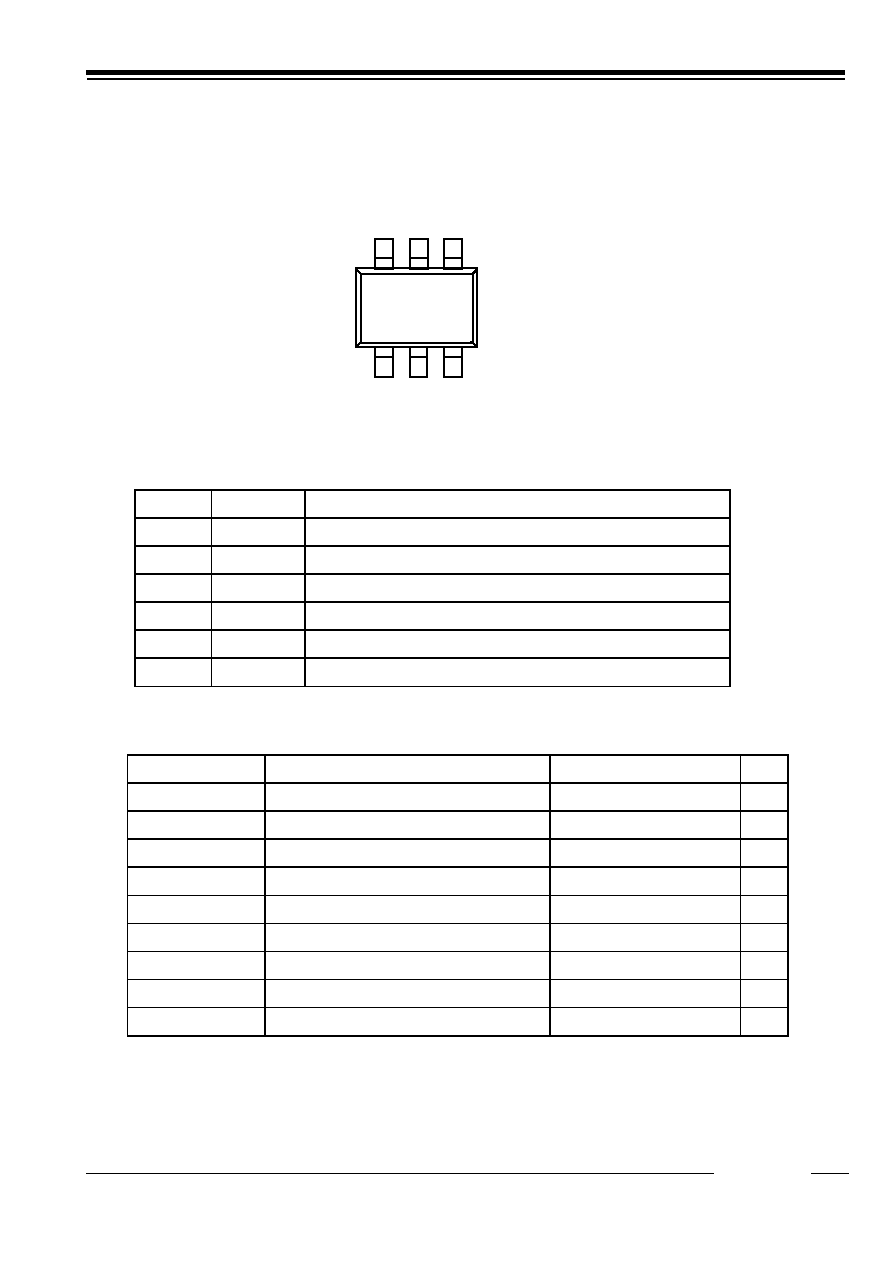
PIN CONFIGURATION
l
SOT-23-6W
1
2
3
4
6
V
OUT
GND CE
EXT VD
OUT
V
IN
(mark side)
5
n
n
n
n
PIN DESCRIPTION
Pin No.
Symbol
Description
1
EXT
External Transistor Drive Pin (Output Type ; CMOS)
2
VD
OUT
Voltage Detector Output Pin (Output Type ; Nch Open Drain )
3
V
IN
Power Supply Pin
4
CE
Chip Enable Pin
5
GND
Ground Pin
6
V
OUT
Pin for Monitoring Output Voltage
n
n
n
n
ABSOLUTE MAXIMUM RATING
Symbol
Item
Rating
Unit
V
IN
V
IN
Supply Voltage
15
V
V
EXT
EXT Pin Output Voltage
-0.3
~
V
IN
+0.3
V
V
CE
CE Pin Input Voltage
-0.3
~
V
IN
+0.3
V
VD
OUT
VD
OUT
Pin Output Voltage
-0.3
~
15
V
V
OUT
V
OUT
Pin Input Voltage
-0.3
~
V
IN
+0.3
V
I
EXT
EXT Pin Inductor Drive Output Current
±
25
mA
P
D
Power Dissipation
250
mW
Topt
Operating Temperature Range
-40
~
+85
∞
C
Tstg
Storage Temperature Range
-55
~
+125
∞
C

12345
Rev. 1.11 - 4 -
n
n
n
n
ELECTRICAL CHARACTERISTICS
l
R1221N***A(C,E,G) Output Voltage : Vo, Detector Threshold : V
D
(Topt=25
∞
C)
Symbol
Item
Conditions
MIN. TYP. MAX.
Note*
Unit
V
IN
Operating Input Voltage
2.3
13.2
V
V
OUT
Step-down Output Voltage
V
IN
=V
CE
=Vo+1.2V, I
OUT
=-10mA
Vo
¥
0.98
Vo
Vo
¥
1.02
A
V
D
V
OUT
/
D
T
Step-down Output Voltage
Temperature Coefficient
-40
∞
C
£
Topt
£
85
∞
C
±
100
ppm/
∞
C
fosc
Oscillator Frequency
V
IN
=V
CE
=Vo+1.2V, I
OUT
=-100mA
240
300
360
A
kHz
D
f
OSC
/
D
T
Frequency Temperature
Coefficient
-40
∞
C
£
Topt
£
85
∞
C
±
0.3
%/
∞
C
I
DD1
Supply Current1
V
IN
=13.2V,V
CE
=13.2V,V
OUT
=13.2V
100
160
B
m
A
I
stb
Standby Current
V
IN
=13.2V,V
CE
=0V,V
OUT
=0V
0
0.5
C
m
A
I
EXTH
EXT "H" Output Current
V
IN
=8V,V
EXT
=7.9V,V
OUT
=8V,V
CE
=8V
-10
-6
D
mA
I
EXTL
EXT "L" Output Current
V
IN
=8V,V
EXT
=0.1V,V
OUT
=0V,V
CE
=0V
10
20
D
mA
I
CEH
CE "H" Input Current
V
IN
=13.2V,V
CE
=13.2V,V
OUT
=13.2V
0
0.5
E
m
A
I
CEL
CE "L" Input Current
V
IN
=13.2V,V
CE
=0V,V
OUT
=13.2V
-0.5
0
E
m
A
V
CEH
CE "H" Input Voltage
V
IN
=8V,V
CE
=0V
Æ
1.5V
0.8
1.2
F
V
V
CEL
CE "L" Input Voltage
V
IN
=8V,V
CE
=1.5V
Æ
0V
0.3
0.8
F
V
Maxdty Oscillator Maximum Duty Cycle
100
%
VFMdty VFM Duty Cycle
Applied to B and F versions only
25
%
T
start
Delay Time by Soft-Start
function
V
IN
=Vo+1.2V,V
CE
=0V
Æ
Vo+1.2V
At 80% of rising
5
10
16
F
ms
T
prot
Delay Time for protection circuit V
IN
=Vo+1.2V,V
CE
=Vo+1.2V
Æ
0V
1
3
5
G
ms
I
VDLK
VD
OUT
Output Leakage Current V
IN
=V
OUT
=V
CE
=V
DOUT
=8V
0
0.5
I
m
A
I
VDL
VD
OUT
"L" Output Current
V
IN
=V
OUT
=2.3V, V
CE
=0V, V
DOUT
=0.1V
0.5
1
I
mA
-V
DET
Detector Threshold
V
IN
=6V, V
CE
=6V, V
OUT
=V
D
¥
1.2V
Æ
0V
V
D
¥
0.98
V
D
V
D
¥
1.02
J
V
tV
DET
Output Delay Time for Released
Voltage
V
IN
=6V, V
CE
=6V, V
OUT
=0V
Æ
V
D
¥
1.2V
At 80% of rising
2
5
10
J
ms
V
HYS
Detector Threshold Hysteresis
V
IN
=6V, V
CE
=6V, V
OUT
=0V
Æ
V
D
¥
1.2V
V
D
¥
0.01
V
D
¥
0.03
V
D
¥
0.05
J
mV
D
-
V
DET
/
D
T
Detector Threshold
Temperature Coefficient
-40
∞
C
£
Topt
£
85
∞
C
±
100
ppm/
∞
C
Note: Refer to Test Circuits

12345
Rev. 1.11 - 5 -
l
R1221N***B(D,F,H) Output Voltage : Vo, Detector Threshold : V
D
(Topt=25
∞
C)
Symbol
Item
Conditions
MIN. TYP. MAX.
Note*
Unit
V
IN
Operating Input Voltage
2.3
13.2
V
V
OUT
Step-down Output Voltage
V
IN
=V
CE
=Vo+1.2V, I
OUT
=-10mA
Vo
¥
0.98
Vo
Vo
¥
1.02
A
V
D
V
OUT
/
D
T
Step-down Output Voltage
Temperature Coefficient
-40
∞
C
£
Topt
£
85
∞
C
±
100
ppm/
∞
C
fosc
Oscillator Frequency
V
IN
=V
CE
=Vo+1.2V, I
OUT
=-100mA
400
500
600
A
kHz
D
f
OSC
/
D
T
Frequency Temperature
Coefficient
-40
∞
C
£
Topt
£
85
∞
C
±
0.3
%/
∞
C
I
DD1
Supply Current1
V
IN
=13.2V,V
CE
=13.2V,V
OUT
=13.2V
140
200
B
m
A
I
stb
Standby Current
V
IN
=13.2V,V
CE
=0V,V
OUT
=0V
0
0.5
C
m
A
I
EXTH
EXT "H" Output Current
V
IN
=8V,V
EXT
=7.9V,V
OUT
=8V,V
CE
=8V
-10
-6
D
mA
I
EXTL
EXT "L" Output Current
V
IN
=8V,V
EXT
=0.1V,V
OUT
=0V,V
CE
=0V
10
20
D
mA
I
CEH
CE "H" Input Current
V
IN
=13.2V,V
CE
=13.2V,V
OUT
=13.2V
0
0.5
E
m
A
I
CEL
CE "L" Input Current
V
IN
=13.2V,V
CE
=0V,V
OUT
=13.2V
-0.5
0
E
m
A
V
CEH
CE "H" Input Voltage
V
IN
=8V,V
CE
=0V
Æ
1.5V
0.8
1.2
F
V
V
CEL
CE "L" Input Voltage
V
IN
=8V,V
CE
=1.5V
Æ
0V
0.3
0.8
F
V
Maxdty Oscillator Maximum Duty Cycle
100
%
VFMdty VFM Duty Cycle
Applied to B and F versions only
25
%
T
start
Delay Time by Soft-Start
function
V
IN
=Vo+1.2V,V
CE
=0V
Æ
Vo+1.2V
At 80% of rising
3
6
10
F
ms
T
prot
Delay Time for protection circuit V
IN
=Vo+1.2V,V
CE
=Vo+1.2V
Æ
0V
1
2
4
G
ms
I
VDLK
VD
OUT
Output Leakage Current V
IN
=V
OUT
=V
CE
=V
DOUT
=8V
0
0.5
I
m
A
I
VDL
VD
OUT
"L" Output Current
V
IN
=V
OUT
=2.3V,V
CE
=0V, V
DOUT
=0.1V
0.5
1
I
mA
-V
DET
Detector Threshold
V
IN
=6V, V
CE
=6V, V
OUT
=V
D
¥
1.2V
Æ
0V
V
D
¥
0.98
V
D
V
D
¥
1.02
J
V
tV
DET
Output Delay Time for Released
Voltage
V
IN
=6V, V
CE
=6V, V
OUT
=0V
Æ
V
D
¥
1.2V
At 80% of rising
1.5
3.5
6.0
J
ms
V
HYS
Detector Threshold Hysteresis
V
IN
=6V, V
CE
=6V, V
OUT
=0V
Æ
V
D
¥
1.2V
V
D
¥
0.01
V
D
¥
0.03
V
D
¥
0.05
J
mV
D
-
V
DET
/
D
T
Detector Threshold
Temperature Coefficient
-40
∞
C
£
Topt
£
85
∞
C
±
100
ppm/
∞
C
Note: Refer to Test Circuits