
PWM/VFM STEP-DOWN DC/DC CONVERTER
WITH SYNCHRONOUS RECTIFIER
R1230D SERIES
1
R1230D_E.doc/2003/05/23
NO. EA-085-0305
OUTLINE
The R1230D Series are CMOS-based PWM step-down DC/DC Converters with synchronous rectifier, low supply
current.
Each of these ICs consists of an oscillator, a PWM control circuit, a reference voltage unit, an error amplifier, a soft-
start circuit, protection circuits, a protection against miss operation under low voltage (UVLO), PWM/VFM alternative
circuit, a chip enable circuit, and a driver transistor. A low ripple, high efficiency step-down DC/DC converter can be
easily composed of this IC with only a few kinds of external components, or an inductor and capacitors. (As for
R1230D001G/H types, divider resistors are also necessary.) In terms of Output Voltage, it is fixed internally in the
R1230Dxx1E/F types. While in the R1230D001G/H types, Output Voltage is adjustable with external divider resistors.
PWM/VFM alternative circuit is active with Mode Pin of the R1230D Series. Thus, when the load current is small,
the operation can be switching into the VFM operation from PWM operation by the logic of MODE pin and the effi-
ciency at small load current can be improved. As protection circuits, Current Limit circuit which limits peak current of
Lx at each clock cycle, and Latch type protection circuit which works if the term of Over-current condition keeps on a
certain time in PWM mode exist. Latch-type protection circuit works to latch an internal driver with keeping it disable.
To release the condition of protection, after disable this IC with a chip enable circuit, enable it again, or restart this IC
with power-on or make the supply voltage at UVLO detector threshold level or lower than UVLO.
FEATURES
∑ Built-in Driver ON Resistance ....................................P-channel 0.35, N-channel 0.45 (at V
IN
=3V)
∑ Built-in Soft-start Function (Typ. 1.5ms), and Latch-type Protection Function (Delay Time; Typ. 1.5ms)
∑ Two choices of Oscillator Frequency...........................500kHz, 800kHz
∑ PWM/VFM alternative with MODE pin .....................PWM operation; MODE pin at "L",
VFM operation; MODE pin at "H"
∑ High Efficiency .............................................................Typ. 90%
∑ Output Voltage..............................................................Stepwise Setting with a step of 0.1V in the range of 1.2V ~
3.3V (xx1E/F Type) or adjustable in the range of 0.8V to V
IN
(001G/H Type)
∑ High Accuracy Output Voltage ....................................±2.0% (xx1E/F Type)
∑ Package .........................................................................SON8 (Max height 0.9mm, thin type)

R1230D
2
APPLICATIONS
∑ Power source for portable equipment.
BLOCK DIAGRAM
∑ R1230Dxx1E/F
1
8
4
5
3
6
V
IN
L
X
OUTPUT
CONTROL
Current Protection
+
-
-
PWM/VFM
CONTROL
OSC
+
-
Phase
Compensation
Vref
UVLO
Soft Start
Chip Enable
V
DD
2
PGND
7
AGND
MODE
V
OUT
CE
"H" Active
"L" PWM "H" VFM
CE
∑ R1230D001G/H
1
8
4
5
3
6
V
IN
L
X
OUTPUT
CONTROL
Current Protection
+
-
-
PWM/VFM
CONTROL
OSC
+
-
Phase
Compensation
Vref
UVLO
Soft Start
Chip Enable
V
DD
2
PGND
7
AGND
MODE
V
FB
CE
"H" Active
"L" PWM "H" VFM
R1230D
3
SELECTION GUIDE
In the R1230D Series, the output voltage, the oscillator frequency, and the taping type for the ICs can be selected at
the user's request.
The selection can be made by designating the part number as shown below;
R1230Dxxxx-xx
Part Number
a b c d
Code
Contents
a
Setting Output Voltage(V
OUT
):
Stepwise setting with a step of 0.1V in the range of 1.2V to 3.3V is possible for E/F version.
"00" is for Output Voltage Adjustable G/H version (0.8V ~ )
b
1 : fixed
c
Designation of Optional Function
E : 500kHz, Fixed Output Voltage
F : 800kHz, Fixed Output Voltage
G : 500kHz, Adjustable Output Voltage
H : 800kHz, Adjustable Output Voltage
d
Designation of Taping Type; (Refer to Taping Specification)
"TR" is prescribed as a standard.
PIN CONFIGURATION
SON-8
8
5
1
7
2
4
6
3

R1230D
4
PIN DESCRIPTION
Pin No.
Symbol
Description
1
V
IN
Voltage Supply Pin
2
PGND
Ground Pin
3
V
DD
Voltage Supply Pin
4
CE
Chip Enable Pin (active with "H")
5
V
OUT
/V
FB
Output/Feedback Pin
6
MODE
Mode changer Pin (PWM mode at "L", VFM mode at "H".)
7
AGND
Ground Pin
8
L
X
L
X
Pin
ABSOLUTE MAXIMUM RATINGS
AGND=PGND=0V
Symbol
Item
Rating
Unit
V
IN
V
IN
Supply Voltage
6.5
V
V
DD
V
DD
Pin Voltage
6.5
V
V
LX
L
X
Pin Voltage
-0.3 ~ V
IN
+0.3
V
V
CE
CE Pin Input Voltage
-0.3 ~ V
IN
+0.3
V
V
MODE
MODE Pin Input Voltage
-0.3 ~ V
IN
+0.3
V
V
FB
V
FB
Pin Input Voltage
-0.3 ~ V
IN
+0.3
V
I
LX
LX Pin Output Current
-0.8
A
P
D
Power Dissipation
250
mW
Topt
Operating Temperature Range
-40 ~ +85
∞C
Tstg
Storage Temperature Range
-55 ~ +125
∞C
R1230D
5
ELECTRICAL CHARACTERISTICS
∑ R1230Dxx1E/F
Topt=25∞C
Symbol
Item
Conditions
Min.
Typ.
Max.
Unit
V
IN
Operating Input Voltage
2.4
5.5
V
V
OUT
Step-down Output Voltage
V
IN
=V
CE
=V
SET
+1.5V,
V
MODE
=0V, I
OUT
=10mA
Typ.◊
0.980
V
SET
Typ.◊
1.020
V
V
OUT
/
T
Step-down Output Voltage Tem-
perature Coefficient
-40∞C Topt 85∞C
±150
ppm/
∞C
fosc
Oscillator Frequency (xx1E)
V
IN
=V
CE
=V
SET
+1.5V
425
500
575
kHz
fosc
Oscillator Frequency (xx1F)
V
IN
=V
CE
=V
SET
+1.5V
680
800
920
kHz
I
DD
Supply Current (xx1E)
V
IN
=V
CE
=V
SET
+1.5V,
V
OUT
=V
MODE
=0V
230
300
µA
I
DD
Supply Current (xx1F)
V
IN
=V
CE
=V
SET
+1.5V,
V
OUT
=V
MODE
=0V
250
350
µA
Istb
Standby Current
V
IN
=5.5V, V
CE
=V
OUT
=0V
0
5
µA
R
ONP
ON Resistance of Pch Transistor
V
IN
=5.0V
0.20
0.35
0.60
R
ONN
ON Resistance of Nch Transistor
V
IN
=5.0V
0.20
0.45
0.70
I
LX
leak
L
X
Leakage Current
V
IN
=5.5V, V
CE
=0V,
V
LX
=0V/5.5V
-0.1
0.0
0.1
µA
I
VOUT
V
OUT
Leakage Current
V
IN
=5.5V, V
CE
=0V,
V
LX
=0V/5.5V
-0.1
0.0
0.1
µA
I
CE
CE Input Current
V
IN
=5.5V, V
MODE
=0V,
V
CE
=5.5V/0V
-0.1
0.0
0.1
µA
V
CEH
CE "H" Input Voltage
V
IN
=5.5V, V
OUT
=0V
1.5
V
V
CEL
CE "L" Input Voltage
V
IN
=2.4V, V
OUT
=0V
0.3
V
Maxdty
Oscillator Maximum Duty Cycle
V
MODE
=0V
100
%
V
LX
L
X
Limit Voltage
V
MODE
=V
OUT
=0V,
V
IN
=V
CE
=3.0V
V
IN
-
0.15
V
IN
-
0.35
V
IN
-
0.55
V

R1230D
6
Topt=25∞C
Symbol
Item
Conditions
Min.
Typ.
Max.
Unit
Tstart
Delay Time by Soft-Start function at no load, V
IN
=V
CE
=V
SET
+1.5V
0.5
1.5
2.5
ms
Tprot
Delay Time for protection circuit
V
IN
=V
CE
=V
SET
+1.5V,
V
MODE
=0V
0.5
1.5
2.5
ms
V
UVLO1
UVLO Threshold Voltage
V
IN
=V
CE
=2.5V 1.5V,
V
OUT
=0V
1.8
2.1
2.2
V
V
UVLO2
UVLO Released Voltage
V
IN
=V
CE
=1. 5V 2.5V,
V
OUT
=0V
1.9
2.2
2.3
V
I
MODE
MODE Pin Input Current
V
IN
=5.5V, V
CE
=0V,
V
MODE
=5.5V/0V
-0.1
0.1
µA
V
MODEH
MODE "H" Input Voltage
V
IN
=V
CE
=5.5V, V
OUT
=0V
1.5
V
V
MODEL
MODE "L" Input Voltage
V
IN
=V
CE
=2.4V, V
OUT
=0V
0.3
V
VFMdty VFM Duty Cycle
V
IN
=V
CE
= V
MODE
=2.4V,
V
OUT
=0V
55
65
85
%
∑ R1230D001G/H
Topt=25∞C
Symbol
Item
Conditions
Min.
Typ.
Max.
Unit
V
IN
Operating Input Voltage
2.4
5.5
V
V
FB
Feedback Voltage
V
IN
=V
CE
=V
SET
+1.5V,
V
MODE
=0V, I
OUT
=10mA
0.776
0.800
0.824
V
V
FB
/
T
Feedback Voltage
Temperature Coefficient
-40∞C Topt 85∞C
±150
ppm/
∞C
fosc
Oscillator Frequency (xx1G)
V
IN
=V
CE
=V
SET
+1.5V
425
500
575
kHz
fosc
Oscillator Frequency (xx1H)
V
IN
=V
CE
=V
SET
+1.5V
680
800
920
kHz
I
DD
Supply Current (xx1G)
V
IN
=V
CE
=5.5V, V
FB
=V
MODE
=0V
230
300
µA
I
DD
Supply Current (xx1H)
V
IN
=V
CE
=5.5V, V
FB
=V
MODE
=0V
250
350
µA
Istb
Standby Current
V
IN
=5.5V, V
CE
=V
FB
=0V
0
5
µA
R
ONP
ON Resistance of Pch Transistor
V
IN
=5.0V
0.20
0.35
0.60
R
ONN
ON Resistance of Nch Transistor
V
IN
=5.0V
0.20
0.45
0.70

R1230D
7
Topt=25∞C
Symbol
Item
Conditions
Min.
Typ.
Max.
Unit
I
LX
leak
L
X
Leakage Current
V
IN
=5.5V, V
CE
=0V,
V
LX
=0V/5.5V
-0.1
0.0
0.1
µA
I
VFB
V
FB
Leakage Current
V
IN
=5.5V, V
CE
=0V,
V
FB
=0V/5.5V
-0.1
0.0
0.1
µA
I
CE
CE Input Current
V
IN
=5.5V, V
MODE
=0V,
V
CE
=5.5V/0V
-0.1
0.0
0.1
µA
V
CEH
CE "H" Input Voltage
V
IN
=5.5V, V
FB
=0V
1.5
V
V
CEL
CE "L" Input Voltage
V
IN
=2.4V, V
FB
=0V
0.3
V
maxdty
Oscillator Maximum Duty Cycle
V
MODE
=0V
100
%
V
LX
L
X
Limit Voltage
V
IN
=V
CE
=3.0V, V
MODE
=0V,
V
FB
=0V
V
IN
-
0.15
V
IN
-
0.35
V
IN
-
0.55
V
Tstart
Delay Time by Soft-Start function at no load, V
IN
=V
CE
=V
SET
+1.5V
0.5
1.5
2.5
ms
Tprot
Delay Time for protection circuit
V
IN
=V
CE
=3.6V, V
MODE
=0V
1.5
ms
V
UVLO1
UVLO Threshold Voltage
V
IN
=V
CE
=2.5V 1.5V, V
FB
=0V
1.8
2.1
2.2
V
V
UVLO2
UVLO Released Voltage
V
IN
=V
CE
=1.5V 2.5V, V
FB
=0V
1.9
2.2
2.3
V
I
MODE
MODE Pin Input Current
V
IN
=5.5V, V
MODE
=5.5V/0V,
V
CE
=0V
-0.1
0.1
µA
V
MODEH
MODE "H" Input Voltage
V
IN
=V
CE
=5.5V, V
FB
=0V
1.5
V
V
MODEL
MODE "L" Input Voltage
V
IN
=V
CE
=2.4V, V
FB
=0V
0.3
V
VFMdty VFM Duty Cycle
V
IN
=V
CE
=V
MODE
=2.4V, V
FB
=0V
55
65
85
%

R1230D
8
TEST CIRCUITS
V
IN
V
DD
AGND
L
X
CE
V
OUT
PGND MODE
A
V
IN
V
DD
AGND
L
X
CE
V
OUT
PGND MODE
OSCILLOSCOPE
Test Circuit for Input Current and Leakage Current
Test Circuit for Input Voltage and UVLO voltage
V
IN
V
DD
AGND
L
X
CE
V
OUT
PGND MODE
OSCILLOSCOPE
L
10
µF
V
OUT
Test Circuit for Output Voltage, Oscillator Frequency, Soft-Starting Time
V
IN
V
DD
AGND
L
X
CE
V
OUT
PGND MODE
A
V
IN
V
DD
AGND
L
X
CE
V
OUT
PGND MODE
OSCILLOSCOPE
A
Test Circuit for Supply Current and Standby Current
Test Circuit for ON resistance of L
X
, Limit
Voltage, Delay Time of Protection Circuit
The bypass capacitor between power supply and GND is a ceramic capacitor 10µF.

R1230D
9
TYPICAL APPLICATION AND TECHNICAL NOTES
1)
Fixed Output Voltage Type
V
DD
L
X
V
IN
MODE
PGND
CE
AGND
V
OUT
C
IN
L
C
OUT
LOAD
V
OUT
L
: 10µH LQH3C100K54 (Murata)
C
OUT
: 10µF ECSTOJX106R (Panasonic)
C
IN
: 10µF C3216JB0J106M (TDK)
VFM mode may work with a parasitic diode, but we recommend that VFM mode used with an external diode in be-
tween L
X
and GND. As for PWM mode, an external diode is not necessary.
2)
Adjustable Output Voltage Type
V
DD
L
X
V
IN
MODE
PGND
CE
AGND
V
FB
C
IN
L
C
OUT
LOAD
V
OUT
Cb
R1
R2
Rb
L
: 10µH LQH3C100K54 (Murata)
C
OUT
: 10µF ECSTOJX106R (Panasonic)
C
IN
: 10µF C3216JB0J106M (TDK)
VFM mode may work with a parasitic diode, but we recommend that VFM mode used with an external diode in be-
tween L
X
and GND. As for PWM mode, an external diode is not necessary.
As for how to choose Cb, Rb, R1, and R2 values, refer to the technical notes.

R1230D
10
When you use these ICs, consider the following issues;
∑ Input same voltage into the power supply pins, V
IN
and V
DD
. Set the same level as AGND and PGND.
∑ When you control the CE pin and MODE pin by another power supply, do not make its "H" level more than the volt-
age level of V
IN
/ V
DD
pin.
∑ Set external components such as an inductor, C
IN
, C
OUT
as close as possible to the IC, in particular, minimize the
wiring to V
IN
pin and PGND pin.
∑ At stand by mode, (CE="L"), the L
X
output is Hi-Z, or both P-channel transistor and N-channel transistor of L
X
pin
turn off.
∑ Use an external capacitor C
OUT
with a capacity of 10µF or more, and with good high frequency characteristics such
as tantalum capacitors.
∑ At VFM mode, (MODE="H"), Latch protection circuit does not operate.
∑ If the mode is switched over into PWM mode from VFM mode during the operation, change the mode at light load
current. If the load current us large, output voltage may decline.
∑ Reinforce the V
IN
, PGND, and V
OUT
lines sufficiently. Large switching current may flow in these lines. If the imped-
ance of V
IN
and PGND lines is too large, the internal voltage level in this IC may shift caused by the switching cur-
rent, and the operation might be unstable.
The performance of power source circuits using these ICs extremely depends upon the peripheral circuits. Pay at-
tention in the selection of the peripheral circuits. In particular, design the peripheral circuits in a way that the values
such as voltage, current, and power of each component, PCB patterns and the IC do not exceed their respected
rated values.
R1230D
11
OPERATION of step-down DC/DC converter and Output Current
The step-down DC/DC converter charges energy in the inductor when L
X
transistor is ON, and discharges the en-
ergy from the inductor when L
X
transistor is OFF and controls with less energy loss, so that a lower output voltage
than the input voltage is obtained. The operation will be explained with reference to the following diagrams:
<Basic Circuits>
<Current through L>
Pch Tr
i2
L
CL
Nch Tr
V
IN
I
OUT
V
OUT
i1
IL
ILmax
ILmin
topen
T=1/fosc
ton
toff
Step 1:
P-channel Tr. turns on and current IL (=i1) flows, and energy is charged into CL. At this moment, IL in-
creases from Ilmin (=0) to reach ILmax in proportion to the on-time period (ton) of P-channel Tr.
Step 2:
When P-channel Tr. turns off, Synchronous rectifier N-channel Tr. turns on in order that L maintains IL at
ILmax, and current IL (=i2) flows.
Step 3:
IL (=i2) decreases gradually and reaches IL=ILmin=0 after a time period of topen, and N-channel Tr. Turns
off. Provided that in the continuous mode, next cycle starts before IL becomes to 0 because toff time is not
enough. In this case, IL value increases from this Ilmin (>0).
In the case of PWM control system, the output voltage is maintained by controlling the on-time period (ton), with
the oscillator frequency (fosc) being maintained constant.
∑ Discontinuous Conduction Mode and Continuous Conduction Mode
The maximum value (ILmax) and the minimum value (ILmin) of the current flowing through the inductor are the
same as those when P-channel Tr. turns on and off.
The difference between ILmax and ILmin, which is represented by I;
I = ILmax - ILmin = V
OUT
◊ topen / L = (V
IN
- V
OUT
) ◊ ton / L....................................Equation 1
Wherein T = 1 / fosc = ton + toff
duty (%) = ton / T ◊ 100 = ton ◊ fosc ◊ 100
topen toff
In Equation 1, V
OUT
◊ topen/L and (V
IN
- V
OUT
) ◊ ton/L respectively show the change of the current at "ON", and the
change of the current at "OFF".

R1230D
12
When the output current (I
OUT
) is relatively small, topen < toff as illustrated in the above diagram. In this case, the
energy is charged in the inductor during the time period of ton and is discharged in its entirely during the time period
of toff, therefore ILmin becomes to zero (ILmin = 0). When I
OUT
is gradually increased, eventually, topen becomes to
toff (topen = toff), and when I
OUT
is further increased, ILmin becomes larger than zero (ILmin > 0). The former mode
is referred to as the discontinuous mode and the latter mode is referred to as continuous mode.
In the continuous mode, when Equation 1 is solved for ton and assumed that the solution is tonc,
tonc = T ◊ V
IN
/ V
OUT
.............................................................................................................Equation 2
When ton < tonc, the mode is the discontinuous mode, and when ton = tonc, the mode is the continuous mode.
OUTPUT CURRENT AND SELECTION OF EXTERNAL COMPONENTS
When P-channel Tr. of L
X
is ON:
(Wherein, Ripple Current P-P value is described as I
RP
, ON resistance of P-channel Tr. and N-channel Tr. of L
X
are re-
spectively described as Ronp and Ronn, and the DC resistor of the inductor is described as R
L
.)
V
IN
= V
OUT
+ (Ronp + R
L
) ◊ I
OUT
+ L ◊ I
RP
/ ton.................................................................Equation 3
When P-channel Tr. of L
X
is "OFF"(N-channel Tr. is "ON"):
L ◊ I
RP
/ toff = R
L
◊ I
OUT
+ V
OUT
+ Ronn ◊ I
OUT
...................................................................Equation 4
Put Equation 4 to Equation 3 and solve for ON duty of P-channel transistor, ton / (toff + ton) = DON,
D
ON
= (V
OUT
≠ Ronn ◊ I
OUT
+ R
L
◊ I
OUT
) / (V
IN
+ Ronn ◊ I
OUT
≠ Ronp ◊ I
OUT
) .................. Equation 5
Ripple Current is as follows;
I
RP
= (V
IN
≠ V
OUT
≠ Ronp ◊ I
OUT
≠ R
L
◊ I
OUT
) ◊ D
ON
/ fosc / L................................................Equation 6
wherein, peak current that flows through L, and L
X
Tr. is as follows;
ILmax = I
OUT
+ I
RP
/2.............................................................................................................Equation 7
Consider ILmax, condition of input and output and select external components.
#The above explanation is directed to the calculation in an ideal case in continuous mode.

R1230D
13
How to Adjust Output Voltage and about Phase Compensation
As for Adjustable Output type, feedback pin (V
FB
) voltage is controlled to maintain 0.8V.
Output Voltage, V
OUT
is as following equation;
V
OUT
: R1+R2 = V
FB
: R2
V
OUT
= V
FB
◊ (R1 + R2)/R2
Thus, with changing the value of R1 and R2, output voltage can be set in the specified range.
In the DC/DC converter, with the load current and external components such as L and C, phase might be behind 180
degree. In this case, the phase margin of the system will be less and stability will be worse. To prevent this, phase
margin should be secured with proceeding the phase. A pole is formed with external components L and C
OUT
.
OUT
LC
1/2
~
Fpole
A zero (signal back to zero) is formed with R1 and Cb.
Fzero ~ 1/(2◊R1◊Cb)
First, choose the appropriate value of R1, R2 and Cb.
Set R1+R2 value 100k or less.
For example, if L = 10µH, C
OUT
= 10µF, the cut off frequency of the pole is approximately 16kHz.
To make the cut off frequency of the pole higher than 16kHz, set R1 = 42k and Cb = 100pF.
If V
OUT
is set at 1.5V, R2 = 48k is appropriate.
If a ceramic capacitor is desirable as C
OUT
in your application, nonetheless of the usage of both the fixed output voltage
type and adjustable output type, add 0.2 or more resistance to compensate the ESR. Further, if a ceramic capacitor is
desirable to use as C
OUT
without adding another resister to compensate the ESR, phase should be back drastically. To
make it, R2 value should be smaller compared to R1. As a result, the set output voltage may be large. For example, to
make V
OUT
= 1.5V, constants are R1 = 42k, R2 = 48k, and Cb = 100pF. If the ceramic capacitor is used, under the
heavy load condition, oscillation may be result. On the other hand, if R2 = 12k and V
OUT
= 3.6V, phase back becomes
also large, and even if the device is used with a heavy load, the operation will be stable.
Rb is effective for reducing the noise on V
FB
, however, it is not always necessary. If it is necessary, use as much as
30k as Rb.

R1230D
14
External Components
1.
Inductor
Select an inductor that peak current does not exceed ILmax. If larger current than allowable current flows, mag-
netic saturation occurs and make transform efficiency worse.
Supposed that the load current is at the same, the smaller value of L is used, the larger the ripple current is.
Provided that the allowable current is large in that case and DC current is small, therefore, for large output current,
efficiency is better than using an inductor with a large value of L and vice versa.
2.
Capacitor
As for C
IN
, use a capacitor with low ESR (Equivalent Series Resistance) Ceramic type of a capacity at least 10µF for
stable operation.
C
OUT
can reduce ripple of Output Voltage, therefore as much as 10µF tantalum type is recommended.
3.
Diode
If VFM mode is chosen at light load, use a Schottky diode with small V
F
. A diode with small V
F
makes the efficiency
of the circuit improved. Small reverse direction current, I
R
is an important factor, however, V
F
has more important pri-
ority than I
R
.
TIMING CHART
Soft-start Time
Internal Soft-start
Set Voltage
CE pin Voltage
Lx Pin Output
Stable
Latched
Output Short
Output
Short
Internal Opertional
Amplifier Output
Internal Oscillator Waveform
Delay Time of Protection
The timing chart as shown above describes the waveforms starting from the IC is enabled with CE and latched with
protection. During the soft-start time, until the level is rising up to the internal soft-start set voltage, the duty cycle of L
X
is gradually wider and wider to prevent the over-shoot of the voltage. During the term, the output of amplifier is "H", then
after the output voltage reaches the set output voltage, they are balanced with the stable state. Herein, if the output pin
would be short circuit, the output of amplifier would become "H" again, and the condition would continue for 1.5ms (Typ.),
latch circuit would work and the output of L
X
would be latched with "OFF". (Output ="High-Z")
If the output short is released before the latch circuit works (within 1.5ms after output shorted), the output of am-
plifier is balanced in the stable state again.
Once the IC is latched, to release the protection, input "L" with CE pin, or make the supply voltage at UVLO level
or less.
R1230D
15
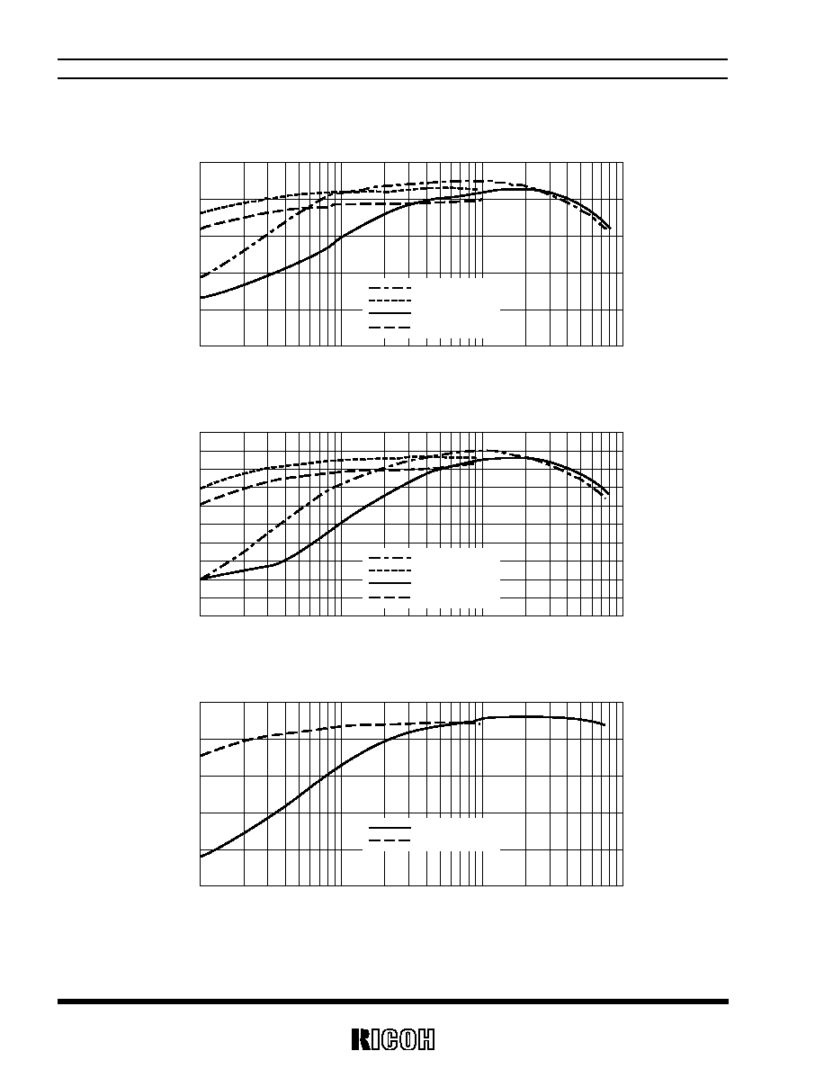
TYPICAL CHARACTERISTICS
1)
Output Voltage vs. Output Current
R1230D181E
Output Current(mA)
1.7
1
10
100
1000
1.9
1.85
1.75
1.8
Output Voltage(V)
V
IN
=3.3V PWM
V
IN
=3.3V VFM
V
IN
=5.0V PWM
V
IN
=5.0V VFM
R1230D181F
Output Current(mA)
1.7
1
10
100
1000
1.9
1.85
1.75
1.8
Output Voltage(V)
V
IN
=3.3V PWM
V
IN
=3.3V VFM
V
IN
=5.0V PWM
V
IN
=5.0V VFM
R1230D331F
Output Current(mA)
3.2
1
10
100
1000
3.4
3.35
3.25
3.3
Output Voltage(V)
V
IN
=5.0V PWM
V
IN
=5.0V VFM
R1230D
16
2)
Efficiency vs. Output Current
R1230D181E
Output Current(mA)
0
1
10
100
1000
100
60
80
20
40
Efficiency(%)
V
IN
=3.3V PWM
V
IN
=3.3V VFM
V
IN
=5.0V PWM
V
IN
=5.0V VFM
R1230D181F
Output Current(mA)
0
1
10
100
1000
100
70
60
80
90
10
20
30
40
50
Efficiency(%)
V
IN
=3.3V PWM
V
IN
=3.3V VFM
V
IN
=5.0V PWM
V
IN
=5.0V VFM
R1230D331F
Output Current(mA)
0
1
10
100
1000
100
60
80
20
40
Efficiency(%)
V
IN
=5.0V PWM
V
IN
=5.0V VFM

R1230D
17
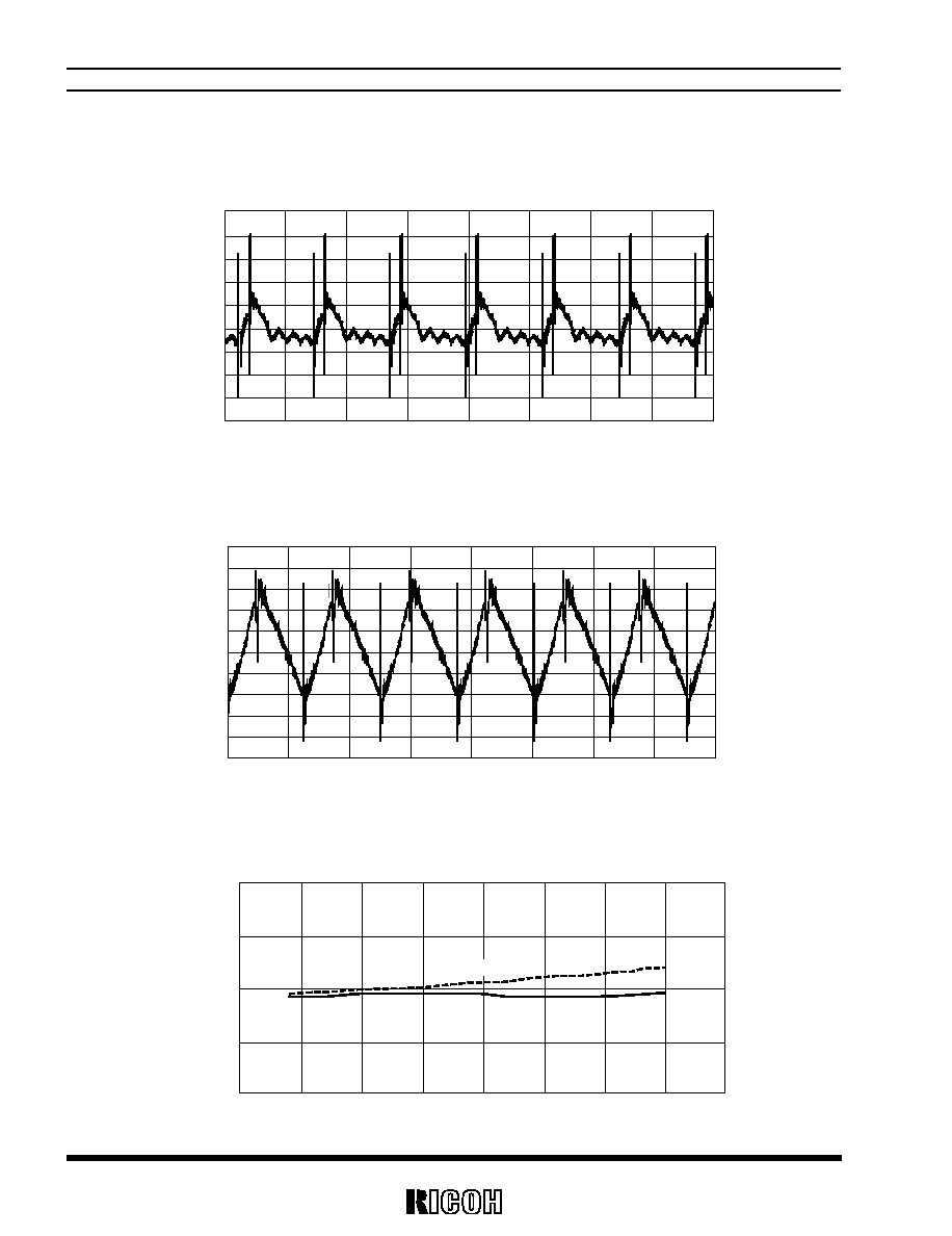
3)
Ripple Voltage vs. Output Current
R1230D181E
Time(sec)
-0.08
-1.00E-06 0.00E+00
0.06
0.04
0.02
-0.04
-0.02
0
-0.06
Output Ripple Voltage Vripple(V)
1.00E-06 2.00E-06 3.00E-06 4.00E-06 5.00E-06 6.00E-06 7.00E-06 8.00E-06
C
OUT
=10
µF Tantalum Capacitor ESR=400m
PWM Mode V
IN
=5.0V, I
OUT
=200mA
R1230D181F
Output Current I
OUT
(mA)
0
70
60
80
Output Ripple Voltage Vripple(V)
50
40
30
20
10
0
50
100
150
200
250
300
350
400
450
500
C
OUT
=10
µF, Tantalum Capacitor, ESR=400m
V
IN
=5.0V
V
IN
=3.3V
R1230D181F
Time(sec)
0.04
0.03
0.02
0.01
0
-0.01
-0.02
-0.03
-0.04
-1.00E-06 0.00E+00 1.00E-06 2.00E-06 3.00E-06 4.00E-06 5.00E-06 6.00E-06 7.00E-06 8.00E-06
Output Ripple Voltage Vripple(V)
C
OUT
=10
µF Ceramic Capacitor ESR=220m
PWM Mode V
IN
=5.0V, I
OUT
=200mA
R1230D
18
4)
Output Waveform
R1230D181F
Time(sec)
-0.04
-4.00E-06 -3.00E-06
0.05
0.04
0.02
0.03
-0.02
-0.01
0
0.01
-0.03
Output Ripple Voltage V
AC
(V)
PWM Mode V
IN
=5.0V, I
OUT
=10mA
-2.00E-06 -1.00E-06 0.00E+00 1.00E-06 2.00E-06 3.00E-06 4.00E-06
C
OUT
=10
µF Tantalum Capacitor ESR=400m
R1230D181F
Time(sec)
-0.06
-4.00E-06
-3.00E-06
0.04
0.03
0.02
0.01
0
-0.01
-0.02
-0.03
-0.04
-0.05
AC Output Voltage V
AC
(V)
-2.00E-06
-1.00E-06
0.00E+00
1.00E-06
2.00E-06
3.00E-06
4.00E-06
C
OUT
=10
µF Tantalum Capacitor ESR=400m
PWM Mode V
IN
=5.0V, I
OUT
=100mA
5)
Output Voltage vs. Input Voltage
R1230D181F
Input Voltage V
IN
(V)
1.70
1.85
1.90
Output Voltage V
OUT
(V)
1.80
1.75
2
2.5
3
3.5
4
4.5
5
5.5
6
I
OUT
=20mA
VFM
PWM

R1230D
19
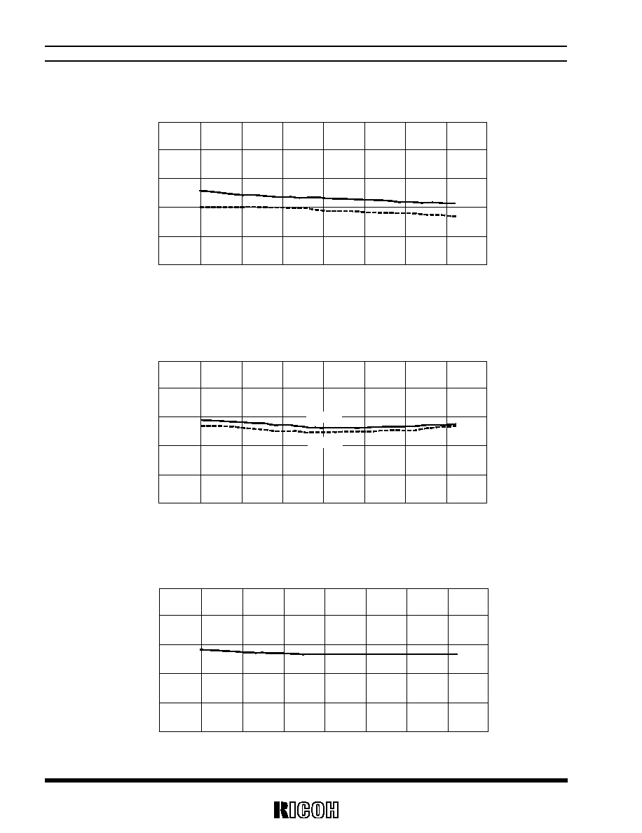
6)
Output Voltage vs. Temperature
R1230D181F
Temperature Topt(
∞C)
1.7
1.86
1.9
1.88
Output Voltage V
OUT
(V)
1.8
1.74
1.72
1.78
1.76
1.84
1.82
-60
-40
-20
0
20
40
60
80
100
I
OUT
=100mA
R1230D001G/H
Temperature Topt(
∞C)
0.70
0.85
0.90
Output Voltage V
OUT
(V)
0.80
0.75
-60
-40
-20
0
20
40
60
80
100
I
OUT
=100mA
7)
Oscillator Frequency vs. Temperature
Temperature Topt(
∞C)
300
800
900
600
700
400
500
1000
Frequency f
OSC
(kHz)
-60
-40
-20
0
20
40
60
80
100
V
IN
=V
OUT
+1.5V
R1230D
20
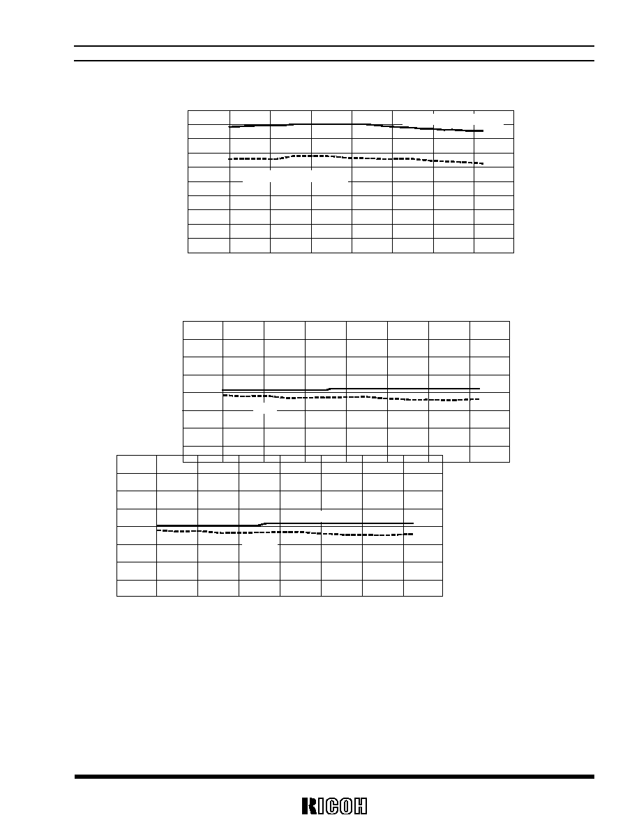
8)
Supply Current vs. Temperature
Temperature Topt(
∞C)
100
380
240
310
170
450
Supply Current I
SS
(
µ
A)
-60
-40
-20
0
20
40
60
80
100
V
IN
=5.5V
800kHz
500kHz
9)
Soft-start time vs. Temperature
R1230D181F
Temperature Topt(
∞C)
0
2.4
1.2
1.8
0.6
3.0
Soft-start Time Tsoft(ms)
-60
-40
-20
0
20
40
60
80
100
V
IN
=3.3V
800kHz
500kHz
10) Delay Time for protection vs. Temperature
R1230D181F
Temperature Topt(
∞C)
0
2.4
1.2
1.8
0.6
3.0
Delay Time for Protection
Circuit Tpre(ms)
-60
-40
-20
0
20
40
60
80
100
R1230D
21
11) UVLO Threshold/Released Voltage vs. Temperature
Temperature Topt(
∞C)
1.8
2.15
2.2
2.25
1.95
2
2.05
2.1
1.85
1.9
2.3
V
DD
Voltage Level(V)
-60
-40
-20
0
20
40
60
80
100
UVLO Detector Threshold
UVLO Released Voltage
12) CE Pin Input Voltage vs. Temperature
13) Mode Pin
Input
Voltage
vs. Tem-
perature
Temperature Topt(
∞C)
0
1.4
1.2
1.6
MODE Input Voltage
VMODE(V)
1.0
0.8
0.6
0.4
0.2
-60
-40
-20
0
20
40
60
80
100
MODEH
MODEL
Temperature Topt(
∞C)
0
1.4
1.2
1.6
Input Voltage V
CE
(V)
1.0
0.8
0.6
0.4
0.2
-60
-40
-20
0
20
40
60
80
100
CEH
CEL
R1230D
22
14) Duty Cycle at VFM Mode vs. Temperature
Temperature Topt(
∞C)
50
75
80
Duty Cycle at VFM Mode(%)
70
65
60
55
-60
-40
-20
0
20
40
60
80
100
15) Lx Transistor on Resistance vs. Temperature
Temperature Topt(
∞C)
0
0.75
1.00
ON Resistance Ron(
)
0.50
0.25
-60
-40
-20
0
20
40
60
80
100
V
IN
=3.0V
NchTr. On Resistance
PchTr. On Resistance
16) Limit Voltage vs. Temperature
Temperature Topt(
∞C)
0.10
0.45
0.40
0.50
Limit Voltage Vlimit(V)
0.35
0.30
0.25
0.20
0.15
-60
-40
-20
0
20
40
60
80
100

R1230D
23
17) Load Transient Response
R1230D181F
0.6
0.5
0.4
0.3
0.2
0.1
-0.1
-0.3
-0.2
-4.00E-05 -2.00E-05 0.00E+00 2.00E-05 4.00E-05 6.00E-05 8.00E-05 1.00E-04 1.20E-04 1.40E-04
V
IN
=5.0V PWM
0
Time(sec)
Load Current 100mA/div
AC Output Voltage V
AC
(V)
I
OUT
=0A
I
OUT
=100mA
R1230D181F
0.6
0.5
0.4
0.3
0.2
0.1
0
-0.1
-0.3
-0.2
-4.00E-05 -2.00E-05 0.00E+00 2.00E-05 4.00E-05 6.00E-05 8.00E-05 1.00E-04 1.20E-04 1.40E-04
V
IN
=5.0V PWM
Time(sec)
Load Current 100mA/div
Output Voltage V
AC
(V)
I
OUT
=0A
I
OUT
=200mA
R1230D181F
Time(sec)
0.6
0.5
0.4
0.3
0.2
0.1
0
-0.1
-0.3
-0.2
Load Current 100mA/div
AC Output Voltage V
AC
(V)
-4.00E-06 -1.00E-06 6.00E-06 1.10E-05 1.60E-05 2.10E-05 2.60E-05 3.10E-05 3.60E-05
V
IN
=5.0V PWM
I
OUT
=100mA
I
OUT
=0A

R1230D
24
R1230D181F
0.6
0.5
0.4
0.3
0.2
0.1
0
-0.1
-0.3
-0.2
0 0.0001 0.0002
0.0004
0.0006
0.0003
0.0005
0.0007 0.0008
-0.0002
-0.0001
V
IN
=5.0V PWM
Time(sec)
Load Current 100mA/div
AC Output Voltage V
AC
(V)
I
OUT
=100mA
I
OUT
=2mA
R1230D181F
Time(sec)
0.6
0.5
0.4
0.3
0.2
0.1
0
-0.1
-0.3
-0.2
Load Current 100mA/div
AC Output Voltage V
AC
(V)
-4.00E-06 -1.00E-06 6.00E-06 1.10E-05 1.60E-05 2.10E-05 2.60E-05 3.10E-05 3.60E-05
V
IN
=5.0V PWM
I
OUT
=200mA
I
OUT
=0A
R1230D181F
0.5
0.6
0.4
0.3
0.2
0.1
0
-0.1
-0.3
-0.2
0
0.0001 0.0002 0.0003 0.0004 0.0005 0.0006 0.0007 0.0008
-0.0002 -0.0001
V
IN
=5.0V PWM
Time(sec)
Load Current 100mA/div
AC Output Voltage V
AC
(V)
I
OUT
=200mA
I
OUT
=2mA

R1230D
25
18) Turn-on Waveform
R1230D181F
Time(sec)
-10
-8
-6
-4
-2
0
2
4
-1
0
1
2
3
4
5
CE Input Voltage V
CE
(V)
Output Voltage V
OUT
(V)
-0.0004
0
0.0004
0.0008
0.0012
0.0016
0.002
0.0024
0.0028
PWM Mode I
OUT
=0A V
IN
=5.0V
CE
V
OUT
R1230D181F
Time(sec)
-10
-8
-6
-4
-2
0
2
4
-1
0
1
2
3
4
5
CE Input Voltage V
CE
(V)
Output Voltage V
OUT
(V)
-0.0004
0
0.0004
0.0008
0.0012
0.0016
0.002
0.0024
0.0028
PWM Mode I
OUT
=50mA V
IN
=5.0V
CE
V
OUT
R1230D181F
Time(sec)
-10
-8
-6
-4
-2
0
2
4
-1
0
1
2
3
4
5
CE Input Voltage V
CE
(V)
Output Voltage V
OUT
(V)
-0.0004
0
0.0004
0.0008
0.0012
0.0016
0.002
0.0024
0.0028
PWM Mode I
OUT
=200mA V
IN
=5.0V
CE
V
OUT
R1230D
26
R1230D181F
Time(sec)
-10
-8
-6
-4
-2
0
2
4
-1
0
1
2
3
4
5
Output Voltage V
OUT
(V)
-0.0004
0
0.0004
0.0008
0.0012
0.0016
0.002
0.0024
0.0028
CE Input Voltage V
CE
(V)
VFM Mode I
OUT
=0A V
IN
=5.0V
CE
V
OUT
R1230D181F
Time(sec)
-10
-8
-6
-4
-2
0
2
4
-1
0
1
2
3
4
5
Output Voltage V
OUT
(V)
-0.0004
0
0.0004
0.0008
0.0012
0.0016
0.002
0.0024
0.0028
CE Input Voltage V
CE
(V)
VFM Mode I
OUT
=50mA V
IN
=5.0V
CE
V
OUT