
NO. EA-076-0012
Negative Output Charge Pump
Regulator (100mA)
R1250V◊◊1A SERIES
APPLICATION MANUAL

Negative Output Charge
Pump Regulator (100mA)
R1250V◊◊1A SERIES
1
OUTLINE
The R1250V◊◊1A Series are Negative Output Charge Pump Regulator ICs, which can be developed as local power
suppliers for portable appliances and small electric appliances used with batteries, with low supply current by CMOS
process.
Each of these ICs consists of an oscillator, a control circuit, a reference voltage unit, an error amplifier, and an out-
put driver circuit. The R1250V◊◊1A can easily supply negative voltage, or regulated setting output voltage in the
range from -2V to -4V from positive input voltage.
The chip enable function works to shut down the internal circuit and reduces supply current at the stand-by mode,
therefore the R1250V◊◊1A is very suitable for the application such as portable systems that require low supply cur-
rent.
Since the package for this IC is TSSOP8 package (TSOP8 in EIAJ standard), high density mounting of the ICs on
board is possible.
FEATURES
∑ Output Current..................... 100mA (MAX. at V
IN
=5.0V, C
IN
=C
P
=C
OUT
=4.7µF, Set Output Voltage=-3.0V)
∑ Output Voltage Accuracy...... ±3.0% (V
IN
=5.0V, C
IN
=C
P
=C
OUT
=4.7µF, Set Output Voltage=-3.0V, I
OUT
=0mA/10mA)
±9.0% (V
IN
=5.0V, C
IN
=C
P
=C
OUT
=4.7µF, Set Output Voltage=-3.0V, I
OUT
=50mA)
∑ Output Voltage...................... Stepwise setting with a step of 0.1V in the range from -2.0V to -4.0V is possible.
∑ Range of Input Voltage ......... V
OUT
V to +5.5V (Set Output Voltage=-4.0V to -2.8V)
+2.7V to +5.5V (Set Output Voltage=-2.7V to -2.0V)
∑ Oscillator Frequency ............ TYP. 280kHz
∑ Chip Enable Function (Active at "L")
∑ Package ................................. TSSOP8
APPLICATIONS
∑ Power source for Disk Drives.
∑ Power source for hand-held communication equipment and battery-powered equipment.
∑ Power source for PC peripherals and ADD-ON cards.
∑ Power source for portable audio-visual appliances such as cameras.
∑ Local power source for small electrical appliances.
R1250V◊◊1A
2
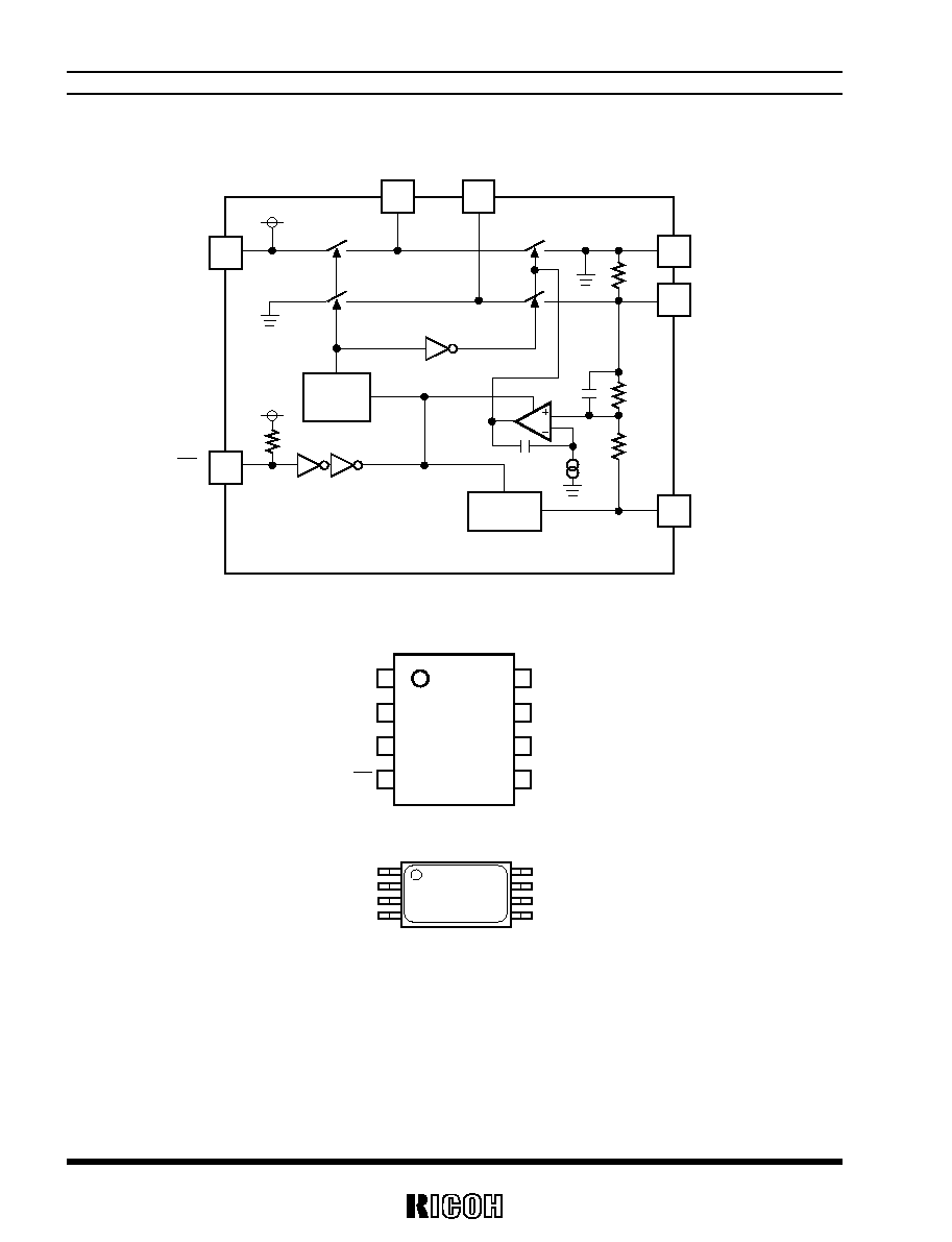
BLOCK DIAGRAM
V
IN
V
OUT
1
3
2
7
6
SW1
SW3
SW4
SW2
8
4
GND
CE
R
O
R
PU
OSC
Vref
Vref
C
P+
C
P-
PIN CONFIGURATION
TSSOP8
1
3
2
4
C
P+
C
P
-
GND
CE
8
6
7
5
V
IN
Vref
V
OUT
NC
PACKAGE DIMENSION
1
2
3
4
8
7
6
5
R1250V◊◊1A
3
PIN DESCRIPTION
Pin No.
Symbol
Description
1
C
P+
C
P
(Capacitor for Charge Pump) Positive Power Supply Pin
2
GND
Ground Pin
3
C
P-
C
P
(Capacitor for Charge Pump) Negative Power Supply Pin
4
----
CE
Chip Enable Pin (active at "L")
5
NC
No Connection Pin
6
Vref
Output Pin for Reference Voltage
(*Note1)
7
V
OUT
Output Pin for Negative Regulator
8
V
IN
Power Supply Pin
*Note1
Vref is just a monitoring pin, therefore remain open. Do not connect any load. Refer to Techni-
cal Notes.
ABSOLUTE MAXIMUM RATINGS
(GND=0V)
Symbol
Item
Rating
Unit
V
IN
V
IN
Supply Voltage
-0.3 to 7.5
V
V
CE
----
CE Pin Input Voltage
-0.3 to V
IN
+0.3
V
V
P+
C
P+
Pin Input Voltage
-0.3 to V
IN
+0.3
V
Vref
Vref Pin Voltage
-0.3 to V
IN
+0.3
V
V
P-
C
P
- Pin Input Voltage
V
IN
-12 to +0.3
V
V
OUT
V
OUT
Pin Voltage
V
IN
-12 to +0.3
V
I
OUT
Output Current
200
mA
P
D
Power Dissipation
*NOTE1
490
mW
Topt
Operating Temperature Range
-40 to +85
∞C
Tstg
Storage Temperature Range
-55 to +125
∞C
*Note1: Power dissipation is specified under the specified condition.
Conditions;
Evaluation Board Dimensions: 50mm
◊ 50mm ◊ 1.6mm
Material: Glass Epoxy (FR-4)
Reverse side of the evaluation board: Plane Copper
Surface of the evaluation board: Land pattern and Wiring
R1250V◊◊1A
4
SELECTION GUIDE
The output voltage and the active type for the ICs can be selected at the user's request.
The selection can be made with designating the part number as shown below;
R1250V◊◊1A-◊◊
a b c
Code
Contents
a
Setting Output Voltage
◊◊: The absolute value of Output Voltage
Stepwise setting with a step of 0.1V in the range of -2.0V to -4.0V is possible.
b
Designation of Active Type of the Chip Enable Circuit:
A (fixed) : "L" active type
c
Designation of Packing Type
E2 : E2 1reel=2000pcs
R1250V◊◊1A
5
ELECTRICAL CHARACTERISTICS
R1250V
◊◊1A
(Unless otherwise provided, V
IN
=5.0V, Topt=25∞C, C
P
, C
OUT
= Ceramic 4.7µF)
Symbol
Item
Conditions
MIN.
TYP.
MAX.
Unit
Set Output Voltage = -2.7V to -2.0V
2.7
V
IN
Operating Input Voltage
Set Output Voltage = -4.0V to -2.8V
|Set V
OUT
|
5.5
V
-2.4V to -2.0V
1.50
2.30
-2.9V to -2.5V
1.60
2.55
-3.4V to -3.0V
1.70
2.75
I
SS
Supply Current
Operation: Active,
for IC itself
*Note1
-4.0V to -3.5V
1.80
3.00
mA
I
STB
Shut-down Current
Operation: Shut-down, for IC
itself
*Note2
0.1
1
µA
-2.4V to -2.0V
◊0.95
◊1.05
-2.9V to -2.5V
◊0.96
◊1.04
-3.4V to -3.0V
◊0.97
◊1.03
I
OUT
=0mA/10mA
-4.0V to -3.5V
◊0.97
◊1.03
I
OUT
=50mA
-2.4V to -2.0V
◊0.88
◊1.12
-2.9V to -2.5V
◊0.89
◊1.11
-3.4V to -3.0V
◊0.91
◊1.09
V
OUT
Output Voltage
I
OUT
=75mA
-4.0V to -3.5V
◊0.92
◊1.08
V
Vref
Reference Voltage
*Note3
No load
V
OUT
V
I
OUT
=10mA to 50mA -2.4V to -2.0V
V
OUT
/
I
OUT
Load Regulation
I
OUT
=10mA to 75mA -4.0V to -2.5V
0.7
mV/
mA
fosc
Oscillator Frequency
Output Frequency
238
280
322
kHz
fosc/T
Oscillator Frequency
Temperature Coefficient
±0.25
kHz/
∞C
Duty
Oscillator Duty Cycle
At no Load
50
%
V
SDH
CE "H" Input Voltage
1.5
V
V
SDL
CE "L" Input Voltage
0.25
V
R
PU
CE Pull-up Resistance
0.68
1.25
3.00
M
R
O
Resistance between
V
OUT
and GND
5
k
*Note1
Refer to Test Circuit 1.
*Note2:
Refer to Test Circuit 6.
*Note3:
Do not connect ant load. Refer to Technical Notes.
*Use Ceramic Capacitors with low ESR. Capacitors with high ESR could have bad effect on the performance of this IC.
R1250V◊◊1A
6
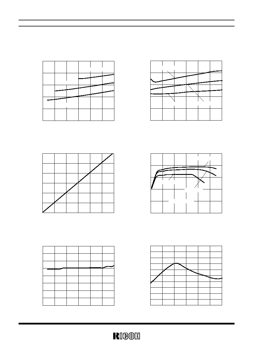
TYPICAL CHARACTERISTICS
1)
Supply Current at no load vs. Input Voltage
2)
Supply Current at no load vs. Temperature
R1250V
◊◊
◊◊
◊◊
◊◊1A
R1250V
◊◊
◊◊
◊◊
◊◊1A
2.000
2.500
1.500
1.000
0.500
0.000
Input Voltage V
IN
(V)
2.5
3.0
-3.0V Output
-2.0V Output
-4.0V Output
4.0
5.0
4.5
5.5
3.5
Supply Current at no load I
SS2
(mA)
2.0
2.5
1.5
1.0
0.5
0.0
Temperature Topt (
∞C)
-50
-25
-3.0V Output
-2.0V Output
-4.0V Output
25
75
50
100
0
Supply Current at no load I
SS2
(mA)
3)
Input Current vs. Output Load Current
4)
Efficiency vs. Load Current
R1250V301A
R1250V
◊◊
◊◊
◊◊
◊◊1A
100
120
80
60
40
20
0
Output Load Current I
OUT
(mA)
0
20
60
100
80
120
40
Input Current I
IN
(mA)
80
100
60
40
20
0
0
20
-3.0V Output
-2.0V Output
-4.0V Output
V
IN
=lOutputl+1V
60
100
80
120
40
Efficiency
(%)
Output Load Current I
OUT
(mA)
5)
Oscillator Frequency vs. Input Voltage
6)
Oscillator Frequency vs. Temperature
R1250V201A
R1250V201A
310
300
320
290
280
270
260
250
240
Input Voltage V
IN
(V)
2.5
3
4
5
4.5
5.5
3.5
Oscillator F
requency f
osc (kHz)
Temperature Topt (
∞C)
298
296
294
300
292
290
288
286
284
282
280
-50
-25
25
75
50
100
0
Oscillator F
requency f
osc (kHz)

R1250V◊◊1A
7
7)
Output Voltage vs. Output Load Current
R1250V201A
R1250V201A
-1.9
-2
-2.1
Output Load Current I
OUT
(mA)
0
20
60
100
80
120
40
Output
V
oltage
V
OUT
(V)
V
IN
=5.0V
85
∞C
50
∞C
25
∞C
Output Load Current I
OUT
(mA)
Output
V
oltage
V
OUT
(V)
85
∞C
50
∞C
25
∞C
V
IN
=3.0V
-1.6
-1.7
-1.5
-1.8
-1.9
-2
-2.1
-2.2
0
20
60
100
80
120
40
R1250V301A
R1250V301A
-2.9
-3
-3.1
Output Load Current I
OUT
(mA)
0
20
60
100
80
120
40
Output
V
oltage
V
OUT
(V)
85
∞C
50
∞C
25
∞C
V
IN
=5.0V
Output Load Current I
OUT
(mA)
Output
V
oltage
V
OUT
(V)
85
∞C
50
∞C
25
∞C
V
IN
=4.0V
-2.6
-2.7
-2.5
-2.8
-2.9
-3
-3.1
-3.2
0
20
60
100
80
120
40
R1250V401A
Output Voltage Load Current I
OUT
(mA)
Output
V
oltage
V
OUT
(V)
85
∞C
50
∞C
25
∞C
V
IN
=5.0V
-3.6
-3.7
-3.5
-3.8
-3.9
-4
-4.1
-4.2
0
20
60
100
80
120
40

R1250V◊◊1A
8
8)
Output Voltage vs. Temperature
R1250V201A
R1250V301A
-1.99
-1.98
-2.00
-2.01
-2.02
Temperature Topt (
∞C)
-50
-25
25
75
50
100
0
Output
V
oltage
V
OUT
(V)
-3.05
-3.03
-3.03
-3.02
-3.01
-3.00
-2.99
Temperature Topt (
∞C)
-50
-25
25
75
50
100
0
Output
V
oltage
V
OUT
(V)
R1250V401A
-4.06
-4.05
-4.04
-4.03
-4.02
-4.01
-4.00
-3.99
-3.98
Temperature Topt (
∞C)
-50
-25
25
75
50
100
0
Output
V
oltage
V
OUT
(V)
9)
Output Voltage Waveform
-3.00V
100mV
1.00
µs
Unless otherwise provided, conditions are as follows;
Sample: R1250V301A
V
IN
=5.0V
C
IN
=C
P
=C
OUT
=4.7µF
I
OUT
=0mA
BW=20MHz

R1250V◊◊1A
9
-3.00V
100mV
1.00
µs
I
OUT
=10mA
-3.00V
100mV
1.00
µs
I
OUT
=50mA
TEST CIRCUITS
Test Circuit 1) Supply Current 1
Test Circuit 2) Typical Characteristics 1), 2)
Test Circuit 3) Typical Characteristics 3), 4), 7), 8)
Test Circuit 4) Typical Characteristics 5), 6)
Test Circuit 5) Typical Characteristics 9)
Test Circuit 6) Standby Current
1)
Test Circuit 1
A
A
5.5V
I
SS
-P
I
SS
-N
Set Output Voltage+0.2V
1.C
P+
3.C
P
-
2.GND
4.CE
8.V
IN
6.Vref
7.V
OUT
5.NC
<Definition> I
SS1
=I
SS
-P+I
SS
-N
(*)
To stabilize voltage, a few µF bypass capacitors are applied to V
OUT
pin and V
IN
pin.

R1250V◊◊1A
10
2)
Test Circuit 2
A
4.7
µF
4.7
µF
4.7
µF
1.C
P+
3.C
P-
2.GND
4.CE
8.V
IN
6.Vref
7.V
OUT
5.NC
I
SS2
3)
Test Circuit 3
V
A
4.7
µF
4.7
µF
4.7
µF
1.C
P+
3.C
P-
2.GND
4.CE
8.V
IN
6.Vref
7.V
OUT
5.NC
I
IN
I
OUT
<Definition> (|V
OUT
|◊I
OUT
)/(V
IN
◊I
IN
)◊100(%)
4)
Test Circuit 4
1.C
P+
3.C
P-
2.GND
4.CE
8.V
IN
6.Vref
7.V
OUT
5.NC
Oscilloscope
(*)
To stabilize voltage, a few µF bypass capacitor is applied to V
IN
pin.

R1250V◊◊1A
11
5)
Test Circuit 5
A
4.7
µF
4.7
µF
4.7
µF
1.C
P+
3.C
P-
2.GND
4.CE
8.V
IN
6.Vref
7.V
OUT
5.NC
I
IN
I
OUT
Oscilloscope
BW:20MHz
5.0V
6)
Test Circuit 6
A
7.5V
1.C
P+
3.C
P-
2.GND
4.CE
8.V
IN
6.Vref
7.V
OUT
5.NC
TYPICAL APPLICATION
4.7
µF
4.7
µF
Output
C
P+
C
P-
GND
CE
V
IN
Vref
V
OUT
NC
Open
C
P
C
IN
C
OUT
4.7
µF
(*)
Vref pin should not be wired. Refer to Technical Notes.

R1250V◊◊1A
12
OPERATION
1)
Basic Operation
The R1250V◊◊1A Series make SW1 through SW4 ON and OFF by the clock generated by internal oscillator (OSC)
with fixed frequency, and operate as a inverting charge pump with the capacitor C
P
and the capacitor C
OUT
.
The Output Voltage is feedback and the voltage between the Output Voltage and Reference Voltage (Vref =V
OUT
V) is divided half, and it is compared with the GND (=0V) level by an internal operational amplifier.
By this action, the impedance of SW3 is controlled to correspond with its load current and Output Voltage keeps
"Set V
OUT
" level.
2)
Status of Internal Circuits at Standby mode and Standby Current
At Standby mode, R1250V Series keep the voltage of C
P
as shown below:
V
IN
C
IN
C
P
R
O
R
OUT
C
OUT
V
OUT
up to 5k
R1250V
◊◊1A
When you design a system with using this IC, consider the following subjects;
2-(1) If very small leakage current would be a critical, the leakage current of both C
IN
and C
P
should be considered.
2-(2) Because the voltage level of C
P
keeps as much as V
DD
level, the speed for start-up from stand-by mode is faster
than the start-up by power-on.
2-(3) V
OUT
is internally pulled down through 5k to GND. Time constant "" of transient response (turn-off speed) of
V
OUT
can be calculated as follows:
(5[k] R
OUT
) ◊ C
OUT
(R
OUT
: Output load resistance)
2-(4) Load current should be OFF synchronously with this IC if the load is electronic or connected between V
IN
and
V
OUT
. If some charge is continuously flown to the Output V
OUT
at the "OFF" state, the voltage level of V
OUT
will
rise and could be beyond 0V. And if the voltage will be +0.3V (that is designated as absolute maximum rating.),
this IC might be break down.
3)
Ripple Voltage
Ripple voltage of Output waveform can be roughly calculated as follows:
Vripple [mVp-p] 0.5◊ (I
OUT
[mA] + Supply Current at no load [mA]) / (Oscillator Frequency: 280000 [Hz])
/ C
OUT
[F]
Supply Current at no load [mA] Supply Current 1 [mA]

R1250V◊◊1A
13
4)
Power Consumption
Power Consumption at large load current of this IC can be calculated as follows:
Wchip [mW] (V
IN
[V]-| Set Output Voltage |) ◊ (I
OUT
[mA])
TECHNICAL NOTES
To use this IC, the following things should be considered.
1) Short Protection function for each pin is not included in this IC.
2) Use capacitors with low equivalent series resistor (ESR) for C
IN
, C
P
, C
OUT
pins. Capacitors with large ESR make
this IC's performance worse.
3) Make wiring of GND, V
IN
, C
P+
, C
P-
secure enough and decrease impedance. High impedance could be a cause of
unstable operation of this IC.
4) When this IC is used with large load current, consider its radiation of heat.
5) Basically, Vref pin can be used for soldering to the mount pad of PCB. Do not make it wiring.
6) Load type is electronic or setting between V
IN
and V
OUT
, in cases of OFF-state of this IC and start-up state of this
IC, make sure not to raise V
OUT
level on positive voltage side. If the voltage level is beyond +0.3V, which is desig-
nated as the absolute maximum rating, this IC could be broken.