2CH PWM DC/DC CONTROLLER
R1280D002x SERIES
1
R1280D_E.doc/2003/05/23
NO. EA-086-0305
OUTLINE
The R1280D002x Series are CMOS-based 2-channel PWM Step-up (as Channel 1)/Inverting (as Channel 2) DC/DC
converter controllers.
Each of the R1280D002x Series consists of an oscillator, a PWM control circuit, a reference voltage unit, an error
amplifier, a reference current unit, a protection circuit, and an under voltage lockout (UVLO) circuit. A high efficiency
Step-up/Inverting DC/DC converter can be composed of this IC with inductors, diodes, power MOSFETs, resisters,
and capacitors. Each Output Voltage can be adjustable with external resistors, while soft-start time can be adjustable
with external capacitors.
Maximum Duty Cycle of R1280D002A and C series can be also adjustable with external resistors.
Maximum Duty Cycle of R1280D002B is built-in as 90%(Typ.).
When CE pin of R1280D002B is set at GND level, this IC turns off external power MOSFETs of Step-up/Inverting
as Standby-mode.
Standby current is typically 0µA.
As for a protection circuit, if Maximum duty cycle of either Step-up DC/DC converter side or Inverting DC/DC
converter side is continued for a certain time, the R1280D Series latch both external drivers with their off state by its
Latch-type protection circuit. Delay time for protection is internally fixed typically at 100ms. To release the protection
circuit, restart with power-on (Voltage supplier is equal or less than UVLO detector threshold level), or as for
R1280D002B, once after making the circuit be stand-by with chip enable pin and enable the circuit again.
FEATURES
∑ Input Voltage Range .....................................................2.5V to 5.5V
∑ Built-in Latch-type Protection Function by monitoring duty cycle (Fixed Delay Time Typ. 100ms)
∑ Oscillator Frequency ....................................................700kHz (R1280D002A,B)/200kHz (R1280D002C)
∑ Maximum Duty Cycle ..................................................Typ. 90% (Only applied to R1280D002B Series)
∑ High Reference Voltage Accuracy ...............................±1.5%
∑ U.V.L.O. Threshold .......................................................Typ. 2.2V (Hysteresis: Typ. 0.1V)
∑ Small Package...............................................................thin SON-10 (package thickness Max. 0.9mm)
APPLICATIONS
∑ Constant Voltage Power Source for Portable Equipment.
∑ Constant Voltage Power Source for LCD and CCD.
R1280D002x
2
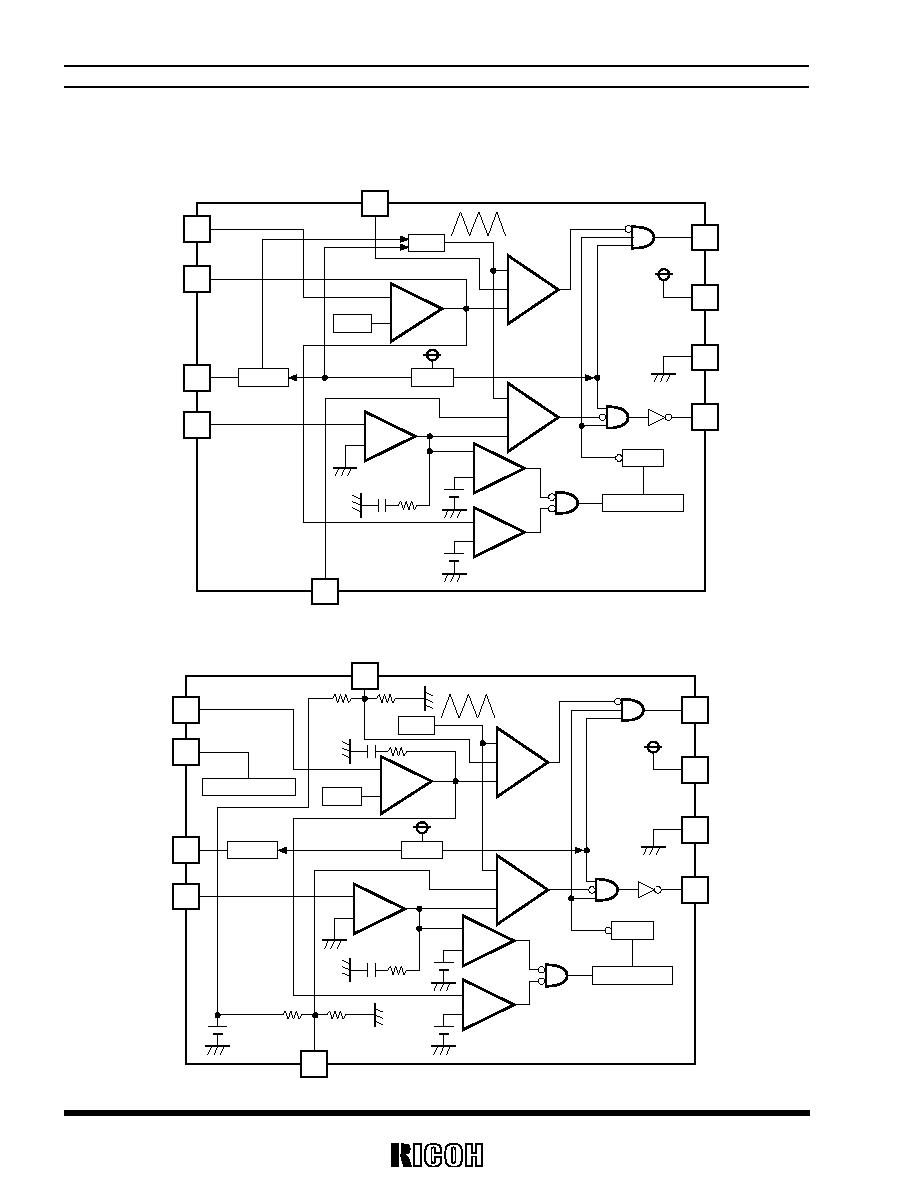
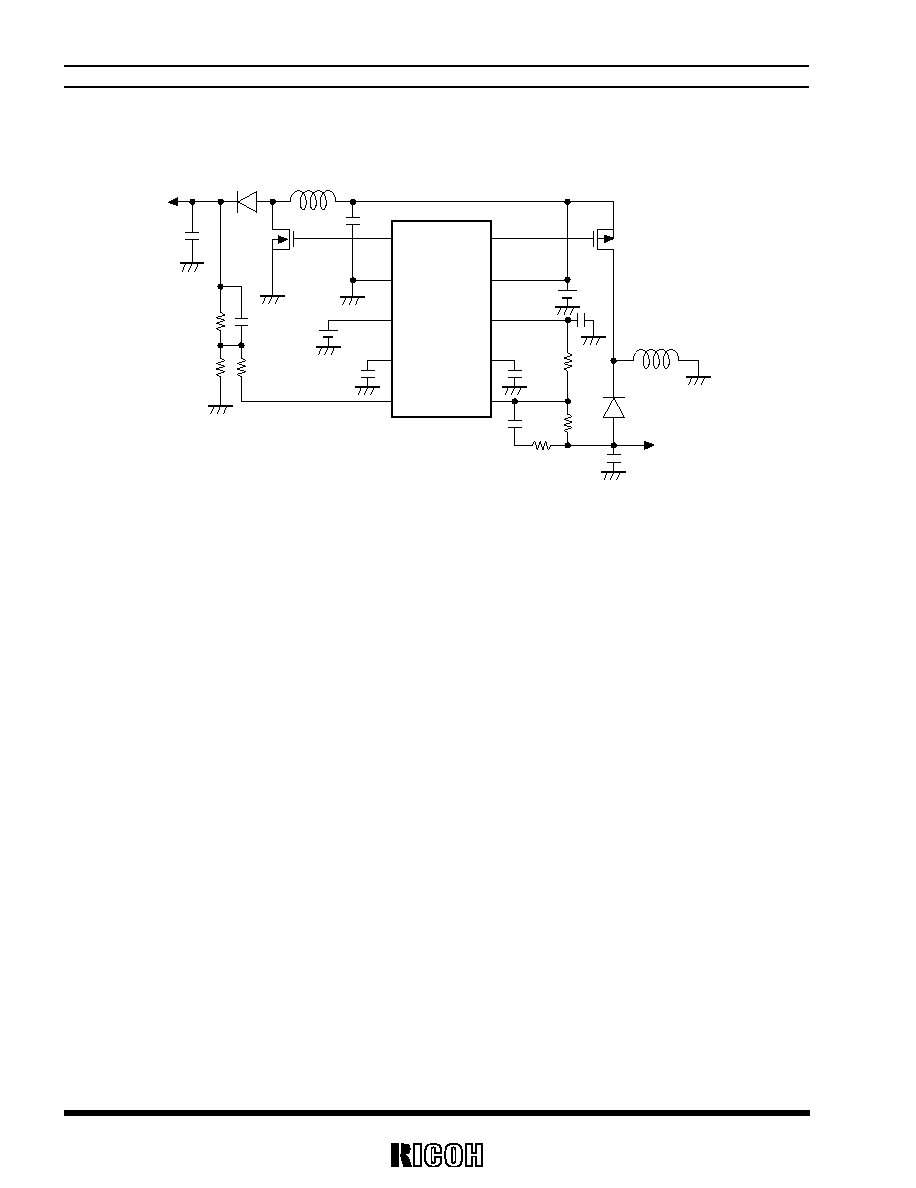
BLOCK DIAGRAM
∑ R1280D002A/C
V
FB1
AMPOUT1
Vrefout
V
FB2
EXT1
V
IN
GND
EXT2
DTC2
Vrefout
CH2
CH1
Vref1
OSC
UVLO
Latch
Delay Circuit
-
-
+
-
-
+
-
+
-
+
-
+
+
-
DTC1
∑ R1280D002B
V
FB1
C
E
Vrefout
V
FB2
EXT1
V
IN
GND
EXT2
DTC2
Vrefout
CH2
CH1
Vref1
OSC
UVLO
Latch
Delay Circuit
CHIP ENABLE
-
-
+
-
-
+
-
+
+
-
-
+
+
-
DTC1

R1280D002x
3
SELECTION GUIDE
The mask option for the ICs can be selected at the user's request. The selection can be made with designating the
part number as shown below;
R1280D002x-TR
Part Number
a b
Code
Contents
a
Designation of Mask Option :
A version: fosc=700kHz, with External Phase Compensation for Channel 1.
B version: fosc=700kHz, with Internal Phase Compensation and standby mode.
C version: fosc=200kHz, with External Phase Compensation for Channel 1
b
Designation of Taping Type :
(Refer to Taping Specifications.)
PIN CONFIGURATION
SON10
(mark side)
10
6
7
8
9
1
5
4
3
2
R1280D002x
4
PIN DESCRIPTION
∑ R1280D002A/C
Pin No.
Symbol
Description
1
EXT1
External Transistor of Channel 1 Drive Pin (CMOS Output)
2
GND
Ground Pin
3
AMPOUT1
Amplifier Output Pin of Channel 1
4
DTC1
Maximum Duty Cycle of Channel 1 Setting Pin
5
V
FB1
Feedback pin of Channel 1
6
V
FB2
Feedback pin of Channel 2
7
DTC2
Maximum Duty Cycle of Channel 2 Setting Pin
8
Vrefout
Reference Output Pin
9
V
IN
Voltage Supply Pin of the IC
10
EXT2
External Transistor of Channel 2 Drive Pin (CMOS Output)
∑ R1280D002B
Pin No.
Symbol
Description
1
EXT1
External Transistor of Channel 1 Drive Pin (CMOS Output)
2
GND
Ground Pin
3
CE
Chip Enable Pin
4
DTC1
Soft-start Time of Channel 1 Setting Pin
5
V
FB1
Feedback pin of Channel 1
6
V
FB2
Feedback pin of Channel 2
7
DTC2
Soft-start Time of Channel 2 Setting Pin
8
Vrefout
Reference Output Pin
9
V
IN
Voltage Supply Pin of the IC
10
EXT2
External Transistor of Channel 2 Drive Pin (CMOS Output)
R1280D002x
5
ABSOLUTE MAXIMUM RATINGS
∑ R1280D002A/C
Symbol
Item
Rating
Unit
V
IN
V
IN
Pin Voltage
6.5
V
V
EXT1,2
V
EXT1,2
Pin Output Voltage
-0.3~V
IN
+0.3
V
V
AMPOUT1
AMPOUT1 Pin Voltage
-0.3~V
IN
+0.3
V
V
DTC1,2
DTC1,2 Pin Voltage
-0.3~V
IN
+0.3
V
V
refout
V
REFOUT
Pin Voltage
-0.3~V
IN
+0.3
V
V
FB1,2
V
FB1
,V
FB2
Pin Voltage
-0.3~V
IN
+0.3
V
I
EXT1,2
EXT1,2 Pin Output Current
±50
mA
P
D
Power Dissipation
250
mW
Topt
Operating Temperature Range
-40 to +85
∞C
Tstg
Storage Temperature Range
-55 to +125
∞C
∑ R1280D002B
Symbol
Item
Rating
Unit
V
IN
V
IN
Pin Voltage
6.5
V
V
EXT1,2
V
EXT1,2
Pin Output Voltage
-0.3~V
IN
+0.3
V
V
CE
CE Pin Voltage
-0.3~V
IN
+0.3
V
V
DTC1,2
DTC1,2 Pin Voltage
-0.3~V
IN
+0.3
V
V
refout
V
REFOUT
Pin Voltage
-0.3~V
IN
+0.3
V
V
FB1,2
V
FB1
,V
FB2
Pin Voltage
-0.3~V
IN
+0.3
V
I
EXT1,2
EXT1,2 Pin Output Current
±50
mA
P
D
Power Dissipation
250
mW
Topt
Operating Temperature Range
-40 to +85
∞C
Tstg
Storage Temperature Range
-55 to +125
∞C

R1280D002x
6
ELECTRICAL CHARACTERISTICS
∑ R1280D002A
Topt=25∞C
Symbol
Item
Conditions
Min.
Typ.
Max.
Unit
V
IN
Operating Input Voltage
2.5
5.5
V
V
REFOUT
V
REFOUT
Voltage Tolerance
V
IN
=3.3V, I
OUT
=1mA
1.478
1.500
1.522
V
I
ROUT
V
REFOUT
Output Current
V
IN
=3.3V
20
mA
V
REFOUT
/V
IN
V
REFOUT
Line Regulation
2.5V V
IN
5.5V
2
6
mV
V
REFOUT
/I
OUT
V
REFOUT
Load Regulation
1mA I
ROUT
10mA V
IN
=3.3V
6
12
mV
I
LIM
V
REFOUT
Short Current Limit
V
IN
=3.3V, V
REFOUT
=0V
25
mA
V
REFOUT
/T V
REFOUT
Voltage Temperature Coefficient
-40∞C Topt 85∞C
±150
ppm/∞C
V
FB1
V
FB1
Voltage
V
IN
=3.3V
0.985
1.000
1.015
V
V
FB1
/T
V
FB1
Voltage Temperature Coefficient
-40∞C Topt 85∞C
±150
ppm/∞C
I
FB1,2
I
FB1,2
Input Current
V
IN
=5.5V,V
FB1
or V
FB2
=0V or 5.5V
-0.1
0.1
µA
f
OSC
Oscillator Frequency
EXT1,2 Pins at no load, V
IN
=3.3V
595
700
805
kHz
I
DD1
Supply Current
V
IN
=5.5V, EXT1,2 pins at no load
1.4
3.0
mA
R
EXTH1
EXT1 "H" ON Resistance
V
IN
=3.3V, I
EXT
=-20mA
4.0
8.0
R
EXTL1
EXT1 "L" ON Resistance
V
IN
=3.3V, I
EXT
=20mA
2.7
5.0
R
EXTH2
EXT2 "H" ON Resistance
V
IN
=3.3V, I
EXT
=-20mA
4.0
8.0
R
EXTL2
EXT2 "L" ON Resistance
V
IN
=3.3V, I
EXT
=20mA
3.7
8.0
T
DLY
Delay Time for Protection
V
IN
=3.3V, V
FB1
=1.1V0V
60
100
140
ms
V
UVLOD
UVLO Detector Threshold
2.10
2.20
2.35
V
V
UVLO
UVLO Released Voltage
V
UVLOD
+0.10
2.45
V
V
DTC10
CH1 Duty=0%
V
IN
=3.3V
0.1
0.2
0.3
V
V
DTC1100
CH1 Duty=100%
V
IN
=3.3V
1.1
1.2
1.3
V
V
DTC20
CH2 Duty=0%
V
IN
=3.3V
0.1
0.2
0.3
V
V
DTC2100
CH2 Duty=100%
V
IN
=3.3V
1.1
1.2
1.3
V
A
V1
CH1 Open Loop Gain
V
IN
=3.3V
110
dB
F
T1
CH1 Single Gain Frequency Band
V
IN
=3.3V, A
V1
=0dB
1.9
MHz
V
ICR1
CH1 Input Voltage Range
V
IN
=3.3V
0.7 to V
IN
V
I
AMPL
CH1 Sink Current
V
IN
=3.3V, V
AMPOUT1
=1.0V,
V
FB1
=V
FB1
+ 0.1V
70
115
µA
I
AMPH
CH1 Source Current
V
IN
=3.3V, V
AMPOUT1
=1.0V,
V
FB1
=V
FB1
- 0.1V
-1.4
-0.7
mA
A
V2
CH2 Open Loop Gain
V
IN
=3.3V
60
dB
F
T1
CH2 Single Gain Frequency Band
V
IN
=3.3V, AV2=0dB
3
MHz
V
ICR1
CH2 Input Voltage Range
V
IN
=3.3V
-0.2 to
V
IN
-1.3
V
V
FB2
CH2 Input Offset Voltage
V
IN
=3.3V
-12
12
mV
R1280D002x
7
∑ R1280D002B
Topt=25∞C
Symbol
Item
Conditions
Min.
Typ.
Max.
Unit
V
IN
Operating Input Voltage
2.5
5.5
V
V
REFOUT
V
REFOUT
Voltage Tolerance
V
IN
=3.3V, I
OUT
=1mA
1.478
1.500
1.522
V
I
ROUT
V
REFOUT
Output Current
V
IN
=3.3V
20
mA
V
REFOUT
/V
IN
V
REFOUT
Line Regulation
2.5V V
IN
5.5V
2
6
mV
V
REFOUT
/I
OUT
V
REFOUT
Load Regulation
1mA I
ROUT
10mA V
IN
=3.3V
6
12
mV
I
LIM
V
REFOUT
Short Current Limit
V
IN
=3.3V, V
REFOUT
=0V
25
mA
V
REFOUT
/T
V
REFOUT
Voltage Temperature Coeffi-
cient
-40∞C Topt 85∞C
±150
ppm/∞C
V
FB1
V
FB1
Voltage
V
IN
=3.3V
0.985
1.000
1.015
V
V
FB1
/T
V
FB1
Voltage Temperature Coefficient
-40∞C Topt 85∞C
±150
ppm/∞C
I
FB1,2
I
FB1,2
Input Current
V
IN
=5.5V,V
FB1
or V
FB2
=0V or 5.5V
-0.1
0.1
µA
f
OSC
Oscillator Frequency
EXT1,2 Pins at no load, V
IN
=3.3V
595
700
805
kHz
I
DD1
Supply Current
V
IN
=5.5V, EXT1,2 pins at no load
1.4
3.0
mA
Maxdty
Maximum Duty Cycle
V
IN
=3.3V, C
DTC1
,
2
=1000pF
84
90
95
%
R
EXTH1
EXT1 "H" ON Resistance
V
IN
=3.3V, I
EXT
=-20mA
4.0
8.0
R
EXTL1
EXT1 "L" ON Resistance
V
IN
=3.3V, I
EXT
=20mA
2.7
5.0
R
EXTH2
EXT2 "H" ON Resistance
V
IN
=3.3V, I
EXT
=-20mA
4.0
8.0
R
EXTL2
EXT2 "L" ON Resistance
V
IN
=3.3V, I
EXT
=20mA
3.7
8.0
T
DLY
Delay Time for Protection
V
IN
=3.3V, V
FB1
=1.1V0V
60
100
140
ms
T
SS1
Soft Start Time1 for Ch1
V
IN
=3.3V, C
DTC1
=0.33µF
10
ms
T
SS2
Soft Start Time2 for Ch2
V
IN
=3.3V, C
DTC2
=0.33µF
15
ms
V
CEH
CE "H" Input Voltage
V
IN
=5.5V
1.5
V
V
CEL
CE "L" Input Voltage
V
IN
=2.5V
0.3
V
V
UVLOD
UVLO Detector Threshold
2.10
2.20
2.35
V
V
UVLO
UVLO Released Voltage
V
UVLOD
+0.10
2.45
V
I
CEH
CE "H" Input Current
V
IN
= V
CE
=5.5V
-0.1
0.1
µA
I
CEL
CE "L" Input Current
V
IN
=5.5V, V
CE
=0.0V
-0.1
0.1
µA
I
STB
Standby Current
V
IN
=5.5V, V
CE
=0.0V
0
2
µA
V
OFF2
Input Offset Voltage of Ch2.
V
IN
=3.3V
-12
12
mV
R1280D002x
8
∑ R1280D002C
Topt=25∞C
Symbol
Item
Conditions
Min.
Typ.
Max.
Unit
V
IN
Operating Input Voltage
2.5
5.5
V
V
REFOUT
V
REFOUT
Voltage Tolerance
V
IN
=3.3V, I
OUT
=1mA
1.478
1.500
1.522
V
I
ROUT
V
REFOUT
Output Current
V
IN
=3.3V
20
mA
V
REFOUT
/V
IN
V
REFOUT
Line Regulation
2.5V V
IN
5.5V
2
6
mV
V
REFOUT
/I
OUT
V
REFOUT
Load Regulation
1mA I
ROUT
10mA V
IN
=3.3V
6
12
mV
I
LIM
V
REFOUT
Short Current Limit
V
IN
=3.3V, V
REFOUT
=0V
25
mA
V
REFOUT
/T V
REFOUT
Voltage Temperature Coefficient
-40∞C Topt 85∞C
±150
ppm/∞C
V
FB1
V
FB1
Voltage
V
IN
=3.3V
0.985
1.000
1.015
V
V
FB1
/T
V
FB1
Voltage Temperature Coefficient
-40∞C Topt 85∞C
±150
ppm/∞C
I
FB1,2
I
FB1,2
Input Current
V
IN
=5.5V,V
FB1
or V
FB2
=0V or 5.5V
-0.1
0.1
µA
f
OSC
Oscillator Frequency
EXT1,2 Pins at no load, V
IN
=3.3V
160
200
240
kHz
I
DD1
Supply Current
V
IN
=5.5V, EXT1,2 pins at no load
0.7
1.2
mA
R
EXTH1
EXT1 "H" ON Resistance
V
IN
=3.3V, I
EXT
=-20mA
4.0
8.0
R
EXTL1
EXT1 "L" ON Resistance
V
IN
=3.3V, I
EXT
=20mA
2.7
5.0
R
EXTH2
EXT2 "H" ON Resistance
V
IN
=3.3V, I
EXT
=-20mA
4.0
8.0
R
EXTL2
EXT2 "L" ON Resistance
V
IN
=3.3V, I
EXT
=20mA
3.7
8.0
T
DLY
Delay Time for Protection
V
IN
=3.3V, V
FB1
=1.1V0V
50
100
150
ms
V
UVLOD
UVLO Detector Threshold
2.10
2.20
2.35
V
V
UVLO
UVLO Released Voltage
V
UVLOD
+0.10
2.45
V
V
DTC10
CH1 Duty=0%
V
IN
=3.3V
0.15
0.25
0.35
V
V
DTC1100
CH1 Duty=100%
V
IN
=3.3V
1.1
1.2
1.3
V
V
DTC20
CH2 Duty=0%
V
IN
=3.3V
0.15
0.25
0.35
V
V
DTC2100
CH2 Duty=100%
V
IN
=3.3V
1.1
1.2
1.3
V
A
V1
CH1 Open Loop Gain
V
IN
=3.3V
110
dB
F
T1
CH1 Single Gain Frequency Band
V
IN
=3.3V, A
V1
=0dB
1.9
MHz
V
ICR1
CH1 Input Voltage Range
V
IN
=3.3V
0.7 to V
IN
V
I
AMPL
CH1 Sink Current
V
IN
=3.3V, V
AMPOUT1
=1.0V,
V
FB1
=V
FB1
+ 0.1V
70
115
µA
I
AMPH
CH1 Source Current
V
IN
=3.3V, V
AMPOUT1
=1.0V,
V
FB1
=V
FB1
- 0.1V
-1.4
-0.7
mA
A
V2
CH2 Open Loop Gain
V
IN
=3.3V
60
dB
F
T1
CH2 Single Gain Frequency Band
V
IN
=3.3V, A
V2
=0dB
3
MHz
V
ICR1
CH2 Input Voltage Range
V
IN
=3.3V
-0.2 to
V
IN
-1.3
V
V
FB2
CH2 Input Offset Voltage
V
IN
=3.3V
-12
12
mV

R1280D002x
9
Operation of Step-up DC/DC Converter and Output Current
Step-up DC/DC Converter makes higher output voltage than input voltage by releasing the energy accumulated
during on time of L
X
Transistor on input voltage.
<Basic Circuit>
V
IN
GND
V
OUT
C
L
Diode
Inductor
Lx Tr
i2
i1
I
OUT
<Current through L>
Discontinuous Mode
Continuous Mode
IL
ILxmax
ILxmin
Tf
t
Ton
T=1/fosc
Toff
IL
ILxmax
ILxmin
t
Ton
T=1/fosc
Iconst
Toff
Step 1. L
X
Tr. is on, then the current IL=i1 flows, and the energy is charged in L. In proportion to the on time of L
X
Tr. (Ton), IL=i1 increases from IL=IL
X
min=0 and reaches IL
X
max.
Step 2. When the L
X
Tr. is off, L turns on Schottky Diode (SD), and IL=i2 flows to maintain IL=IL
X
max.
Step 3. IL=i2 gradually decreases, and after Tf passes, IL=IL
X
min=0 is true, then SD turns off. Note that in the
case of the continuous mode, before IL=IL
X
min=0 is true, Toff passes, and the next cycle starts, then L
X
Tr.
turns on again.
In this case, IL
X
min>0, therefore IL=IL
X
min>0 is another starting point and IL
X
max increases.
With the PWM controller, switching times during the time unit are fixed. By controlling T
on
, output voltage is main-
tained.

R1280D002x
10
Output Current and Selection of External Components
Output Current of Step-up Circuit and External Components
There are two modes, or discontinuous mode and continuous mode for the PWM step-up switching regulator depend-
ing on the continuous characteristic of inductor current.
During on time of the transistor, when the voltage added on to the inductor is described as V
IN
, the current is V
IN
◊t/L.
Therefore, the electric power, P
ON
, which is supplied with input side, can be described as in next formula.
dt
L
/
t
V
P
Ton
0
2
IN
ON
◊
=
........................................................................................................Formula 1
With the step-up circuit, electric power is supplied from power source also during off time. In this case, input current
is described as (V
OUT
-V
IN
)◊t/L, therefore electric power, P
OFF
is described as in next formula.
dt
L
/
t
)
V
V
(
V
P
IN
OUT
Tf
0
IN
OFF
-
◊
=
.....................................................................................Formula 2
In this formula, Tf means the time of which the energy saved in the inductance is being emitted. Thus average electric
power, P
AV
is described as in the next formula.
}
dt
L
/
t
)
V
V
(
V
dt
L
/
t
V
{
)
Toff
Ton
/(
1
P
IN
OUT
Tf
0
IN
Ton
0
2
IN
AV
-
◊
+
◊
◊
+
=
.......................Formula 3
In PWM control, when Tf=Toff is true, the inductor current becomes continuos, then the operation of switching
regulator becomes continuous mode.
In the continuous mode, the deviation of the current is equal between on time and off time.
V
IN
◊Ton/L=(V
OUT
-V
IN
)◊Toff/L........................................................................................................Formula 4
Further, the electric power, P
AV
is equal to output electric power, V
OUT
◊I
OUT
, thus,
I
OUT
= f
OSC
◊ V
IN
2
◊Ton
2
/{2◊L ◊(V
OUT
-V
IN
)}=V
IN
2
◊Ton/(2◊L◊V
OUT
) .............................................Formula 5
When I
OUT
becomes more than V
IN
◊Ton◊Toff/(2◊L◊(Ton+Toff)), the current flows through the inductor, then the
mode becomes continuous. The continuous current through the inductor is described as
Iconst, then,
I
OUT
= f
OSC
◊V
IN
2
◊Ton
2
/(2◊L◊(V
OUT
-V
IN
))+V
IN
◊Iconst/V
OUT
..........................................................Formula 6

R1280D002x
11
In this moment, the peak current, IL
X
max flowing through the inductor and the driver Tr. is described as follows:
IL
X
max = Iconst +V
IN
◊Ton/L........................................................................................................Formula 7
With the formula 4,6, and IL
X
max is,
IL
X
max = V
OUT
/V
IN
◊I
OUT
+V
IN
◊Ton/(2◊L)......................................................................................Formula 8
Therefore, peak current is more than I
OUT
. Considering the value of IL
X
max, the condition of input and output, and ex-
ternal components should be selected.
In the formula 7, peak current IL
X
max at discontinuous mode can be calculated. Put Iconst=0 in the formula.
The explanation above is based on the ideal calculation, and the loss caused by L
X
switch and external components is
not included. The actual maximum output current is between 50% and 80% of the calculation. Especially, when the IL
X
is large, or V
IN
is low, the loss of V
IN
is generated with the on resistance of the switch. As for V
OUT
, Vf (as much as
0.3V) of the diode should be considered.
R1280D002x
12
Operation of Inverting DC/DC converter and Output Current
Inverting DC/DC converter saves energy during on time of L
X
transistor, and supplies the energy to output during
off time, output voltage opposed to input voltage is obtained.
V
IN
GND
V
OUT
CL
Diode
i1
i2
I
OUT
Inductor
Lx Tr
<Current through L>
Discontinuous Mode
Continuous Mode
IL
ILxmax
ILxmin
Tf
t
Ton
T=1/fosc
Toff
IL
ILxmax
ILxmin
t
Ton
T=1/fosc
Iconst
Toff
Step 1. L
X
Tr. turns on, current, IL=i1 flows, energy is charged in L. In proportion to the on time, Ton, of L
X
Tr.
IL=i1 increases from IL=IL
X
min=0 and reaches IL
X
max.
Step 2. When the L
X
Tr. turns off, L turns on Shottky diode (SD) and flow IL=i2 to maintain IL = IL
X
max.
Step 3. IL=i2 decreases gradually, after Tf passes, IL=IL
X
min=0 is true, then SD turns off. Note that in the case of
continuous mode, before IL=IL
X
min=0 is true, Toff passes and next cycle starts, then L
X
Tr. turns on. In this
case, IL
X
min>0, therefore IL increases from IL=IL
X
min>0.
With the PWM controller, switching time (fosc) in the time unit is fixed, and by controlling Ton, output voltage is
maintained.

R1280D002x
13
Output Current and Selection of External Components
There are also two modes, or discontinuous mode and continuous mode for the PWM inverting switching regulator
depending on the continuous characteristic of inductor current.
During on time of the transistor, when the voltage added on to the inductor is described as V
IN
, the current is V
IN
◊t/L.
Therefore, the electric power, P, which is supplied with input side, can be described as in next formula.
dt
L
/
t
V
P
Ton
0
2
IN
◊
=
............................................................................................................Formula 9
Thus average electric power in one cycle, P
AV
is described as in the next formula.
))
Toff
Ton
(
L
2
/(
Ton
V
dt
L
/
t
V
)
Toff
Ton
/(
1
P
2
2
IN
Ton
0
2
IN
AV
+
◊
◊
◊
=
◊
◊
+
=
............Formula 10
This electric power P
AV
equals to output electric power V
OUT
◊ I
OUT
, thus,
I
OUT
= f
OSC
◊ V
IN
2
◊Ton
2
/(2◊L◊V
OUT
).............................................................................................Formula 11
When I
OUT
becomes more than V
IN
◊Ton◊Toff/(2◊L◊(Ton+Toff)), the current flows through the inductor continuously,
then the mode becomes continuous. In the continuous mode, the deviation of the current equals between Ton and
Toff, therefore,
V
IN
◊Ton/L=V
OUT
◊Toff/L ..............................................................................................................Formula 12
In this moment, the current flowing continuously through L, is assumed as Iconst, I
OUT
is described as in the next for-
mula:
I
OUT
=f
OSC
◊V
IN
2
◊T
ON
2
/(2◊L◊V
OUT
)+Ton/(Ton+Toff)◊V
IN
◊Iconst /V
OUT
.....................................Formula 13
In this moment, the peak current, IL
X
max flowing through the inductor and the driver Tr. is described as follows:
IL
X
max=Iconst+V
IN
◊Ton/L ........................................................................................................Formula 14
With the formula 12,13, ILxmax is,
IL
X
max=(Ton+Toff)/Toff◊I
OUT
+V
IN
◊Ton/(2◊L)........................................................................Formula 15
Therefore, peak current is more than I
OUT
. Considering the value of IL
X
max, the condition of input and output, and ex-
ternal components should be selected.
In the formula 14, peak current IL
X
max at discontinuous mode can be calculated. Put Iconst=0 in the formula.
The explanation above is based on the ideal calculation, and the loss caused by L
X
switch and external components is
not included. The actual maximum output current is between 50% and 80% of the calculation. Especially, when the IL
X
is large, or V
IN
is low, the loss of V
IN
is generated with the on resistance of the switch. As for V
OUT
, Vf (as much as
0.3V) of the diode should be considered.

R1280D002x
14
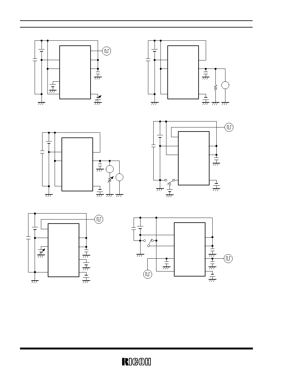
TEST CIRCUITS
OSCILLOSCOPE
E
XT1
GND
C1
C2
D
TC1
V
FB1
V
IN
Vrefout
D
TC2
V
FB2
OSCILLOSCOPE
GND
C1
C2
D
TC1
V
FB1
E
XT2
V
IN
Vrefout
D
TC2
V
FB2
Test Circuit 1
Test Circuit 2
OSCILLOSCOPE
E
XT1
GND
C1
C2
D
TC1
V
FB1
V
IN
Vrefout
D
TC2
V
FB2
OSCILLOSCOPE
GND
C1
D
TC1
V
FB1
E
XT2
V
IN
Vrefout
C2
D
TC2
V
FB2
Test Circuit 3
Test Circuit 4
GND
C1
C2
D
TC1
V
FB1
V
IN
Vrefout
D
TC2
V
FB2
V
GND
C1
C2
D
TC1
V
FB1
V
IN
Vrefout
D
TC2
V
FB2
V
A
Test Circuit 5
Test Circuit 6
R1280D002x
15
OSCILLOSCOPE
E
XT1
GND
C1
C2
AMPOUT
D
TC1
V
FB1
V
IN
Vrefout
D
TC2
V
FB2
OSCILLOSCOPE
E
XT1
GND
C1
D
TC1
V
FB1
V
IN
Vrefout
C2
D
TC2
V
FB2
Test Circuit 7
Test Circuit 8
GND
C1
AMPOUT
D
TC1
V
FB1
V
IN
Vrefout
C2
D
TC2
V
FB2
A
E
XT1
GND
C1
C3
D
TC1
V
FB1
V
IN
Vrefout
C2
D
TC2
V
FB2
OSCILLOSCOPE
CE
Test Circuit 9
Test Circuit 10
GND
C1
D
TC1
V
FB1
E
XT2
V
IN
Vrefout
C2
C4
D
TC2
V
FB2
OSCILLOSCOPE
CE
E
XT1
GND
C1
V
FB1
V
IN
Vrefout
C2
D
TC2
V
FB2
OSCILLOSCOPE
CE
Test Circuit 11
Test Circuit 12
R1280D002x
16
OSCILLOSCOPE
GND
C1
C2
D
TC1
V
FB1
E
XT2
V
IN
Vrefout
V
FB2
CE
GND
C1
V
FB1
V
IN
Vrefout
V
FB2
C2
V
CE
Test Circuit 13
Test Circuit 14
GND
C1
CE
V
FB1
V
IN
Vrefout
V
FB2
C2
V
A
E
XT1
GND
C1
CE
C2
V
FB1
V
IN
Vrefout
V
FB2
OSCILLOSCOPE
Test Circuit 15
Test Circuit 16
E
XT1
GND
C1
CE
C2
V
FB1
V
IN
Vrefout
D
TC2
V
FB2
OSCILLOSCOPE
GND
C1
C3
CE
D
TC1
V
FB1
V
IN
Vrefout
D
TC2
V
FB2
C2
C4
OSCILLOSCOPE
OSCILLOSCOPE
Test Circuit 17
Test Circuit 18

R1280D002x
17
Typical Characteristics shown in the following pages are obtained with test circuits shown above.
∑ R1280D002A/C
Test Circuit 1,2 :
Typical Characteristic 4)
Test Circuit 3 :
Typical Characteristic 6)
Test Circuit 4 :
Typical Characteristic 7)
Test Circuit 5 :
Typical Characteristic 8)
Test Circuit 6 :
Typical Characteristics 9) 10)
Test Circuit 7 :
Typical Characteristic 11)
Test Circuit 8 :
Typical Characteristic 12)
Test Circuit 9 :
Typical Characteristics 13) 14)
∑ R1280D002B
Test Circuit 10,11 :
Typical Characteristics 4) 5)
Test Circuit 12 :
Typical Characteristic 6)
Test Circuit 13 :
Typical Characteristic 7)
Test Circuit 14 :
Typical Characteristic 8)
Test Circuit 15 :
Typical Characteristics 9) 10)
Test Circuit 16 :
Typical Characteristic 11)
Test Circuit 17 :
Typical Characteristics 15) 16)
Test Circuit 18 :
Typical Characteristics 17) 18)
Standard Circuit Example: Typical Characteristics 1) 2) 3) 19) 20)
Note) Capacitors' values of test circuits
Capacitors: Ceramic Type:
C1=4.7µF, C2=1.0µF, C3=C4=1000pF
Efficiency (%) can be calculated with the next formula:
=(V
OUT1
◊I
OUT1
+V
OUT2
◊I
OUT2
)/(V
IN
◊I
IN
)◊100
R1280D002x
18
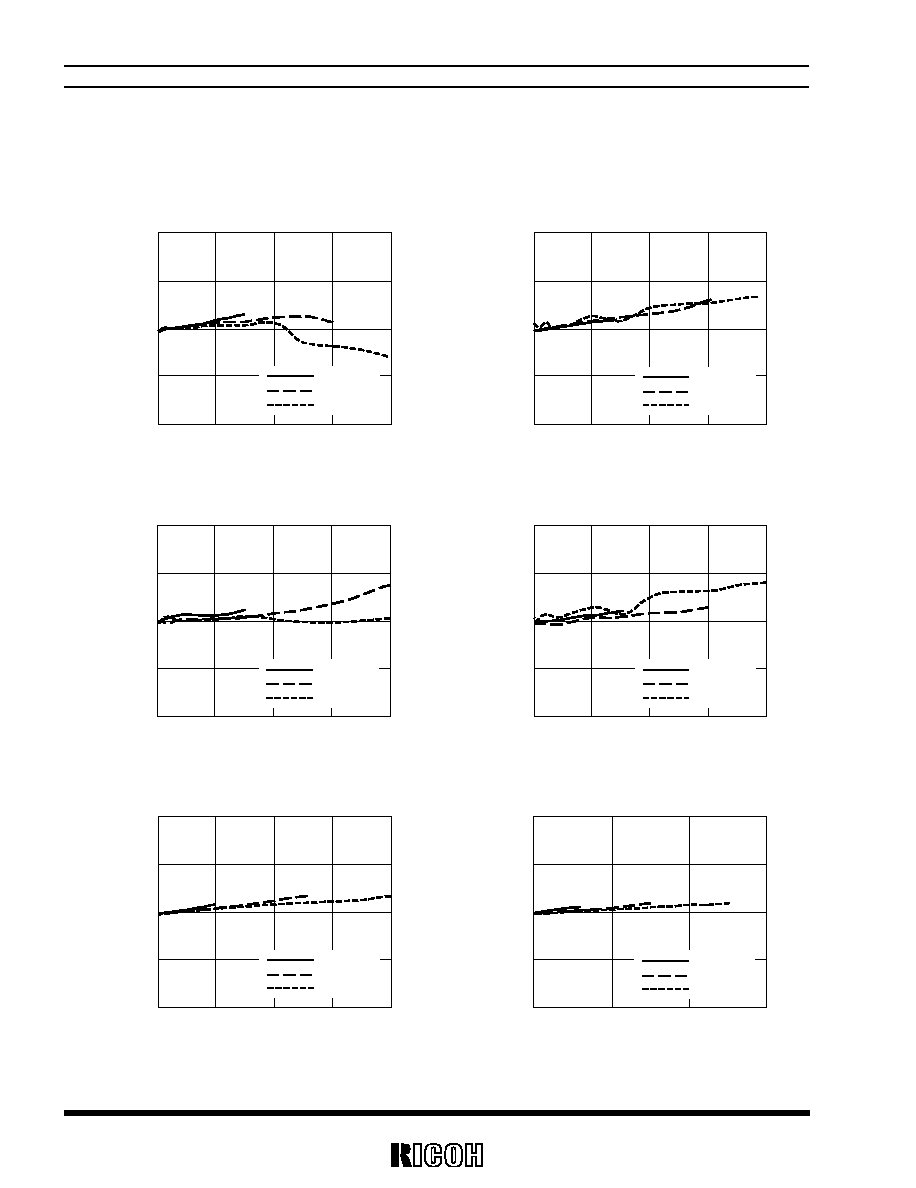
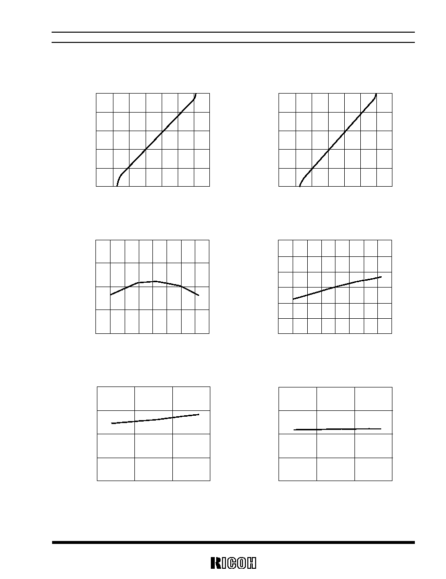
TYPICAL CHARACTERISTICS
1)
Output Voltage vs. Output Current
R1280D002A
R1280D002A
10.10
10.05
10.00
9.95
9.90
Output Current I
OUT1
(mA)
Output Voltage V
OUT1
(V)
0
50
100
150
200
Topt=25
∞C, L1=6.8µH, C1=10µF
V
OUT2
=-10V, I
OUT2
=0mA
V
IN
=2.5V
V
IN
=3.3V
V
IN
=5.5V
-9.90
-9.95
-10.00
-10.05
-10.10
Output Current I
OUT2
(mA)
Output Voltage V
OUT2
(V)
0
-50
-100
-150
-200
Topt=25
∞C, L2=6.8µH, C2=10µF
V
OUT1
=10V, I
OUT1
=0mA
V
IN
=2.5V
V
IN
=3.3V
V
IN
=5.5V
R1280D002B
R1280D002B
10.10
10.05
10.00
9.95
9.90
Output Current I
OUT1
(mA)
Output Voltage V
OUT1
(V)
0
50
100
150
200
Topt=25
∞C, L1=6.8µH, C1=10µF
V
OUT2
=-10V, I
OUT2
=0mA
V
IN
=2.5V
V
IN
=3.3V
V
IN
=5.5V
-9.90
-9.95
-10.00
-10.05
-10.10
Output Current I
OUT2
(mA)
Output Voltage V
OUT2
(V)
0
-50
-100
-150
-200
Topt=25
∞C, L2=6.8µH, C2=10µF
V
OUT1
=10V, I
OUT1
=0mA
V
IN
=2.5V
V
IN
=3.3V
V
IN
=5.5V
R1280D002C
R1280D002C
10.10
10.05
10.00
9.95
9.90
Output Current I
OUT1
(mA)
Output Voltage V
OUT1
(V)
0
50
100
150
200
L1=22
µH, C1=10µF
V
OUT2
=-10V, I
OUT2
=0mA
V
IN
=2.5V
V
IN
=3.3V
V
IN
=5.5V
-9.90
-9.95
-10.00
-10.05
-10.10
Output Current I
OUT2
(mA)
Output Voltage V
OUT2
(V)
0
-50
-100
-150
L2=22
µH, C2=10µF
V
OUT1
=10V, I
OUT1
=0mA
V
IN
=2.5V
V
IN
=3.3V
V
IN
=5.5V
R1280D002x
19
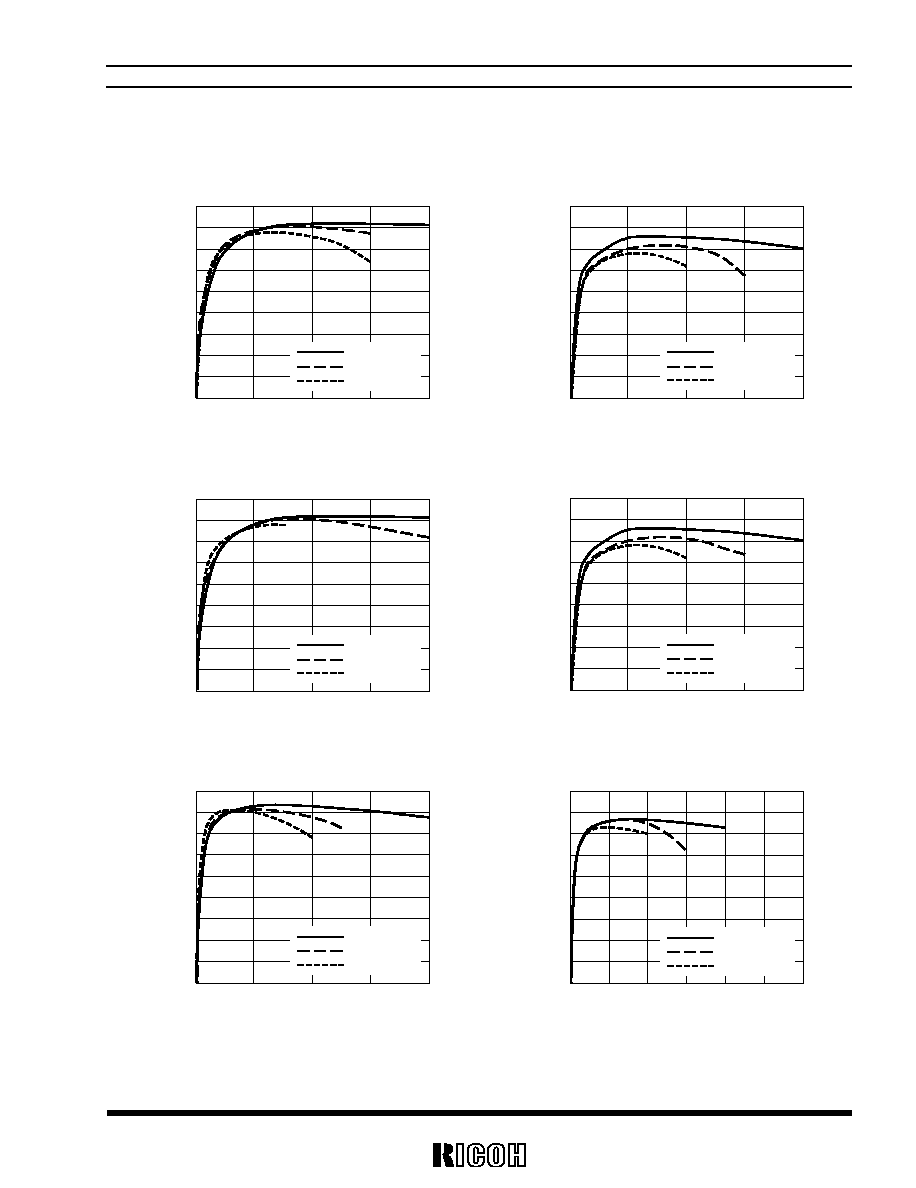
2)
Efficiency vs. Output Current
R1280D002A
R1280D002A
90
80
70
60
50
40
30
20
10
0
Output Current I
OUT1
(mA)
Efficiency
(%)
0
50
100
150
200
V
IN
=3.3V, Topt=25
∞
C, L1=6.8
µH
C1=10
µF, V
OUT2
=-V
OUT1
, I
OUT2
=0mA
V
OUT1
=5V
V
OUT1
=10V
V
OUT1
=15V
90
80
70
60
50
40
30
20
10
0
Output Current I
OUT2
(mA)
Efficiency
(%)
0
-50
-100
-150
-200
V
IN
=3.3V, Topt=25
∞
C, L2=6.8
µH
C2=10
µF, V
OUT1
=-V
OUT2
, I
OUT1
=0mA
V
OUT2
=-5V
V
OUT2
=-10V
V
OUT2
=-15V
R1280D002B
R1280D002B
90
80
70
60
50
40
30
20
10
0
Output Current I
OUT1
(mA)
Efficiency
(%)
0
50
100
150
200
V
IN
=3.3V, Topt=25
∞
C, L1=6.8
µH
C1=10
µF, V
OUT2
=-V
OUT1
, I
OUT2
=0mA
V
OUT1
=5V
V
OUT1
=10V
V
OUT1
=15V
90
80
70
60
50
40
30
20
10
0
Output Current I
OUT2
(mA)
Efficiency
(%)
0
-50
-100
-150
-200
V
IN
=3.3V, Topt=25
∞
C, L2=6.8
µH
C2=10
µF, V
OUT1
=-V
OUT2
, I
OUT1
=0mA
V
OUT2
=-5V
V
OUT2
=-10V
V
OUT2
=-15V
R1280D002C
R1280D002C
90
80
70
60
50
40
30
20
10
0
Output Current I
OUT1
(mA)
Efficiency
(%)
0
50
100
150
200
V
IN
=3.3V, Topt=25
∞
C, L1=22
µH
C1=10
µF, V
OUT2
=-V
OUT1
, I
OUT2
=0mA
V
OUT1
=5V
V
OUT1
=10V
V
OUT1
=15V
90
80
70
60
50
40
30
20
10
0
Output Current I
OUT2
(mA)
Efficiency
(%)
0
-25
-75
-100
-150
-50
-125
V
IN
=3.3V, Topt=25
∞
C, L2=22
µH
C2=10
µF, V
OUT1
=-V
OUT2
, I
OUT1
=0mA
V
OUT2
=-5V
V
OUT2
=-10V
V
OUT2
=-15V

R1280D002x
20
3)
Output Voltage vs. Temperature
R1280D002A
R1280D002A
11.0
10.5
9.5
9.0
Temperature Topt(
∞C)
Output Voltage V
OUT1
(V)
-60 -40
20
60
100
-20
40
0
80
10.0
V
IN
=3.3V, L1=6.8
µH, C1=10µF
I
OUT
=10mA
I
OUT
=100mA
-9.0
-9.5
-10.5
-11.0
Temperature Topt(
∞C)
Output Voltage V
OUT2
(V)
-60 -40
20
60
100
-20
40
0
80
-10.0
V
IN
=3.3V, L2=6.8
µH, C2=10µF
I
OUT
=-10mA
R1280D002B
R1280D002B
11.0
10.5
9.5
9.0
Temperature Topt(
∞C)
Output Voltage V
OUT1
(V)
-60 -40
20
60
100
-20
40
0
80
10.0
V
IN
=3.3V, L1=6.8
µH, C1=10µF
I
OUT
=10mA
I
OUT
=100mA
-9.0
-9.5
-10.5
-11.0
Temperature Topt(
∞C)
Output Voltage V
OUT2
(V)
-60 -40
20
60
100
-20
40
0
80
-10.0
V
IN
=3.3V, L2=6.8
µH, C2=10µF
I
OUT
=-10mA
R1280D002C
R1280D002C
11.0
10.5
9.5
9.0
Temperature Topt(
∞C)
Output Voltage V
OUT1
(V)
-60 -40
20
60
100
-20
40
0
80
10.0
V
IN
=3.3V, L1=22
µH, C1=10µF
I
OUT
=10mA
I
OUT
=100mA
-9.0
-9.5
-10.5
-11.0
Temperature Topt(
∞C)
Output Voltage V
OUT2
(V)
-60 -40
20
60
100
-20
40
0
80
-10.0
V
IN
=3.3V, L2=22
µH, C2=10µF
I
OUT
=-10mA

R1280D002x
21
4)
Frequency vs. Temperature
R1280D002A
R1280D002B
800
750
600
550
Temperature Topt(
∞C)
Frequency fosc(kHz)
-60
-20
20
60
100
-40
0
40
80
700
650
V
IN
=2.5V
V
IN
=3.3V
V
IN
=5.5V
800
750
600
550
Temperature Topt(
∞C)
Frequency fosc(kHz)
-60
-20
20
60
100
-40
0
40
80
700
650
V
IN
=2.5V
V
IN
=3.3V
V
IN
=5.5V
R1280D002C
230
210
150
Temperature Topt(
∞C)
Frequency fosc(kHz)
-60
-20
20
60
100
-40
0
40
80
190
170
V
IN
=2.5V
V
IN
=3.3V
V
IN
=5.5V
5)
Maximum Duty Cycle vs. Temperature
R1280D002B
R1280D002B
94
92
86
Temperature Topt(
∞C)
-60
-20
20
60
100
-40
0
40
80
90
88
Maximum Duty Cycle
maxduty1(%)
V
IN
=3.3V
94
92
86
Temperature Topt(
∞C)
-60
-20
20
60
100
-40
0
40
80
90
88
Maximum Duty Cycle
maxduty2(%)
V
IN
=3.3V
R1280D002x
22
6)
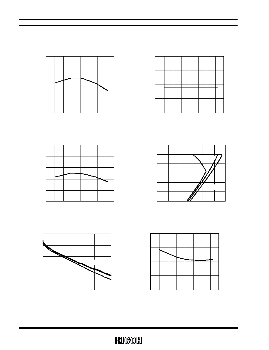
Feedback Voltage vs. Temperature
7)
Input Offset Voltage vs. Temperature
R1280D002A/B/C
R1280D002A/B/C
1.02
1.01
0.97
Temperature Topt(
∞C)
-60
-20
20
60
100
-40
0
40
80
1.00
0.99
0.98
Feedback Voltage V
FB1
(V)
V
IN
=3.3V
10.0
5.0
-10.0
Temperature Topt(
∞C)
-60
-20
20
60
100
-40
0
40
80
0.0
-5.0
Input Offset Voltage V
FB2
(mV)
V
IN
=3.3V
8)
Vrefout Output Voltage vs. Temperature
9)
Vrefout Output Voltage vs. Output Current
R1280D002A/B/C
R1280D002A/B/C
1.55
1.53
1.45
Temperature Topt(
∞C)
-60
-20
20
60
100
-40
0
40
80
1.51
1.49
1.47
Vrefout Voltage (V)
V
IN
=3.3V
1.8
1.5
0
I
ROUT
(mA)
0
20
30
50
60
10
40
1.2
0.9
0.6
0.3
Vrefout Voltage (V)
V
IN
=5.5V
V
IN
=2.5V
V
IN
=3.3V
10) Vrefout Output Voltage vs. Output Current
11) Protection Circuit Delay Time vs. Temperature
R1280D002A/B/C
R1280D002A/B/C
1.508
1.506
1.498
I
ROUT
(mA)
0
10
15
20
5
1.504
1.502
1.500
Vrefout Voltage (V)
V
IN
=5.5V
V
IN
=2.5V
V
IN
=3.3V
140
120
60
Temperature Topt(
∞C)
-60
-20
20
60
100
-40
0
40
80
100
80
Protection Circuit Delay Time
T
DLY
(msec)
V
IN
=3.3V
R1280D002x
23
12) Duty Cycle vs. DTC Voltage
R1280D002A
R1280D002C
100
80
0
V
DTC
(V)
0
1.4
0.2
0.4
0.6
0.8
1
1.2
60
40
20
Duty Cycle Duty(%)
V
IN
=3.3V, EXT=1000pF
100
80
0
V
DTC
(V)
0
1.4
0.2
0.4
0.6
0.8
1
1.2
60
40
20
Duty Cycle Duty(%)
V
IN
=3.3V, EXT=1000pF
13) Output Sink Current vs. Temperature
14) Output Source Current vs. Temperature
R1280D002A/C
R1280D002A/C
130
120
90
Temperature Topt(
∞C)
-60
-20
20
60
100
-40
0
40
80
110
100
Output Sink Current I
AMPL
(
µ
A)
V
IN
=3.3V
0.0
-0.5
-3.0
Temperature Topt(
∞C)
-60
-20
20
60
100
-40
0
40
80
-1.5
-1.0
-2.0
-2.5
Output Sink Current I
AMPH
(mA)
V
IN
=3.3V
15) CE "H" Input Voltage vs. Temperature
16) CE "L" Input Voltage vs. Temperature
R1280D002B
R1280D002B
1.25
0.25
Temperature Topt(
∞C)
-50
50
100
0
0.75
1.00
0.50
CEH Input Voltage V
CEH
(V)
V
IN
=5.5V
1.25
0.25
Temperature Topt(
∞C)
0.75
1.00
0.50
CE
L
Input Voltage V
CEL
(V)
V
IN
=2.5V
-50
50
100
0

R1280D002x
24
17) Soft Starting Time vs. Capacitance value
R1280D002B
R1280D002B
40
0
Capacitance Value for Soft Start (
µF)
0
0.4
0.8
1.2
0.2
0.6
1
20
30
10
Soft Starting Time T
SS1
(ms)
V
IN
=3.3V
50
0
Capacitance value for Soft Start (
µF)
0
0.4
0.8
1.2
0.2
0.6
1
20
30
40
10
Soft Starting Time T
SS2
(ms)
V
IN
=3.3V
18) Soft Starting Time vs. Temperature
R1280D002B
R1280D002B
20
0
Temperature Topt(
∞C)
10
15
5
Soft Starting Time T
SS1
(ms)
V
IN
=3.3V, C
DTC1
=0.33
µF
-50
50
100
0
30
0
Temperature Topt(
∞C)
10
25
20
15
5
Soft Starting Time T
SS2
(ms)
V
IN
=3.3V, C
DTC2
=0.33
µF
-50
50
100
0
19) Load Transient Response(Step-up Side)
R1280D002A
R1280D002A
10.5
7.5
Time (s)
0
0.002
0.0005
0.001
0.0015
8.5
10
9.5
9
8
Output Voltage V
OUT1
(V)
Output Current I
OUT
(mA)
V
IN
=3.3V, L1=6.8
µH
0.1
100
11.5
8.5
Time (s)
0
0.05
0.01
0.02
0.03
0.04
9.5
11
10.5
10
9
Output Voltage V
OUT1
(V)
Output Current I
OUT
(mA)
V
IN
=3.3V, L1=6.8
µH
0.1
100

R1280D002x
25
R1280D002B
R1280D002B
10.5
7.5
Time (s)
0
0.002
0.0005
0.001
0.0015
8.5
10
9.5
9
8
Output Voltage V
OUT1
(V)
Output Current I
OUT
(mA)
V
IN
=3.3V, L1=6.8
µH
0.1
100
11.5
8.5
Time (s)
0
0.05
0.01
0.02
0.03
0.04
9.5
11
10.5
10
9
Output Voltage V
OUT1
(V)
Output Current I
OUT
(mA)
V
IN
=3.3V, L1=6.8
µH
0.1
100
R1280D002C
R1280D002C
10.5
7.5
Time (s)
0
0.002
0.0005
0.001
0.0015
8.5
10
9.5
9
8
Output Voltage V
OUT1
(V)
Output Current I
OUT
(mA)
V
IN
=3.3V, L1=22
µH
0.1
100
11.5
8.5
Time (s)
0
0.05
0.01
0.02
0.03
0.04
9.5
11
10.5
10
9
Output Voltage V
OUT1
(V)
Output Current I
OUT
(mA)
V
IN
=3.3V, L1=22
µH
0.1
100
20) Load Transient Response (Inverting Side)
R1280D002A
R1280D002A
-9
-11.5
Time (s)
0.0006
0.0001 0.0002 0.0003 0.0004 0.0005
-11
-10.5
-10
-9.5
Output Voltage V
OUT2
(V)
Output Current I
OUT
(mA)
V
IN
=3.3V, L2=6.8
µH
-0.1
-50
0.0000
-9.5
-12
Time (s)
0.000
0.020
0.005
0.010
0.015
-11
-10
-10.5
-11.5
Output Voltage V
OUT2
(V)
Output Current I
OUT
(mA)
V
IN
=3.3V, L2=6.8
µH
-0.1
-50

R1280D002x
26
R1280D002B
R1280D002B
-9
-11.5
Time (s)
-11
-10.5
-10
-9.5
Output Voltage V
OUT2
(V)
Output Current I
OUT
(mA)
V
IN
=3.3V, L2=6.8
µH
-0.1
-50
0.0006
0.0001 0.0002 0.0003 0.0004 0.0005
0.0000
-9.5
-12
Time (s)
0.000
0.020
0.005
0.010
0.015
-11
-10
-10.5
-11.5
Output Voltage V
OUT2
(V)
Output Current I
OUT
(mA)
V
IN
=3.3V, L2=6.8
µH
-0.1
-50
R1280D002C
R1280D002C
-9
-11.5
Time (s)
-11
-10.5
-10
-9.5
Output Voltage V
OUT2
(V)
Output Current I
OUT
(mA)
V
IN
=3.3V, L2=22
µH
-0.1
-50
0.0006
0.0001 0.0002 0.0003 0.0004 0.0005
0.0000
-9.5
-12
Time (s)
0.000
0.020
0.005
0.010
0.015
-11
-10
-10.5
-11.5
Output Voltage V
OUT2
(V)
Output Current I
OUT
(mA)
V
IN
=3.3V, L2=22
µH
-0.1
-50

R1280D002x
27
TYPICAL APPLICATION AND TECHNICAL NOTES
∑ R1280D002A/C
External Components
Inductor L1,2: 6.8
µH, LDR655312T (TDK) for A type, 22µH for C type
Diode:
FS1J3 (Origin Electronics)
NMOS:
IRF7601 (International Rectifier)
PMOS:
Si3443DV (Siliconix)
Resistors:
R1, R2, R3, and R4 are for Setting Output Voltage. Recommendation values are
R1+R2
100k or R3+R4100k
R5=43k
, R6=10k, R7=R9=22k, R8=R10=43k, R11=220k
Capacitors:
Ceramic Capacitor
(Example)
R1280D002A:
C1=C2=10
µF, C3=4.7µF, C4=0.22µF, C5=0.47µF, C6=120pF, C7=50pF,
C8=1
µF, C9=1000pF
R1280D002C: C1=C2=10
µF, C3=4.7µF, C4=0.22µF, C5=0.47µF, C6=220pF, C7=330pF,
C8=1
µF, C9=1000pF
Note: Maximum voltage tolerance of each component should be considered. With the transistor
shown above is appropriate to set up to
±15V as output voltage.
E
XT1
GND
C3
NMOS
V
OUT1
V
OUT2
L1
D
TC1
V
FB1
E
XT2
V
IN
D
TC2
V
FB2
AMPOUT1
Vrefout
C5
R10
R9
C8
R4
R6
R3
R5
C6
R2
R1
C1
Diode
PMOS
C7
C2
L2
C4
C9
R11
R8
R7
R1280D002x
28
∑ R1280D002B
E
XT1
GND
C3
NMOS
V
OUT1
V
OUT2
L1
D
TC1
V
FB1
E
XT2
V
IN
D
TC2
V
FB2
CE
Vrefout
C5
C8
R4
R6
R3
R5
C6
R2
R1
C1
Diode
PMOS
C7
C2
L2
C4
External Components
Inductor L1,2: 6.8
µH, LDR655312T (TDK)
Diode:
FS1J3 (Origin Electronics)
NMOS:
IRF7601 (International Rectifier)
PMOS:
Si3443DV (Siliconix)
Resistors:
R1, R2, R3, and R4 are for Setting Output Voltage. Recommendation values are
R1+R2
100k or R3+R4100k
R5=43k
, R6=10k
Capacitors:
Ceramic Capacitor
(Example)
C1=C2=10
µF, C3=4.7µF, C4=0.33µF, C5=0.33µF, C6=120pF, C7=50pF, C8=1µF
Note: Maximum voltage tolerance of each component should be considered. With the transistor
shown above is appropriate to set up to
±15V as output voltage.
R1280D002x
29
APPLICATION EXAMPLE
∑ R1280D002A/C
E
XT1
GND
C3
NMOS
V
OUT1
V
OUT2
L1
D
TC1
V
FB1
E
XT2
V
IN
D
TC2
V
FB2
AMPOUT1
Vrefout
C5
R10
R9
C8
R4
R6
R3
R5
C6
R2
R1
C1
Diode
PMOS
C7
C2
L2
C4
C9
R11
R8
R7
C11
C10
V
OUT3
External Components
Inductor L1,2: 6.8
µH, LDR655312T (TDK) for A version, 22µH for R1280D002C
Diode:
FS1J3 (Origin Electronics)
NMOS:
IRF7601 (International Rectifier)
PMOS:
Si3443DV (Siliconix)
Resistors:
R1, R2, R3, and R4 are for Setting Output Voltage. Recommendation values are
R1+R2
100k or R3+R4100k
R5=43k
, R6=10k, R7=R9=22k, R8=R10=43k, R11=220k
Capacitors:
Ceramic Capacitor
(Example)
R1280D002A:
C1=C2=10
µF, C3=4.7µF, C4=0.22µF, C5=0.47µF, C6=120pF, C7=50pF,
C8=C10=C11=1
µF, C9=1000pF
R1280D002C: C1=C2=10
µF, C3=4.7µF, C4=0.22µF, C5=0.47µF, C6=220pF, C7=330pF,
C8=C10=C11=1
µF, C9=1000pF
This IC can be used 3 Output TFT Bias Circuit as shown above. V
OUT3
=2xV
OUT1
-Vf
Note: Maximum voltage tolerance of each component should be considered. With the transistor
shown above is appropriate to set up to +15V as V
OUT1
, -15V as V
OUT2
, 30V as V
OUT3
.
R1280D002x
30
∑ R1280D002B
E
XT1
GND
C3
NMOS
V
OUT1
V
OUT2
L1
D
TC1
V
FB1
E
XT2
V
IN
D
TC2
V
FB2
CE
Vrefout
C5
C8
R4
R6
R3
R5
C6
R2
R1
C1
Diode
PMOS
C7
L2
C4
L1
C11
C10
V
OUT3
External Components
Inductor L1,2: 6.8
µH, LDR655312T (TDK)
Diode:
FS1J3 (Origin Electronics)
NMOS:
IRF7601 (International Rectifier)
PMOS:
Si3443DV (Siliconix)
Resistors:
R1, R2, R3, and R4 are for Setting Output Voltage. Recommendation values are
R1+R2
100k or R3+R4100k, R5=43k, R6=10k,
Capacitors:
Ceramic Capacitor
(Example)
R1280D002B:
C1=C2=10
µF, C3=4.7µF, C4=0.22µF, C5=0.33µF, C6=120pF, C7=50pF,
C8=C10=C11=1
µF
This IC can be used 3 Output TFT Bias Circuit as shown above. V
OUT3
=2xV
OUT1
-Vf
Note: Maximum voltage tolerance of each component should be considered. The transistor shown
above is appropriate to set up to +15V as V
OUT1
, -15V as V
OUT2
, 30V as V
OUT3

R1280D002x
31
EXTERNAL COMPONENTS
1.
How to set the output voltages
As for step-up side, feedback (V
FB1
) pin voltage is controlled to maintain 1V, therefore,
V
OUT1
: R1+R2=V
FB1
: R2
Thus, V
OUT1
=V
FB1
◊(R1+R2)/R2
Output Voltage is adjustable with R1 and R2.
As for inverting side, Feedback (V
FB2
) pin voltage is controlled to maintain 0V, therefore,
Vrefout : R3=|-V
OUT2
|:R4
Thus, |-V
OUT2
|=Vrefout◊R4/R3
Output Voltage is adjustable with R3 and R4.
2.
How to set Soft-Start Time
As for R1280D002B, soft-start time is adjustable with connecting a capacitor to DTC pin.
Soft starting time, T
SS1
and T
SS2
are adjustable. Soft-start time can be set with the time constant of RC.
Soft-start time can be described as in next formula. (Topt=25∞C)
T
SS1
RS1◊C4, T
SS2
RS2◊C5
In the above formulas, RS1 value is Typ. 32k, while RS2 value is Typ. 45k. Tolerance of these values is ±25%
caused by dispersion of wafer process parameters.
On the other hand, as for R1280D002A/C, each soft-start time is set with the time constant of each external resistors
and capacitor shown as in the next formula.
T
SS1
R
O1
◊C4, T
SS2
R
O2
◊C5
In the above formula, R
O1
=(R7◊R8)/(R7+R8), R
O2
=(R9◊R10)/(R9+R10)

R1280D002x
32
TECHNICAL NOTES on EXTERNAL COMPONENTS
∑ External components should be set as close to this IC as possible. Especially, wiring of the capacitor connected to
V
IN
pin should be as short as possible.
∑ Enforce the ground wire. Large current caused by switching operation flows through GND pin. If the impedance of
ground wire is high, internal voltage level of this IC might fluctuate and operation could be unstable.
∑ Recommended capacitance value of C3 is equal or more than 4.7µF. Recommended maximum voltage tolerance of
C3 is three times as large as set output voltage or more, because the external transistor might generate a high volt-
age with a shape of spike because of an effect from inductor.
∑ If the spike noise of V
OUT
is too large, the noise is feedback from V
FB1
pin and operation might be unstable. In that
case, use the resistor ranging from 10k to 50k as R5 and try to reduce the noise level. In the case of V
OUT2
, use
the resistor as much as 10k as R6.
∑ Select an inductor with low D.C. current, large permissible current, and uneasy to cause magnetic saturation. If the
inductance value is too small, IL
X
might be beyond the absolute maximum rating at the maximum load.
∑ Select a Schottky diode with fast switching speed and large enough permissible current.
∑ Recommended capacitance value of C1 and C2 is as much as Ceramic 10µF. In case that the operation with the sys-
tem of DC/DC converter would be unstable, add a series resister less than 0.5 to each output capacitor or use
tantalum capacitors with appropriate ESR. If you choose too large ESR, ripple noise may be forced to V
FB1
and V
FB2
,
and unstable operation may result. Use a capacitor with three times as large as voltage tolerance of the capacitor.
∑ In this IC, for the test efficiency, Latch release function is included. By forcing (V
IN
-0.3)V or more voltage to DTC1
pin or DTC2 pin, Latch release function works.
∑ Consider the threshold voltage of Power MOSFET transistor. Select an appropriate MOSFET transistor, depending
on the input voltage in order to make the MOSFET turn on completely.
∑ Performance of the power controller with using this IC depends on external components. Each component, layout
should not be beyond each absolute maximum rating such as voltage, current, and power dissipation.