
LOW VOLTAGE DETECTOR
R3111xxxxA/C SERIES
1
OUTLINE
The R3111 series are CMOS-based voltage detector ICs with high detector threshold accuracy and
ultra-low supply current, which can be operated at an extremely low voltage and is used for system
reset as an example.
Each of these ICs consists of a voltage reference unit, a comparator, resistors for detector threshold
setting, an output driver and a hysteresis circuit. The detector threshold is fixed with high accuracy
internally and does not require any adjustment.
Two output types, Nch open drain type and CMOS type are available.
The R3111 Series are operable at a lower voltage than that for the RX5VL series, and can be driven
by a single battery.
Six types of packages, TO-92, SOT-89, SOT-23-3, SOT-23-5, SC-82AB, and SON1612-6(Under
Development) are available.
FEATURES
∑
Ultra-low Supply Current .........................................Typ. 0.8µA (V
DD
=1.5V)
∑
Wide Range of Operating Voltage ..............................0.7V to 10.0V (Topt=25
∞
C)
∑
Detector Threshold...................................................Stepwise setting with a step of 0.1V in the
range of 0.9V to 6.0V is possible.
∑
High Accuracy Detector Threshold............................±2.0%
∑
Low Temperature-Drift Coefficient of Detector Threshold Typ. ±100ppm/
∞
C
∑
Two Output Types....................................................Nch Open Drain and CMOS
∑
Four Types of Packages ............................................TO-92, SOT-89(Mini-power Mold), SOT-23-3,
SOT-23-5 (Mini-mold), SC-82AB,
SON1612-6(Under development)
APPLICATIONS
∑
CPU and Logic Circuit Reset
∑
Battery Checker
∑
Window Comparator
∑
Wave Shaping Circuit
∑
Battery Back-up Circuit
∑
Power Failure Detector

R3111xxxxA/C
2
BLOCK DIAGRAMS
R3111xxxxA
R3111xxxxC
V
DD
OUT
GND
Vref
V
DD
OUT
GND
Vref
TIMING CHART
t
PLH
Supply Voltage
Output Voltage
(OUT)
Minimum Operating Voltage
V
SS
V
SS
Detector Threshold
Hysteresis
(V
DD
)
Release Voltage +V
DET
Detector Threshold -V
DET
DEFINITION OF OUTPUT DELAY TIME
Output Delay Time t
PLH
is defined as follows:
1. In the case of Nch Open Drain Output:
Under the condition of the output pin (OUT) is pulled up through a resistor of 470k
to 5V, the
time interval between the rising edge of V
DD
pulse from 0.7V to (+V
DET
)+ 2.0V and becoming of the
output voltage to 2.5V.
2. In the case of CMOS Output:
The time interval between the rising edge of V
DD
pulse from 0.7V to (+V
DET
)+ 2.0V and becoming of
the output voltage to (V
DD
/
2) V.

R3111xxxxA/C
3
+V
DET
+ 2.0V
5.0V
2.5V
0.7V
Input Voltage
(V
DD
)
Output Voltage
GND
GND
t
PHL
t
PLH
+V
DET
+ 2.0V
+V
DET
+2.0V
+V
DET
+2.0V
0.7V
Input Voltage
(V
DD
)
Output Voltage
GND
2
GND
t
PHL
t
PLH
Nch Open Drain Output
CMOS Output
SELECTION GUIDE
The package type, the detector threshold, the output type and the taping type of R3111 Series can be
designated at the users' request by specifying the part number as follows;
R3111xxxxx-xx
Part Number
a b cd e
Code
Contents
a
Designation of Package Type;
E: TO-92
Q: SC-82AB
H: SOT-89 N: SOT-23-5 / SOT-23-3 D: SON1612-6(Under Development)
b
Setting Detector Threshold (-V
DET
);
Stepwise setting with a step of 0.1V in the range of 0.9V to 6.0V is possible.
c
Designation of Package Type
1: except SOT-23-3
2: SOT-23-3
d
Designation of Output Type;
A: Nch Open Drain
C: CMOS
e
Designation of Packing or Taping Type ;
Ex.TO-92: TZ, SOT-89: T1, SOT-23-3, SOT-23-5, SC-82AB, SON1612-6
Under Development: TR prescribed as standard directions.
(Refer to Taping Specifications.) Antistatic bag for samples: C
R3111xxxxA/C
5
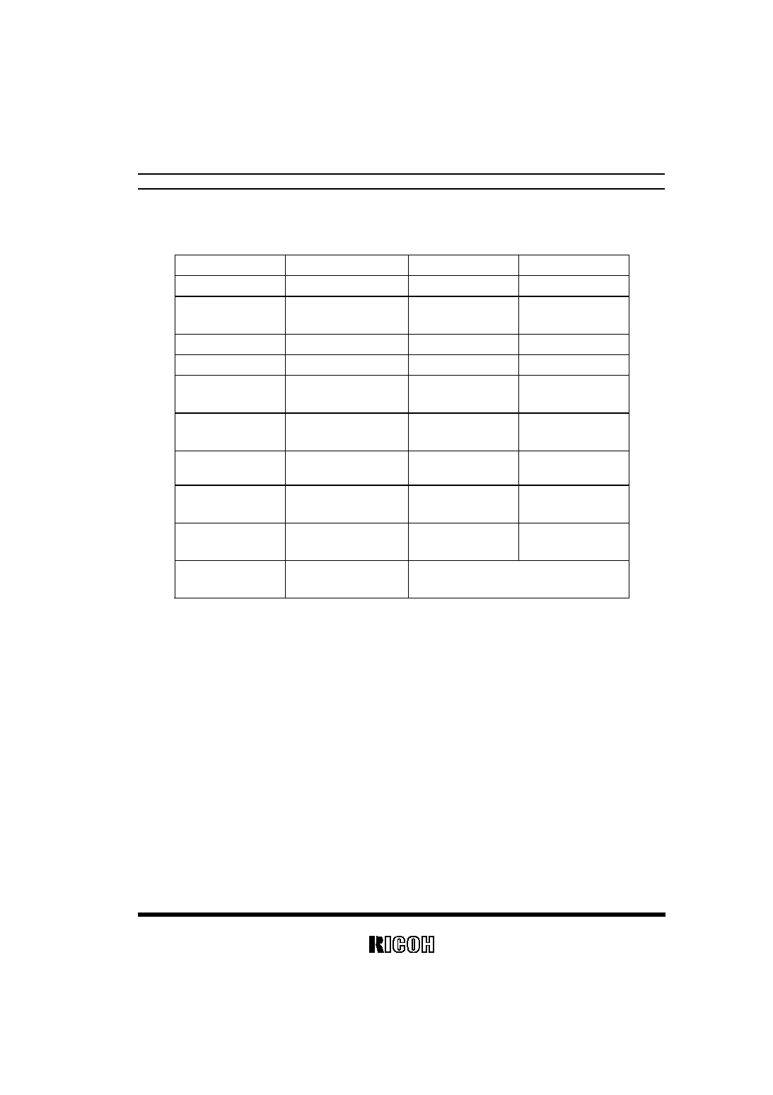
ABSOLUTE MAXIMUM RATINGS
Symbol
Item
Rating
Unit
V
DD
Supply Voltage
12
V
V
OUT1
Output Voltage
(CMOS)
V
SS
-0.3 to V
DD
+0.3
V
V
OUT2
Output Voltage (Nch)
V
SS
-0.3 to 12
V
I
OUT
Output Current
70
mA
P
D
Power Dissipation
1*
Note1
300
mW
P
D
Power Dissipation
2*
Note2
150
mW
P
D
Power Dissipation
3*
Note3
500
mW
Topt
Operating Tempera-
ture Range
-40 to 85
∞
C
Tstg
Storage Temperature
Range
-55 to 125
∞
C
Tsolder
Lead temperature
(Soldering)
260
∞
C, 10s
*Note 1: applied to SOT-89 and TO-92 Single suspended in the air
*Note 2: applied to SOT-23-3, SOT-23-5 and SC-82AB Single suspended in the air
*Note 3: applied to SON1612-6(Under Development) at mounted on board
PD depends on conditions of mounting on board. This specification is based on
the measurement at the condition below:
*Measurement Conditions
Environment: Mounted on board (Wind velocity 0m/s)
Board Material: FR-4 (2-layer)
Board dimensions : 40mm x 40mm x t1.6mm
Copper Area : 50%
