
LOW VOLTAGE DETECTOR WITH OUTPUT
DELAY
R3112xxx1A/C SERIES
1
R3112X_E/2003/10/20
OUTLINE
The R3112 Series are CMOS-based voltage detector ICs with high detector threshold accuracy and
ultra-low supply current, which can be operated at an extremely low voltage and is used for system
reset as an example.
Each of these ICs consists of a voltage reference unit, a comparator, resistor net for detector
threshold setting, an output driver, a hysteresis circuit, and an output delay circuit. The detector
threshold is fixed with high accuracy internally and does not require any adjustment. Two output types,
Nch open drain type and CMOS type are available.
Three types of packages, SOT-23-5, small SC-82AB, and ultra-small SON1612-6(Under Develop-
ment) can be selected so that high density mounting on boards is possible.
FEATURES
∑
Built-in Output Delay Circuit .......................................... Typ. 100ms with an external capacitor:
0.022
µ
F
∑
Ultra-low Supply Current
.................................................................
Typ. 1.0µA (V
DD
=3.5V)
∑
Wide Range of Operating Voltage
...................................................
0.7~6.0V(Topt=25
∞
C)
∑
Detector Threshold
.............................................................................
Stepwise setting with a step of 0.1V in
the range of 0.9V to 5.0V is possible.
∑
High Accuracy Detector Threshold
................................................
±2.0%
∑
Low Temperature-Drift Coefficient of Detector Threshold
.....
Typ. ±100ppm/
∞
C
∑
Two Output Types
...............................................................................
Nch Open Drain and CMOS
∑
Three Types of Packages
...................................................................
SOT-23-5 (Mini-mold), SC-82AB,
SON1612-6(Under Development)
APPLICATIONS
∑
CPU and Logic Circuit Reset
∑
Battery Checker
∑
Window Comparator
∑
Wave Shaping Circuit
∑
Battery Back-up Circuit
∑
Power Failure Detector
R3112xxx1A/C
2
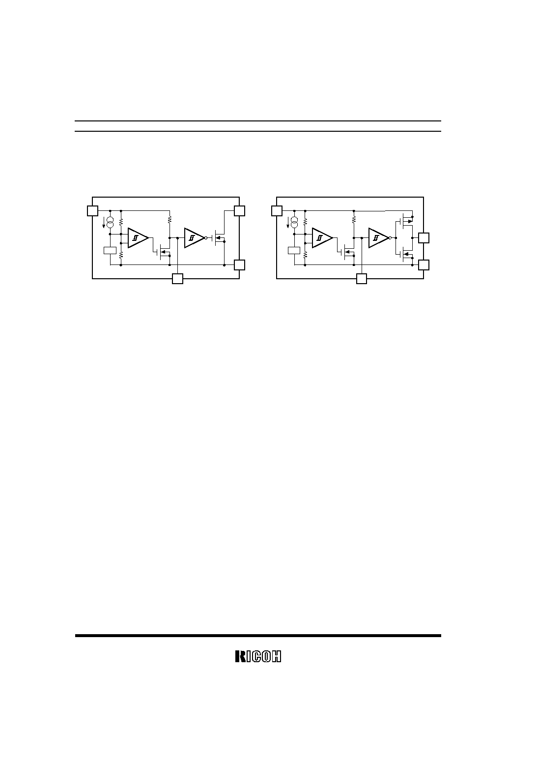
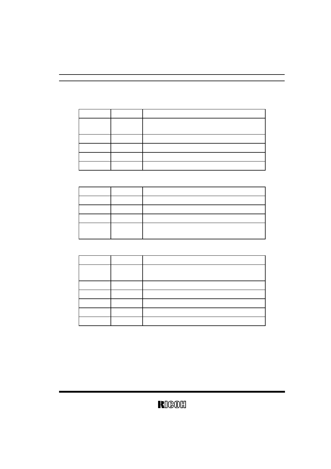
BLOCK DIAGRAMS
R3112xxx1A
R3112xxx1C
GND
V
DD
-
+
Vref
OUT
R
D
C
D
GND
V
DD
-
+
Vref
OUT
R
D
C
D
R3112xxx1A/C
3
OPERATION
V
DD
Pch
Rc
Tr.1
Tr.2
Rb
Ra
Nch
R
D
O
UT
C
D
GND
+
-
Vref
Schmitt Trigger
Comparator
Current Source
Output Capacitor
Fig. 1 Block Diagram with an external capacitor
HYSTERESIS
RANGE
1
GND
GND
Delay Time
A
B
Output Voltage(OUT)
Supply Voltage(V
DD
)
V
DDL
-V
DET
+V
DET
Minimum Operating
Voltge
Detector Threshold
Released Voltage
2
3
4
5
Operation Status
Compartor(-) Pin
Input Voltage
Compartor Output
Tr.1, 2
1
I
I
V
DD
L
OFF
Rb+Rc
Ra+Rb+Rc
OFF
ON
Output Tr.
Nch
Pch
2
II
H
ON
ON
OFF
4
II
H
ON
ON
OFF
5
I
L
OFF
OFF
ON
3
II
Indefinite
Indefinite
Indefinite
Indefinite
+
II
V
DD
Rb
Ra+Rb
+
Fig. 2 Operation Diagram
1. Output voltage is equal to supply voltage. (As for Nch open drain type, equal to pull-up voltage.)
2. When the supply voltage is down to the detector threshold voltage level(Point A),
Vref
V
DD
◊
(
Rb+Rc)/(Ra+Rb+Rc) is true, then output of the comparator is reversed from "L" to "H",
therefore output voltage becomes GND level.
3. When the supply voltage is lower than minimum operating voltage, the operation of output tran-
sistor is indefinite. In the case of Nch open drain type, output voltage is equal to pull-up voltage.
4. Output Voltage becomes GND level.
5. When the supply voltage is higher than released voltage (Point B), Vref
V
DD
◊
Rb/(Ra+Rb) is true, then

R3112xxx1A/C
4
output of the comparator reaches the threshold level, and Output of Shmitt Trigger is reversed from
"H" to "L", then output voltage is equal to supply voltage. (As for Nch open drain type, equal to
pull-up voltage.)
*) The difference between released voltage and detector threshold voltage means hysteresis range
voltage.
R3112xxx1A/C
5
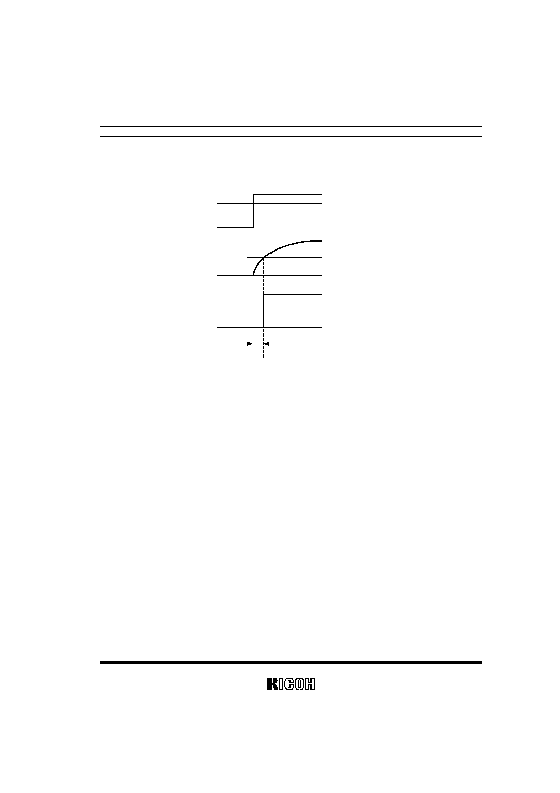
∑
Operation of Output Delay
GND
GND
Released Voltage (+V
DET
)
C
D
Pin Threshold Voltage (V
TCD
)
Output Delay Time(t
D
)
Output Voltage
Capacitor Voltage
Supply Voltage
When the supply voltage which is higher than released voltage is forced to V
DD
pin, charge to an
external capacitor starts, then capacitor voltage increases. Until the capacitor voltage reaches to C
D
Pin
threshold voltage, output voltage maintains "L". When the capacitor voltage becomes higher than C
D
pin threshold voltage, output voltage is reversed from "L" to "H". Where, the time interval between the
rising edge of supply voltage and output voltage reverse point means output delay time.
∑
Output Delay Time
Output Delay Time (t
D
) can be calculated with the next formula.
t
D
=0.69
◊
R
D
◊
C
D
(s)
R
D
is internal resistor and set at 6.5M
(Typ.) typically. C
D
(F) describes the capacitance value of an
external capacitor. Therefore,
t
D
=0.69
◊
6.5
◊
10
6
◊
C
D
(s)
R3112xxx1A/C
6
SELECTION GUIDE
The package type, the detector threshold, the output type, and the taping type of R3112 Series can
be designated at the users' request by specifying the part number as follows;
R3112xxx1x-xx
Part Number
a
b
c
d
Code
Contents
a
Designation of Package Type;
Q:SC-82AB
N:SOT-23-5 D:SON1612-6(Under Development)
b
Setting Detector Threshold (-V
DET
);
Stepwise setting with a step of 0.1V in the range of 0.9V to 5.0V is possible.
c
Designation of Output Type;
A: Nch Open Drain
C: CMOS
d
Designation of Packing or Taping Type ;
Ex. SOT-23-5, SC-82AB, SON1612-6(Under Development): TR is prescribed
as standard directions.
(Refer to Taping Specifications)
PIN CONFIGURATION
SOT-23-5
SC82-AB
SON1612-6(Under Development)
1
2
3
5
4
(mark side)
4
3
1
2
(mark side)
6 5 4
1 2 3
R3112xxx1A/C
7
PIN DESCRIPTION
SOT-23-5
Pin No.
Symbol
Description
1
OUT
Output Pin(Output "L" at detector threshold, Output
"H" at released voltage)
2
V
DD
Voltage Supply Pin
3
GND
Ground Pin
4
NC
No Connection
5
C
D
Pin for External Capacitor (for setting output delay)
SC-82AB
Pin No.
Symbol
Description
1
V
DD
Voltage Supply Pin
2
GND
Ground Pin
3
C
D
Pin for External Capacitor (for setting output delay)
4
OUT
Output Pin(Output "L" at detector threshold, Output
"H" at released voltage)
SON1612-6(Under Development)
Pin No.
Symbol
Description
1
OUT
Output Pin(Output "L" at detector threshold, Output
"H" at released voltage)
2
GND
Ground Pin
3
C
D
Pin for External Capacitor (for setting output delay)
4
NC
No Connection
5
GND
Ground Pin
6
V
DD
Voltage Supply Pin
R3112xxx1A/C
8
ABSOLUTE MAXIMUM RATINGS
Symbol
Item
Rating
Unit
V
DD
Supply Voltage
6.5
V
V
OUT1
Output Voltage (CMOS)
V
SS
-0.3
V
DD
+0.3
V
V
OUT2
Output Voltage (Nch)
V
SS
-0.3
6.5
V
I
OUT
Output Current
20
mA
Power Dissipation (SOT23-5)
250
Power Dissipation (SC82-AB)
150
P
D
Power Dissipation
(SON1612-6)-(Under Develop-
ment
)*Note1
500
mW
T
opt
Operating Temperature Range
-40
85
∞
C
T
stg
Storage Temperature Range
-55
125
∞
C
T
solder
Lead temperature (Soldering)
260
∞
C, 10s
*Note 1: This specification is at mounted on board.
P
D
depends on conditions of mounting on board. This specification is based on the meas-
urement at the condition below:
*Measurement Conditions
Environment: Mounted on board (Wind velocity 0m/s)
Board Material: FR-4 (2-layer)
Board dimensions : 40mm x 40mm x t1.6mm
Copper Area : 50%
ABSOLUTE MAXIMUM RATINGS
Absolute Maximum ratings are threshold limit values that must not be exceeded ever for an instant
under any conditions. Moreover, such values for any two items must not be reached simultaneously.
Operation above these absolute maximum ratings may cause degradation or permanent damage to
the device. These are stress ratings only and do not necessarily imply functional operation below
these limits.
R3112xxx1A/C
9
∑
R3112x091A/C
T
opt
=25
∞
C
Symbol
Item
Conditions
Min.
Typ.
Max.
Unit
-V
DET
Detector Threshold
0.882
0.900
0.918
V
V
HYS
Detector Threshold Hysteresis
0.027
0.045
0.063
V
V
DD
=0.80V
0.6
2.0
I
SS
Supply Current
V
DD
=1.90V
0.5
2.0
µ
A
V
DDH
Maximum Operating Voltage
6.0
V
T
opt
=25
∞
C
0.70
V
DDL
Minimum Operating Voltage*
Note1
-40
∞
C
Topt
85
∞
C
0.80
V
10
120
µ
A
Nch
V
DS
=0.05V, V
DD
=0.70V
V
DS
=0.50V, V
DD
=0.85V
0.05
0.90
mA
I
OUT
Output Current
(Driver Output Pin)
Pch
V
DS
=-2.1V, V
DD
=4.5V
1.0
3.5
mA
V
TCD
CD pin Threshold Voltage
V
DD
=0.99V
0.297
0.495
0.693
V
V
DS
=0.10V, V
DD
=0.70V
2
70
I
CD
CD pin Output Current
V
DS
=0.50V, V
DD
=0.85V
10
400
µ
A
R
D
Output Delay Resistance
3.25
6.50
13.00
M
-V
DET
/
T
Detector Threshold
Temperature Coefficient
-40
∞
C
Topt
85
∞
C
±
100
ppm/
∞
C
∑
R3112x271A/C
T
opt
=25
∞
C
Symbol
Item
Conditions
Min.
Typ.
Max.
Unit
-V
DET
Detector Threshold
2.646
2.700
2.754
V
V
HYS
Detector Threshold Hysteresis
0.081
0.189
V
V
DD
=2.60V
1.0
3.0
I
SS
Supply Current
V
DD
=3.70V
0.5
2.5
µ
A
V
DDH
Maximum Operating Voltage
6.0
V
T
opt
=25
∞
C
0.7
V
DDL
Minimum Operating Voltage*
Note1
-40
∞
C
Topt
85
∞
C
0.8
V
Nch
V
DS
=0.05V,V
DD
=0.70V
10
120
µ
A
V
DS
=0.50V,V
DD
=1.50V
1.0
3.0
mA
I
OUT
Output Current
(Driver Output Pin)
Pch
V
DS
=-2.1V,V
DD
=4.5V
1.0
3.5
mA
V
TCD
CD pin Threshold Voltage
V
DD
=2.97V
0.891
1.485
2.079
V
V
DS
=0.1V,V
DD
=0.7V
2
70
µ
A
I
CD
CD pin Output Current
V
DS
=0.5V,V
DD
=1.5V
200
500
R
D
Output Delay Resistance
3.25
6.50
13.00
M
-V
DET
/
T
Detector Threshold
Temperature Coefficient
-40
∞
C
Topt
85
∞
C
±
100
ppm/
∞
C
R3112xxx1A/C
10
∑
R3112x501A/C
T
opt
=25
∞
C
Symbol
Item
Conditions
Min.
Typ.
Max.
Unit
-V
DET
Detector Threshold
4.900
5.000
5.100
V
V
HYS
Detector Threshold Hysteresis
0.150
0.250
0.350
V
V
DD
=4.9V
1.5
3.0
I
SS
Supply Current
V
DD
=6.0V
0.6
2.5
µ
A
V
DDH
Maximum Operating Voltage
6.0
V
T
opt
=25
∞
C
0.7
V
DDL
Minimum Operating Voltage*
Note1
-40
∞
C
Topt
85
∞
C
0.8
V
Nch
V
DS
=0.05V,V
DD
=0.70V
10
120
µ
A
V
DS
=0.50V,V
DD
=1.50V
1.0
3.0
mA
I
OUT
Output Current
(Driver Output Pin)
Pch
V
DS
=-2.1V,V
DD
=6.0V
1.5
4.5
mA
V
TCD
CD pin Threshold Voltage
V
DD
=5.50V
1.650
2.750
3.850
V
V
DS
=0.1V, V
DD
=0.7V
2
70
I
CD
CD pin Output Current
V
DS
=0.5V, V
DD
=1.5V
200
500
µ
A
R
D
Output Delay Resistance
3.25
6.50
13.00
M
-V
DET
/
T
Detector Threshold
Temperature Coefficient
-40
∞
C
Topt
85
∞
C
±
100
ppm/
∞
C
*Note1: Minimum Operating Voltage means the value of input voltage when output voltage maintains 0.1V or
less. (In the case of Nch Open Drain Type, Output pin is pulled up with a resistance of 470k
to 5.0V.)
R3112xxx1A/C
11
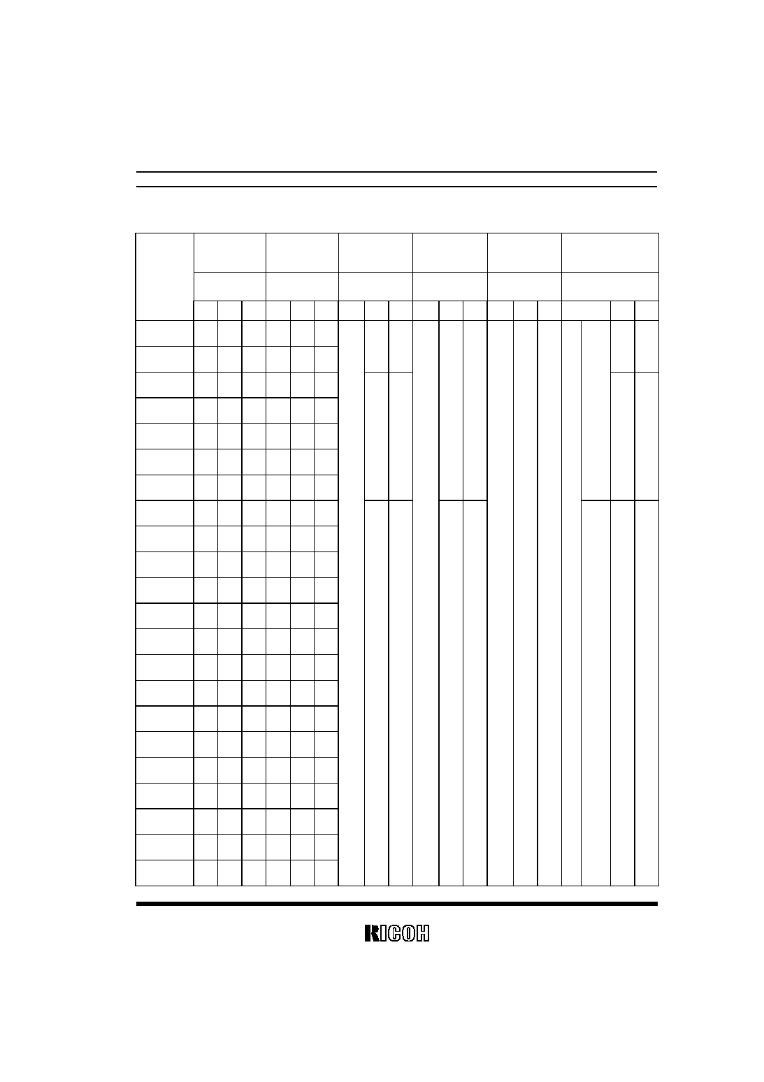
ELECTRICAL CHARACTERISTICS BY DETECTOR THRESHOLD
Detector
Threshold
Hysteresis
Range
Supply Current 1 Supply Current 2 Output Current 1
Output Current 2
Product Code
-V
DET
[V] V
HYS
[V] I
SS
1[µA] I
SS
2[µA] I
OUT
1[mA] I
OUT
2[mA]
Min.
Typ.
Max. Min. Typ. Max.
Condi-
tions Typ. Max.
Condi-
tions Typ. Max.
Condi-
tions Min. Typ. Conditions Min. Typ.
R3112x091A
/C
0.88
2
0.90
0
0.91
8
0.02
7
0.04
5
0.06
3
R3112x101A
/C
0.98
0
1.00
0
1.02
0
0.03
0
0.05
0
0.07
0
0.6
2.0
0.05 0.9
R3112x111A
/C
1.07
8
1.10
0
1.12
2
0.03
3
0.05
5
0.07
7
R3112x121A
/C
1.17
6
1.20
0
1.22
4
0.03
6
0.06
0
0.08
4
R3112x131A
/C
1.27
4
1.30
0
1.32
6
0.03
9
0.06
5
0.09
1
R3112x141A
/C
1.37
2
1.40
0
1.42
8
0.04
2
0.07
0
0.09
8
R3112x151A
/C
1.47
0
1.50
0
1.53
0
0.04
5
0.07
5
0.10
5
0.7
2.5
0.5 2.0
V
DS
=
0.5V
V
DD
=
0.85V
0.2
1.8
R3112x161A
/C
1.56
8
1.60
0
1.63
2
0.04
8
0.08
0
0.11
2
R3112x171A
/C
1.66
6
1.70
0
1.73
4
0.05
1
0.08
5
0.11
9
R3112x181A
/C
1.76
4
1.80
0
1.83
6
0.05
4
0.09
0
0.12
6
R3112x191A
/C
1.86
2
1.90
0
1.93
8
0.05
7
0.09
5
0.13
3
R3112x201A
/C
1.96
0
2.00
0
2.04
0
0.06
0
0.10
0
0.14
0
R3112x211A
/C
2.05
8
2.10
0
2.14
2
0.06
3
0.10
5
0.14
7
R3112x221A
/C
2.15
6
2.20
0
2.24
4
0.06
6
0.11
0
0.15
4
R3112x231A
/C
2.25
4
2.30
0
2.34
6
0.06
9
0.11
5
0.16
1
R3112x241A
/C
2.35
2
2.40
0
2.44
8
0.07
2
0.12
0
0.16
8
R3112x251A
/C
2.45
0
2.50
0
2.55
0
0.07
5
0.12
5
0.17
5
R3112x261A
/C
2.54
8
2.60
0
2.65
2
0.07
8
0.13
0
0.18
2
R3112x271A
/C
2.64
6
2.70
0
2.75
4
0.08
1
0.13
5
0.18
9
R3112x281A
/C
2.74
4
2.80
0
2.85
6
0.08
4
0.14
0
0.19
6
R3112x291A
/C
2.84
2
2.90
0
2.95
8
0.08
7
0.14
5
0.20
3
R3112x301A
/C
2.94
0
3.00
0
3.06
0
0.09
0
0.15
0
0.21
0
V
DD
=
-V
DET
-0.1V
1.0
3.0
V
DD
=
-V
DET
+0.1
V
0.5 2.5
V
DS
=
0.05
V
V
DD
=
0.7V
0.01 0.12 Nch
V
DS
=
0.5V
V
DD
=
1.5V
1.0
3.0
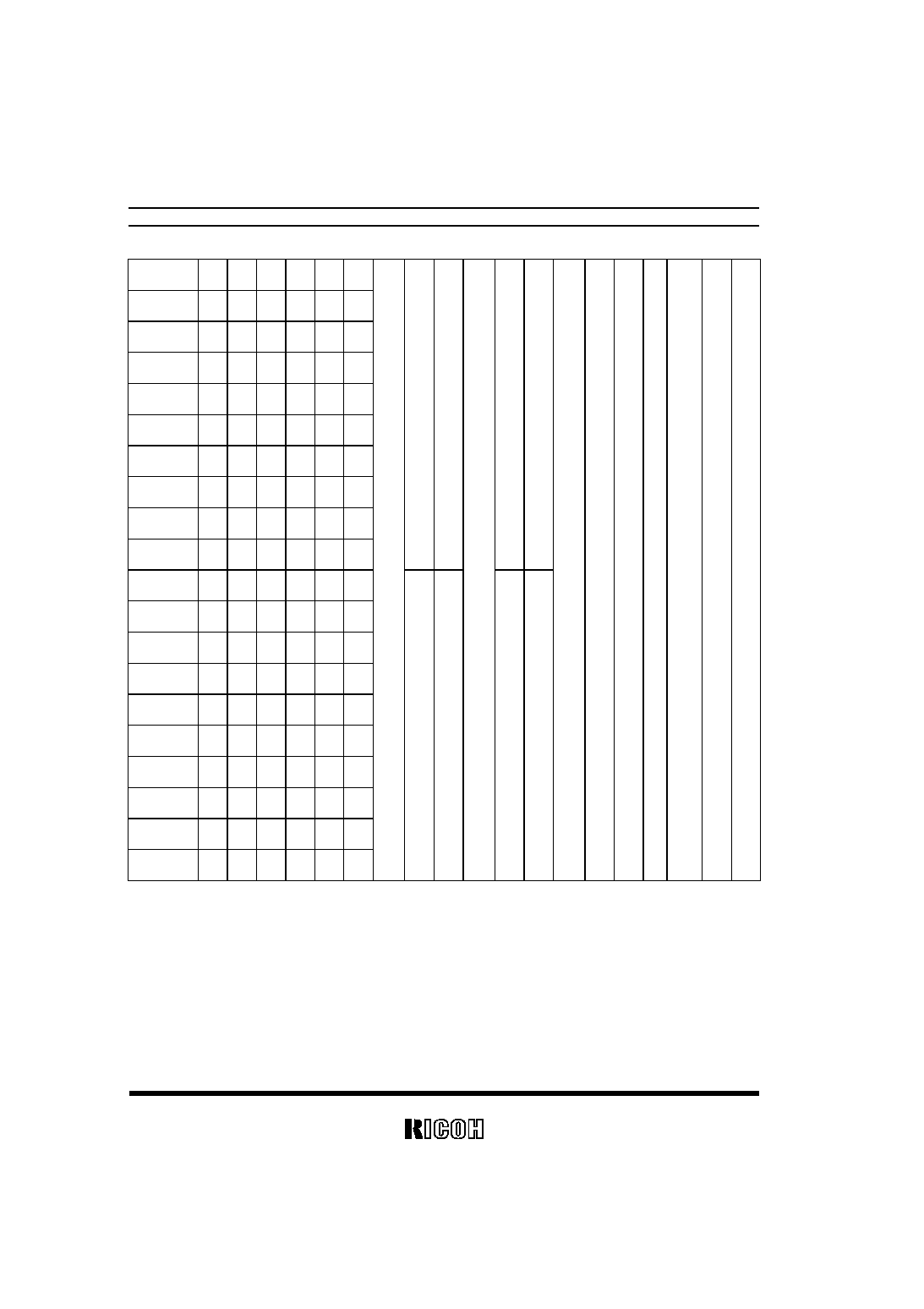
R3112xxx1A/C
12
R3112x311A
/C
3.03
8
3.10
0
3.16
2
0.09
3
0.15
5
0.21
7
R3112x321A
/C
3.13
6
3.20
0
3.26
4
0.09
6
0.16
0
0.22
4
R3112x331A
/C
3.23
4
3.30
0
3.36
6
0.09
9
0.16
5
0.23
1
R3112x341A
/C
3.33
2
3.40
0
3.46
8
0.10
2
0.17
0
0.23
8
R3112x351A
/C
3.43
0
3.50
0
3.57
0
0.10
5
0.17
5
0.24
5
R3112x361A
/C
3.52
8
3.60
0
3.67
2
0.10
8
0.18
0
0.25
2
R3112x371A
/C
3.62
6
3.70
0
3.77
4
0.11
1
0.18
5
0.25
9
R3112x381A
/C
3.72
4
3.80
0
3.87
6
0.11
4
0.19
0
0.26
6
R3112x391A
/C
3.82
2
3.90
0
3.97
8
0.11
7
0.19
5
0.27
3
R3112x401A
/C
3.92
0
4.00
0
4.08
0
0.12
0
0.20
0
0.28
0
1.2
3.0
0.6
2.5
R3112x411A
/C
4.01
8
4.10
0
4.18
2
0.12
3
0.20
5
0.28
7
R3112x421A
/C
4.11
6
4.20
0
4.28
4
0.12
6
0.21
0
0.29
4
R3112x431A
/C
4.21
4
4.30
0
4.38
6
0.12
9
0.21
5
0.30
1
R3112x441A
/C
4.31
2
4.40
0
4.48
8
0.13
2
0.22
0
0.30
8
R3112x451A
/C
4.41
0
4.50
0
4.59
0
0.13
5
0.22
5
0.31
5
R3112x461A
/C
4.50
8
4.60
0
4.69
2
0.13
8
0.23
0
0.32
2
R3112x471A
/C
4.60
6
4.70
0
4.79
4
0.14
1
0.23
5
0.32
9
R3112x481A
/C
4.70
4
4.80
0
4.89
6
0.14
4
0.24
0
0.33
6
R3112x491A
/C
4.80
2
4.90
0
4.99
8
0.14
7
0.24
5
0.34
3
R3112x501A
/C
4.90
0
5.00
0
5.10
0
0.15
0
0.25
0
0.35
0
1.5
3.0
0.6
2.5

R3112xxx1A/C
13
Output Current 3
Minimum Operating
Voltage
CD pin Threshold
Voltage
CD pin Output
Current 1
CD pin Output
Current 2
Resistance for
Output Delay
Detector
Threshold
Tempera-
ture
I
OUT
3[mA] V
DDL
[V] V
TCD
[V] I
CD
1[
µ
µ
µ
µ
A] I
CD
2[
µ
µ
µ
µ
A] R
D
[M
]
-V
DET
/
Topt
[ppm/
∞
∞
∞
∞
C]
Condition Min. Typ. Con-
dition
Max. Con-
dition
Max. Con-
dition
Min. Typ. Max. Con-
dition
Min. Typ. Con-
dition
Min. Typ. Min. Typ. Max. Con-
dition
Typ.
0.29
7
0.49
5
0.69
3
0.33
0
0.55
0
0.77
0
V
DS
=
0.5V
V
DD
=
0.85
V
0.01 400
0.36
3
0.60
5
0.84
7
0.39
6
0.66
0
0.92
4
0.42
9
0.71
5
1.00
1
0.46
2
0.77
0
1.07
8
0.49
5
0.82
5
1.15
5
V
DS
=
0.5V
V
DD
=
0.85
V
0.05 450
0.52
8
0.88
0
1.23
2
0.56
1
0.93
5
1.30
9
0.59
4
0.99
0
1.38
6
0.62
7
1.04
5
1.46
3
0.66
0
1.10
0
1.54
0
0.69
3
1.15
5
1.61
7
0.72
6
1.21
0
1.69
4
0.75
9
1.26
5
1.77
1
0.79
2
1.32
0
1.84
8
0.82
5
1.37
5
1.92
5
0.85
8
1.43
0
2.00
2
0.89
1
1.48
5
2.07
9
0.92
4
1.54
0
2.15
6
0.95
7
1.59
5
2.23
3
Pch
V
DS
=
-21V
V
DD
=
4.5V
1.5 3.5
Topt=
25
∞
C
0.7
-40
∞
C
Topt
85
∞
C
0.8
V
DD
=
(V
DET
)
◊
1.1V
0.99
0
1.65
0
2.31
0
V
DS
=
0.1V
V
DD
=
0.7V
20 70
V
DS
=
0.5V
V
DD
=
1.5V
0.20 500
3.25 6.5 13.0
-40
∞
C
Topt
85
∞
C
±
100
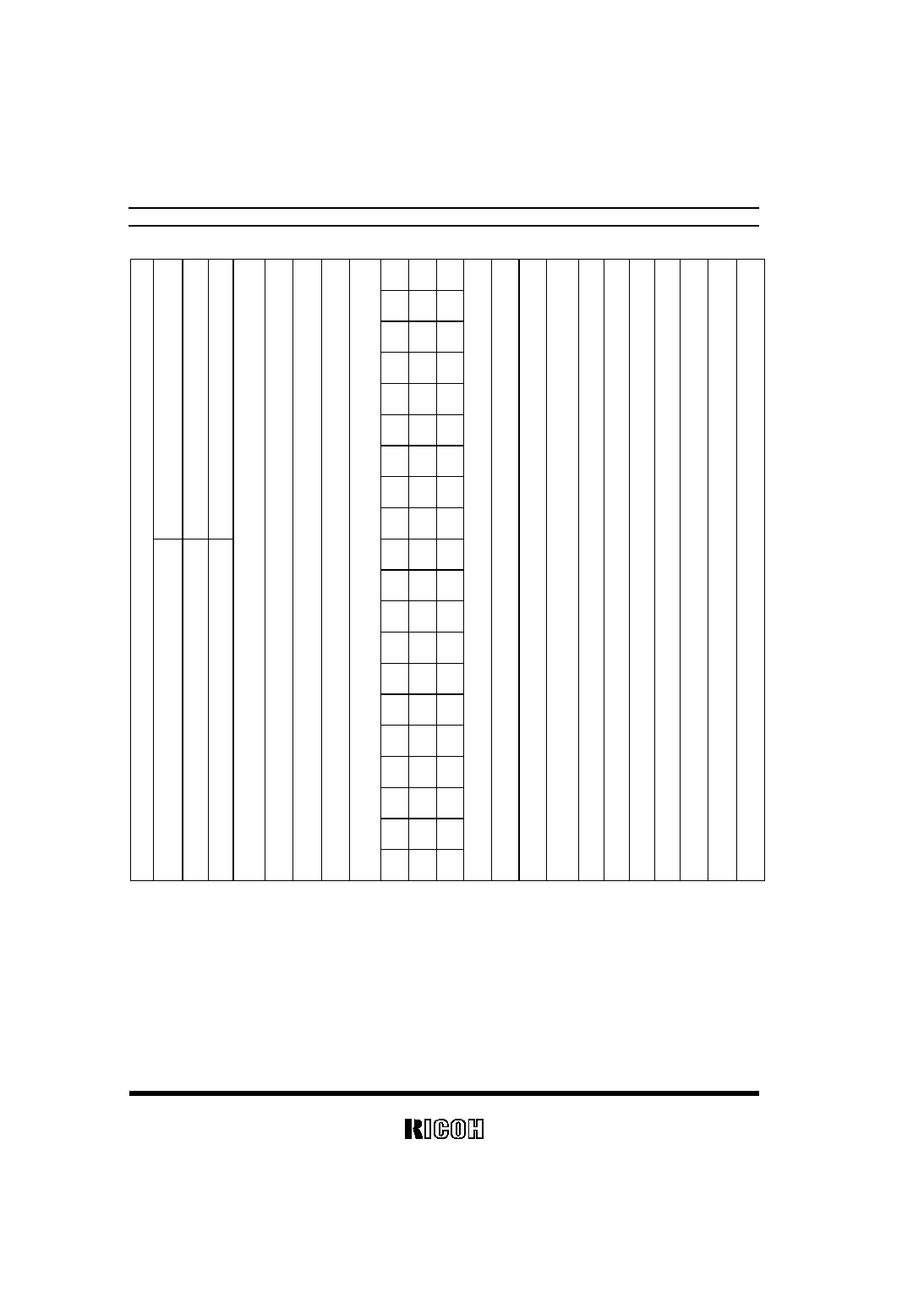
R3112xxx1A/C
14
1.02
3
1.70
5
2.38
7
1.05
6
1.76
0
2.46
4
1.08
9
1.81
5
2.54
1
1.12
2
1.87
0
2.61
8
1.15
5
1.92
5
2.69
5
1.18
8
1.98
0
2.77
2
1.22
1
2.03
5
2.84
9
1.25
4
2.09
0
2.92
6
1.28
7
2.14
5
3.00
3
1.32
0
2.20
0
3.08
0
1.35
3
2.25
5
3.15
7
1.38
6
2.31
0
3.23
4
1.41
9
2.36
5
3.31
1
1.45
2
2.42
0
3.38
8
1.48
5
2.47
5
3.46
5
1.51
8
2.53
0
3.54
2
1.55
1
2.58
5
3.61
9
1.58
4
2.64
0
3.69
6
1.61
7
2.69
5
3.77
3
V
DS
=
-2.1
V
V
DD
=
6.0V
2.0 4.5
1.65
0
2.75
0
3.85
0
R3112xxx1A/C
15
TEST CIRCUITS
*Pull-up circuit is not necessary for CMOS Output type, or R3112xxxxC.
R3112x
V
DD
V
IN
I
SS
GND
R3112x
V
DD
OUT
+5V or V
DD
470k
V
IN
GND
Supply Current Test Circuit
Detector Threshold Test Circuit
V
DD
OUT
V
IN
V
DS
GND
I
OUT
R3112x
V
DD
OUT
V
IN
V
DD
+V
DS
GND
I
OUT
R3112x
Nch Driver Output Current Test Circuit
Pch Driver Output Current Test Circuit
*Apply only to CMOS
V
DD
C
D
OUT
+5V or V
DD
470k
V
IN
GND
V
DS
R3112x
V
DD
C
D
V
IN
GND
V
DS
I
CD
R3112x
CD Pin Threshold Test Circuit
CD Pin Output Current Test Circuit
+V
DET
+2.0 or 0.6V
Input
Voltage
Output Voltage
0.7V
GND
100%
50%
GND
R3112x
V
DD
C
D
O
UT
+5V
470k
V
IN
GND
C
D
Output Delay Time Test Circuit
R3112xxx1A/C
16
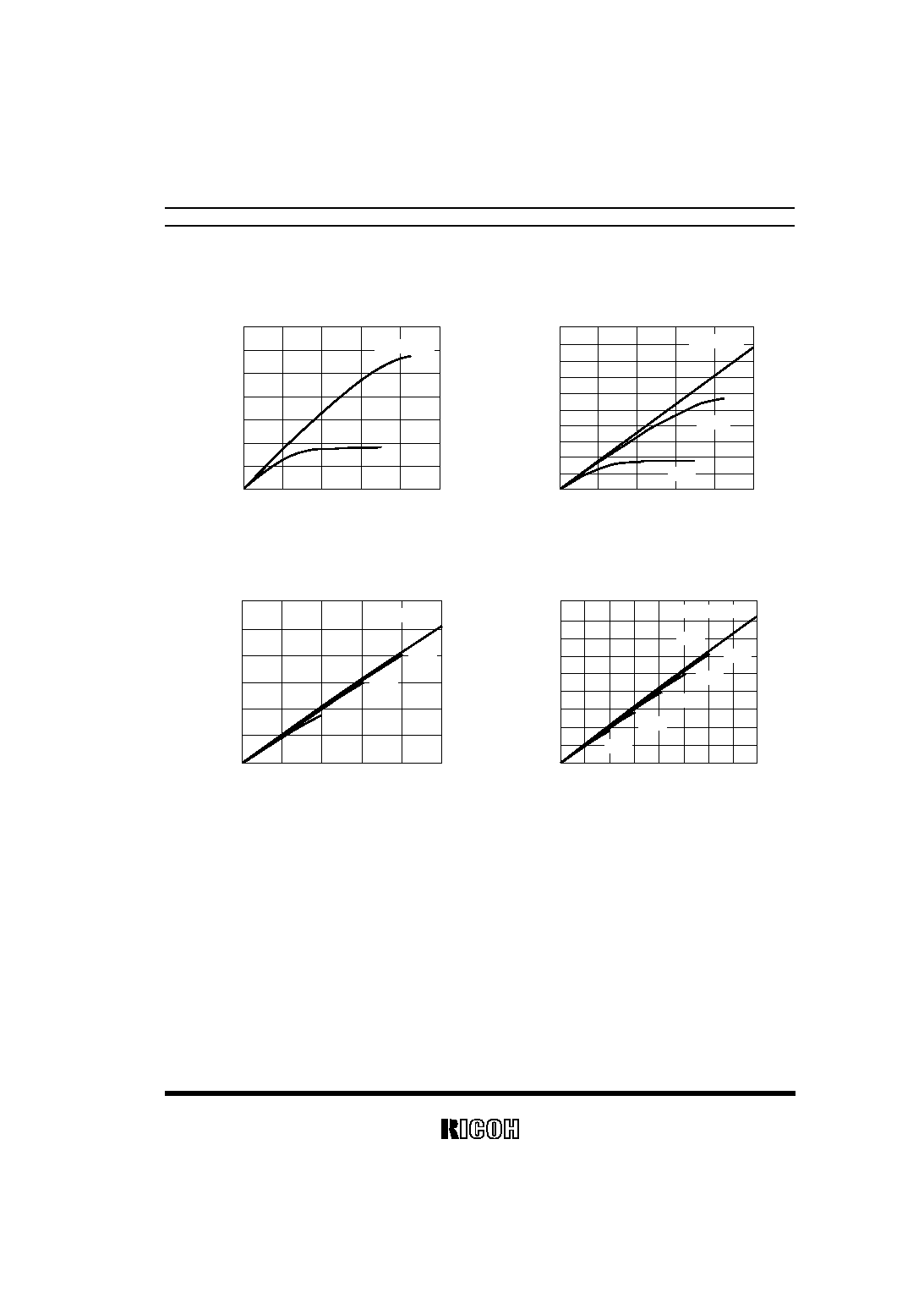
TYPICAL CHARACTERISTICS
1) Supply Current vs. Input Voltage
R3112x091x
R3112x131x
1.5
1.2
0.9
0.6
0.3
0
Input Voltage V
IN
(V)
Supply Current I
ss
(
µ
A)
0
1
2
3
4
5
6
7
Topt=85
∞
C
-40
∞
C
25
∞
C
1.5
1.2
0.9
0.6
0.3
0
Input Voltage V
IN
(V)
Supply Current I
ss
(
µ
A)
0
1
2
3
4
5
6
7
Topt=85
∞
C
-40
∞
C
25
∞
C
R3112x271x
R3112x451x
1.5
1.2
0.9
0.6
0.3
0
Input Voltage V
IN
(V)
Supply Current I
ss
(
µ
A)
0
1
2
3
4
5
6
7
Topt=85
∞
C
-40
∞
C
25
∞
C
2.0
1.6
1.2
0.8
0.4
0
Input Voltage V
IN
(V)
Supply Current I
ss
(
µ
A)
0
1
2
3
4
5
6
7
Topt=85
∞
C
-40
∞
C
25
∞
C
2) Detector Threshold vs. Temperature
R3112x091x
R3112x131x
R3112xxx1A/C
17
0.98
0.88
0.86
Temperature Topt(
∞
C)
Detector Threshold/Released Voltage
V
DET
(V)
-50
-25
75
100
0
25
50
0.90
0.92
0.94
0.96
+V
DET
-V
DET
1.42
1.28
1.26
Temperature Topt(
∞
C)
Detector Threshold/Released Voltage
V
DET
(V)
-50
-25
75
100
0
25
50
1.30
1.32
1.34
1.36
1.38
1.40
+V
DET
-V
DET

R3112xxx1A/C
18
R3112x271x
R3112x451x
2.90
2.65
2.60
Temperature Topt(
∞
C)
Detector Threshold/Released Voltage
V
DET
(V)
-50
-25
75
100
0
25
50
2.70
2.75
2.80
2.85
+V
DET
-V
DET
4.75
4.40
4.35
Temperature Topt(
∞
C)
Detector Threshold/Released Voltage
V
DET
(V)
-50
-25
75
100
0
25
50
4.45
4.50
4.55
4.60
4.65
4.70
+V
DET
-V
DET
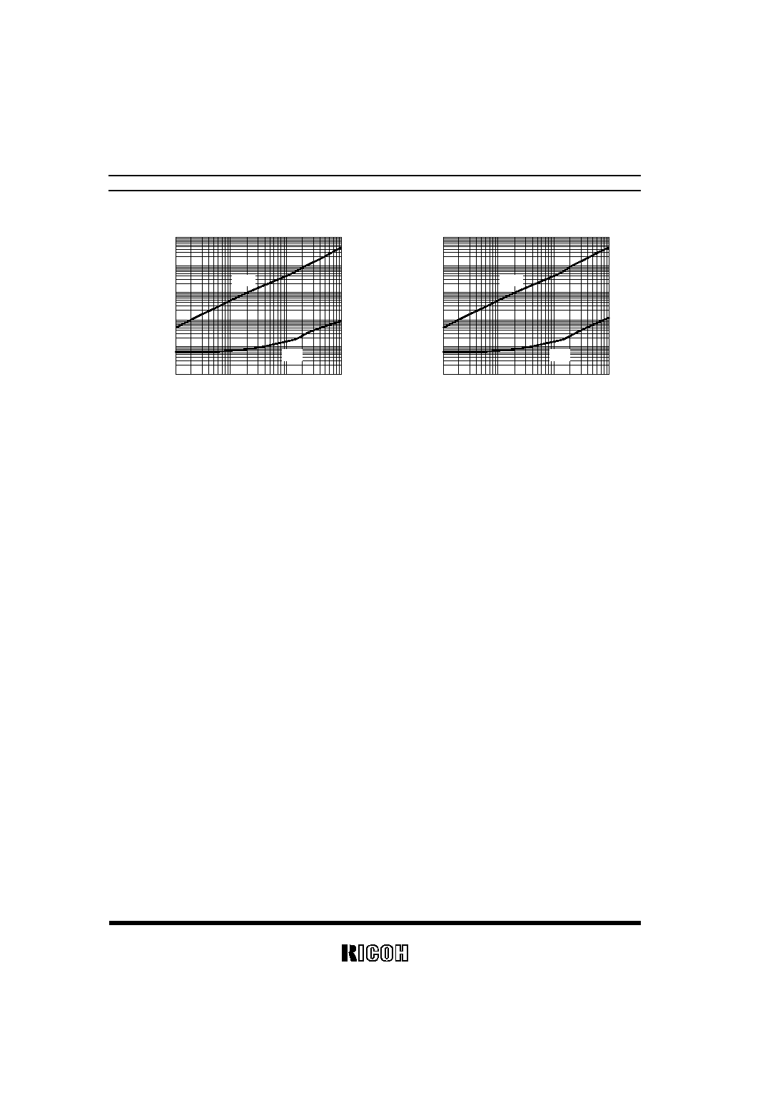
3) Output Voltage vs. Input Voltage
R3112x091x
R3112x091A
1.0
0.8
0.6
0.4
0.2
0.0
Input Voltage V
IN
(V)
Output Voltage V
OUT
(V)
0
0.2
0.8
1
0.4
0.6
Nch Output Type: V
DD
pull up
Topt=-40
∞
C
25
∞
C
85
∞
C
6.0
5.0
4.0
3.0
2.0
0.0
Input Voltage V
IN
(V)
Output Voltage V
OUT
(V)
0
0.2
0.8
1
0.4
0.6
1.0
5V pull up via 470k
Topt=-40
∞
C
25
∞
C
85
∞
C
R3112x131x
R3112x131A
1.5
1.2
0.9
0.6
0.3
0
Input Voltage V
IN
(V)
Output Voltage V
OUT
(V)
0
0.3
1.2
1.5
0.6
0.9
Nch Output Type: V
DD
pull up
Topt=-40
∞
C
25
∞
C
85
∞
C
6.0
5.0
4.0
3.0
2.0
0.0
Input Voltage V
IN
(V)
Output Voltage V
OUT
(V)
0
0.3
1.2
1.5
0.6
0.9
1.0
5V pull up via 470k
Topt=-40
∞
C
25
∞
C
85
∞
C
R3112xxx1A/C
19
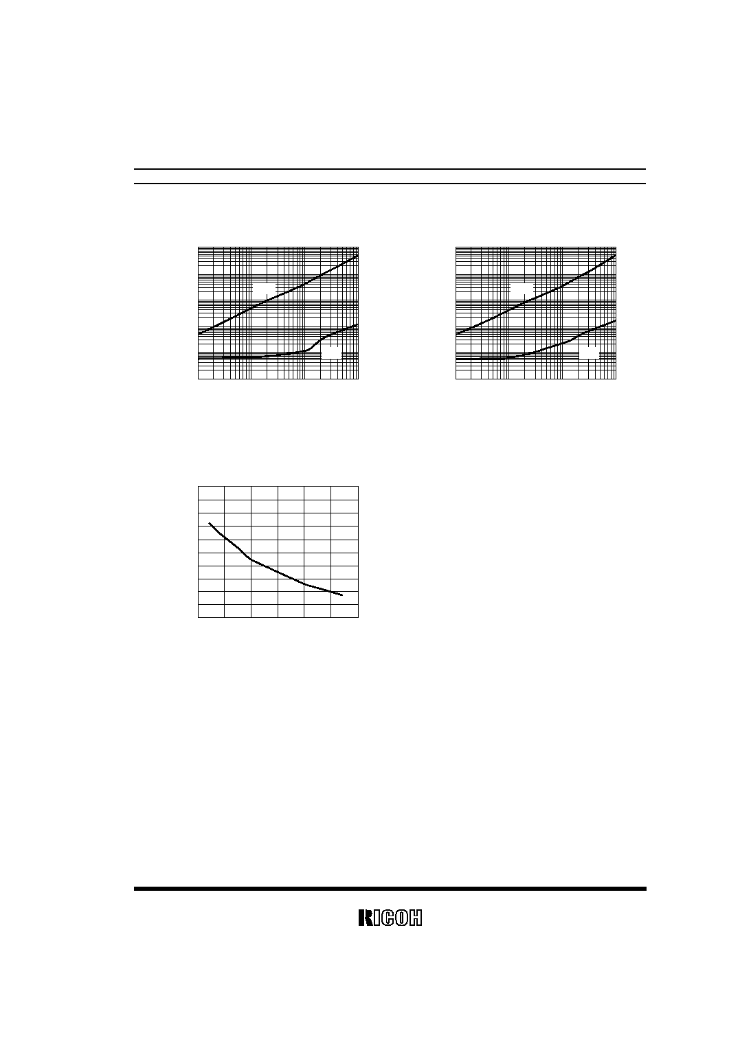
R3112x271x
R3112x271A
3.0
2.5
2.0
1.5
1.0
0.5
0.0
Input Voltage V
IN
(V)
Output Voltage V
OUT
(V)
0.0
0.5
1.0
1.5
2.0
2.5
3.0
Nch Output Type: V
DD
pull up
Topt=-40
∞
C
25
∞
C
85
∞
C
6.0
5.0
4.0
3.0
2.0
1.0
0.0
Input Voltage V
IN
(V)
Output Voltage V
OUT
(V)
0.0
0.5
1.0
1.5
2.0
2.5
3.0
5V pull up via 470k
Topt=-40
∞
C
25
∞
C
85
∞
C
R3112x451x
R3112x451A
5.0
4.5
0.5
1.0
1.5
2.0
2.5
3.0
3.5
4.0
0.0
Input Voltage V
IN
(V)
Output Voltage V
OUT
(V)
0.0 0.5 1.0 1.5 2.0 2.5 3.0 3.5 4.0 4.5 5.0
Nch Output Type: V
DD
pull up
Topt=-40
∞
C
25
∞
C
85
∞
C
6.0
5.0
4.0
3.0
2.0
1.0
0.0
Input Voltage V
IN
(V)
Output Voltage V
OUT
(V)
0.0 0.5 1.0
2.0
3.5 4.0
5.0
2.5 3.0
1.5
4.5
5V pull up via 470k
Topt=-40
∞
C
25
∞
C
85
∞
C
4) Nch Driver Output Current vs. V
DS
R3112x091x
R3112x131x
1.2
1.0
0.6
0.4
0.2
0
V
DS
(V)
Output Current I
OUT
(mA)
0
0.2
0.4
0.6
0.8
1
0.8
Topt=25
∞
C
V
DD
=0.85V
0.7V
2.5
2.0
1.5
1.0
0.5
0
V
DS
(V)
Output Current I
OUT
(mA)
0
0.2
0.4
0.6
0.8
1
Topt=25
∞
C
V
DD
=1.0V
0.85V
0.7V

R3112xxx1A/C
20
R3112x271x
R3112x451x
20
16
12
8
4
0
V
DS
(V)
Output Current I
OUT
(mA)
0
0.5
1
1.5
2
2.5
Topt=25
∞
C
V
DD
=2.5V
1.0V
1.5V
2.0V
20
16
12
8
4
0
V
DS
(V)
Output Current I
OUT
(mA)
0
0.5
1.5
3
3.5
4
2
1
2.5
Topt=25
∞
C
V
DD
=2.5V
V
DD
=3.0V
V
DD
=4.0V
V
DD
=3.5V
1.0V
1.5V
2.0V
5) Nch Driver Output Current vs. Input Voltage
R3112x091x
R3112x131x
2.0
1.5
1.0
0.5
0.0
Input Voltage V
IN
(V)
Output Current I
OUT
(mA)
0
0.2
0.4
0.6
0.8
1
Topt=25
∞
C
-40
∞
C
85
∞
C
5
4
2
1
0
Input Voltage V
IN
(V)
Output Current I
OUT
(mA)
0
0.3
0.6
0.9
1.2
1.5
3
Topt=-40
∞
C
85
∞
C
25
∞
C
R3112x271x
R3112x451x
5
4
0
Input Voltage V
IN
(V)
Output Current I
OUT
(mA)
0
0.5
3
1
1.5
2
2.5
3
2
1
Topt=-40
∞
C
85
∞
C
25
∞
C
5
4
0
Input Voltage V
IN
(V)
Output Current I
OUT
(mA)
0
1
2
3
4
5
3
2
1
Topt=-40
∞
C
85
∞
C
25
∞
C

R3112xxx1A/C
21
6) Pch Driver Output Current vs. Input Voltage
R3112x091C
R3112x131C
6
1
0
Input Voltage V
IN
(V)
Output Current I
OUT
(mA)
0
1
4
6
7
5
3
2
2
3
4
5
Topt=25
∞
C
V
DS
=-2.1V
-0.5V
-1.0V
-1.5V
6
1
0
Input Voltage V
IN
(V)
Output Current I
OUT
(mA)
0
1
4
6
7
5
3
2
2
3
4
5
Topt=25
∞
C
V
DS
=-2.1V
-0.5V
-1.0V
-1.5V
R3112x271C
R3112x451C
6
1
0
Input Voltage V
IN
(V)
Output Current I
OUT
(mA)
0
1
4
6
7
5
3
2
2
3
4
5
Topt=25
∞
C
V
DS
=-2.1V
-0.5V
-1.0V
-1.5V
6
1
0
Input Voltage V
IN
(V)
Output Current I
OUT
(mA)
0
1
4
6
7
5
3
2
2
3
4
5
Topt=25
∞
C
V
DS
=-2.1V
-0.5V
-1.0V
-1.5V
7) C
D
Pin Threshold Voltage vs. Temperature
R3112x091x
R3112x131x
R3112xxx1A/C
22
0.8
0.3
0.2
Temperature Topt(
∞
C)
C
D
Pin Threshold Voltage V
TCD
(V)
-50
-25
75
100
0
25
50
0.4
0.5
0.6
0.7
V
DD
=0.99V
1.0
0.5
0.4
Temperature Topt(
∞
C)
C
D
Pin Threshold Voltage V
TCD
(V)
-50
-25
75
100
0
25
50
0.6
0.7
0.8
0.9
V
DD
=1.43V

R3112xxx1A/C
23
R3112x271x
R3112x451x
1.9
1.4
1.3
Temperature Topt(
∞
C)
C
D
Pin Threshold Voltage V
TCD
(V)
-50
-25
75
100
0
25
50
1.5
1.6
1.7
1.8
V
DD
=2.97V
2.9
2.4
2.3
Temperature Topt(
∞
C)
C
D
Pin Threshold Voltage V
TCD
(V)
-50
-25
75
100
0
25
50
2.5
2.6
2.7
2.8
V
DD
=4.95V
8) C
D
Pin Output Current vs. Input Voltage
R3112x091x
R3112x131x
1.0
0.8
0.4
0.2
0
Input Voltage V
IN
(V)
C
D
Pin Output Current I
CD
(mA)
0
0.2
0.4
0.6
0.8
1
0.6
V
DS
=0.5V
Topt=-40
∞
C
85
∞
C
25
∞
C
1.0
0.8
0.4
0.2
0
Input Voltage V
IN
(V)
C
D
Pin Output Current I
CD
(mA)
0
0.3
0.6
0.9
1.2
1.5
0.6
V
DS
=0.5V
Topt=-40
∞
C
85
∞
C
25
∞
C
R3112x271x
R3112x451x
1.0
0.8
0.4
0.2
0
Input Voltage V
IN
(V)
C
D
Pin Output Current I
CD
(mA)
0
0.5
1
2.5
2
3
1.5
0.6
V
DS
=0.5V
Topt=-40
∞
C
85
∞
C
25
∞
C
1.0
0.8
0.4
0.2
0
Input Voltage V
IN
(V)
C
D
Pin Output Current I
CD
(mA)
0
1
2
4
3
5
0.6
V
DS
=0.5V
Topt=-40
∞
C
85
∞
C
25
∞
C

R3112xxx1A/C
24
R3112xxx1A/C
25
9) C
D
Pin Output Current vs. V
DS (Topt=25∞C)
R3112x091x
R3112x131x
0.7
0.6
0.3
0.2
0.1
0
V
DS
(V)
C
D
Pin Output Current I
CD
(mA)
0
0.2
0.4
0.6
0.8
1
0.4
0.5
Topt=25
∞
C
V
DD
=0.85V
0.7V
1.0
0.7
0.3
0.2
0.1
0
V
DS
(V)
C
D
Pin Output Current I
CD
(mA)
0
0.2
0.4
0.6
0.8
1
0.6
0.8
0.9
0.4
0.5
Topt=25
∞
C
V
DD
=1.0V
0.85V
0.7V
R3112x271x
R3112x451x
3.0
2.0
1.0
0.5
0
V
DS
(V)
C
D
Pin Output Current I
CD
(mA)
0
0.5
1
1.5
2
2.5
2.5
1.5
Topt=25
∞
C
V
DD
=2.5V
1.0V
1.5V
2.0V
4.5
2.0
1.0
0.5
0
V
DS
(V)
C
D
Pin Output Current I
CD
(mA)
0
0.5
1.5
2.5
3.5
4
1
2
3
2.5
3.0
3.5
4.0
1.5
Topt=25
∞
C
V
DD
=4.0V
1.0V
2.0V
1.5V
2.5V
3.5V
3.0V
10) Output Delay Time vs. External Capacitance (Topt=25∞C)
R3112x091x
R3112x131x
R3112xxx1A/C
26
1000
0.01
External Capacitance C
D
(
µ
F)
Output Deley Time tx(ms)
0.0001
0.001
0.01
0.1
0.1
1
10
100
Topt=25
∞
C
t
PHL
t
D
1000
0.01
External Capacitance C
D
(
µ
F)
Output Delay tx(ms)
0.0001
0.001
0.01
0.1
0.1
1
10
100
Topt=25
∞
C
t
PHL
t
D
R3112xxx1A/C
27
R3112x271x
R3112x451x
1000
0.01
External Capacitance C
D
(
µ
F)
Output Delay Time tx(ms)
0.0001
0.001
0.01
0.1
0.1
1
10
100
Topt=25
∞
C
t
PHL
t
D
1000
0.01
External Capacitance C
D
(
µ
F)
Output Delay Time tx(ms)
0.0001
0.001
0.01
0.1
0.1
1
10
100
Topt=25
∞
C
t
PHL
t
D
11) Delay Circuit Resistance vs. Temperature
R3112xxx1x
13
4
3
Temperature Topt(
∞
C)
Delay Circuit Resistance R
D
(M
)
-50
-25
75
100
0
25
50
7
6
5
8
9
12
11
10
R3112xxx1A/C
28
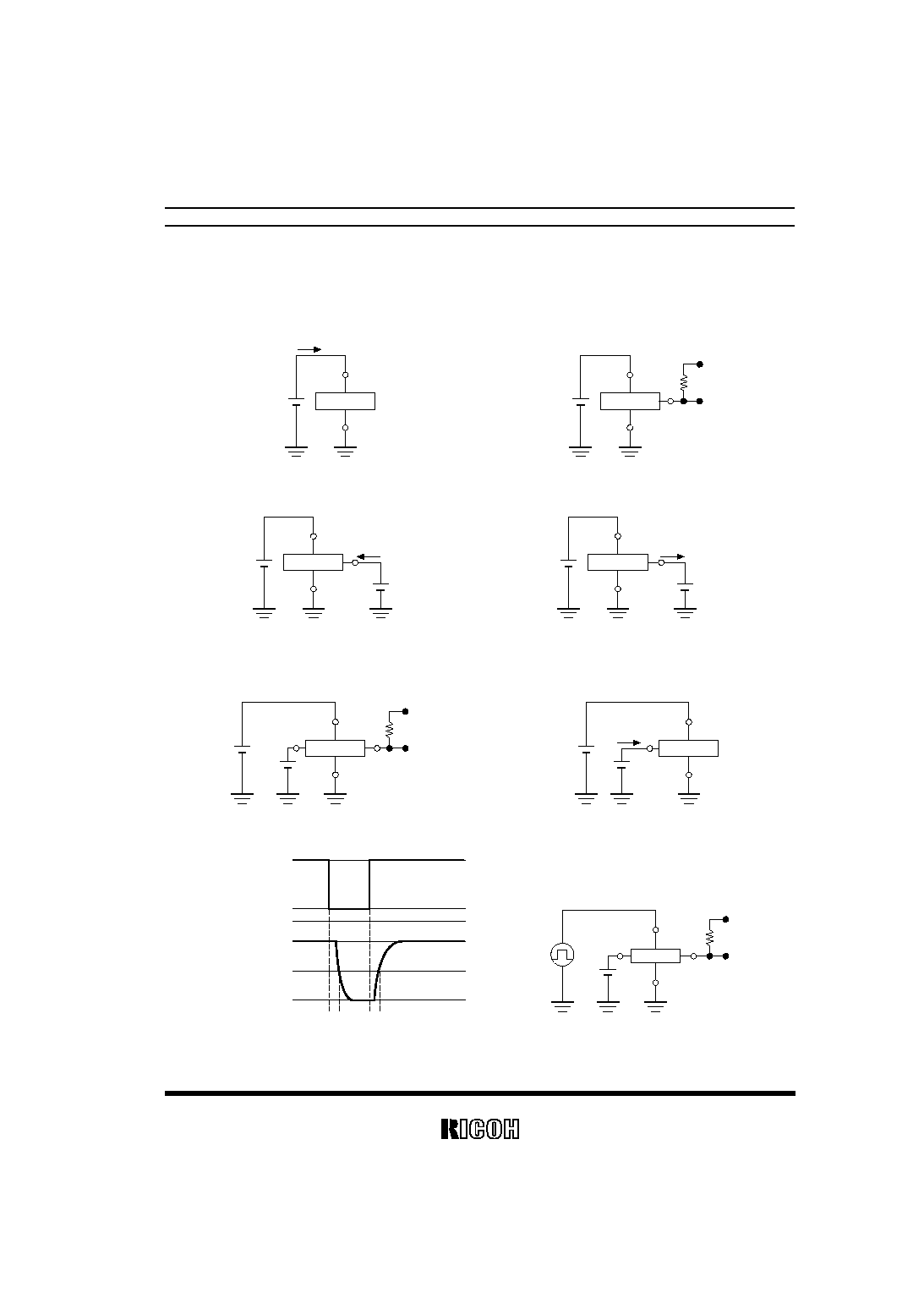
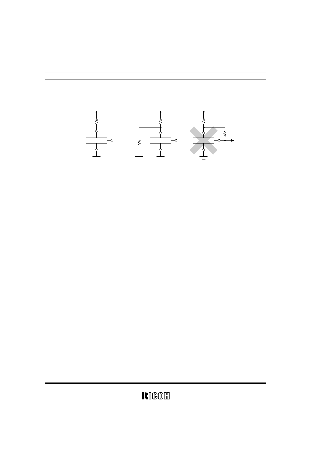
TECHNICAL NOTES
V
DD
R
V
DD
GND
OUT
R3112x
V
DD
R1
R2
V
DD
GND
OUT
R3112x
V
DD
R1
R2
V
DD
GND
OUT
R3112x
Figure A
Figure B
Figure C
When R3112xxx1A (Nch open drain output type) is used in Figure A or Figure B, if impedance of
voltage supply pIn, V
DD
and V
DD
of this IC is large, detector threshold level would shift by voltage
dropdown caused by the consumption current of the IC itself. Released voltage may also shift and delay
time for start-up might be generated by this usage.
When R3112xxx1C (CMOS output type) is used in Figure A or Figure B, Output level could be un-
stable by cross conduction current which is generated at detector threshold level or at released voltage
level, therefore, do not use R3112xxx1C with the connection in Figure A or Figure B.
The connection in Figure C may cause the oscillation in both R3112xxx1C (CMOS Output) and
R3112xxx1A (Nch Open Drain Output), therefore do not use R3112xxx1x Series with the connection in
Figure C.