
LOW VOLTAGE DETECTOR WITH
OUTPUT DELAY
R3115Z SERIES
1
R3115Z_E.doc/2003/05/06
NO. EA-098-0301
OUTLINE
The R3115Z Series are CMOS-based voltage detector ICs with high detector threshold accuracy and ultra-low sup-
ply current, which can be operated at an extremely low voltage and is used for system reset as an example.
Each of these ICs consists of a voltage reference unit, a comparator, resistor net for detector threshold setting, an
output driver, a hysteresis circuit, and an output delay circuit. The detector threshold is fixed with high accuracy inter-
nally and does not require any adjustment. Two output types, Nch open drain type and CMOS type are available.
Since the package is WL-CSP, high density mounting on boards is possible.
FEATURES
∑ Built-in Output Delay Circuit ..................................................... Typ. 100ms with an external capacitor: 0.022µF
∑ Ultra-low Supply Current
..........................................................................
Typ. 0.8µA (V
DD
=3.5V)
∑ Wide Range of Operating Voltage
...........................................................
0.76.0V (Topt=25∞C)
∑ Detector Threshold..................................................................... Stepwise setting with a step of 0.1V in the range of
0.9V to 5.0V is possible.
∑ High Accuracy Detector Threshold
.......................................................
±2.0%
∑ Low Temperature-Drift Coefficient of Detector Threshold
........
Typ. ±100ppm/∞C
∑ Two Output Types
.........................................................................................
Nch Open Drain and CMOS
∑ Two Types of Packages................................................................ WL-CSP
APPLICATIONS
∑ Micro controller and Logic Circuit Reset
∑ Battery Checker
∑ Window Comparator
∑ Wave Shaping Circuit
∑ Battery Back-up Circuit
∑ Power Failure Detector
R3115Z
2
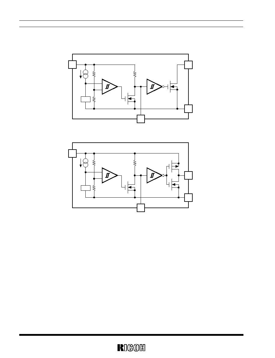
BLOCK DIAGRAMS
∑ Nch Open Drain Output (R3115Zxx1A)
V
DD
OUT
GND
C
D
R
D
-
+
Vref
∑ CMOS Output (R3115Zxx1C)
V
DD
OUT
GND
C
D
R
D
-
+
Vref
R3115Z
3
SELECTION GUIDE
The detector threshold, the output type, and the taping type of R3115Z Series can be designated at the users' re-
quest by specifying the part number as follows;
R3115Z
xx
1
x
-
xx
Part Number
a b c
Code
Contents
a
Setting Detector Threshold (-V
DET
);
Stepwise setting with a step of 0.1V in the range of 0.9V to 5.0V is possible.
b
Designation of Output Type;
A: Nch Open Drain
C: CMOS
c
Designation of Taping Type;
TR is prescribed as standard directions. (Refer to Taping Specifications)
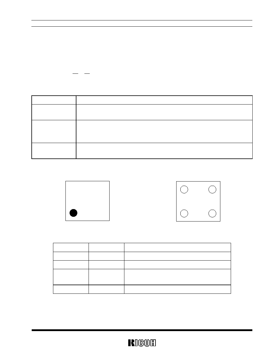
PIN CONFIGURATIONS
V
DD
4
GND 1
3 OUT
Mark Side
2 C
D
OUT
C
D
V
DD
Bump Side
GND
PIN DESCRIPTIONS
Pin No.
Symbol
Description
1
GND
Ground Pin
2
C
D
Pin for External Capacitor (for setting output delay)
3
OUT
Output Pin (Output "L" at detector threshold, Out-
put "H" at released voltage)
4
V
DD
Voltage Supply Pin

R3115Z
4
ABSOLUTE MAXIMUM RATINGS
Symbol
Item
Rating
Unit
V
DD
Supply Voltage
6.5
V
V
OUT1
Output Voltage (CMOS)
V
SS
-0.3V
DD
+0.3
V
V
OUT2
Output Voltage (Nch)
V
SS
-0.36.5
V
I
OUT
Output Current
20
mA
Topt
Operating Temperature Range
-4085
∞C
Tstg
Storage Temperature Range
-55125
∞C
ABSOLUTE MAXIMUM RATINGS
Absolute Maximum ratings are threshold limit values that must not be exceeded ever for an instant under any condi-
tions. Moreover, such values for any two items must not be reached simultaneously. Operation above these absolute
maximum ratings may cause degradation or permanent damage to the device. These are stress ratings only and do
not necessarily imply functional operation below these limits.
Power Dissipation
Power dissipation depends on the condition of the mounting on board, the experiment result below is just an example.
WL-CSP-4 Power Dissipation Example
Conditions: Mounted on board (Wind velocity: 0m/s)
Board: FR-4 (double-layer)
Board Size: 40mm◊40mm◊t1.6mm
Wire rate: 50%
Result: 530mW
Thermal Resistance: 186∞C/W
Temperature Topt(
∞C)
P
D
(mW)
0
0
100
200
300
400
500
600
700
25
50
75
100
125
R3115Z
5
ELECTRICAL CHARACTERISTICS
∑ R3115Z091A/C
Topt=25∞C
Symbol
Item
Conditions
Min.
Typ.
Max.
Unit
-V
DET
Detector Threshold
0.882
0.900
0.918
V
V
HYS
Detector Threshold Hysteresis
0.027
0.045
0.063
V
V
DD
=0.8V
0.6
2.0
I
SS
Supply Current
V
DD
=1.9V
0.5
2.0
µ
A
V
DDH
Maximum Operating Voltage
6.0
V
Topt=25∞C
0.7
V
DDL
Minimum Operating
Voltage*
Note1
-40∞C Topt 85∞C
0.8
V
V
DS
=0.05V, V
DD
=0.70V
10
120
µA
Nch
V
DS
=0.50V, V
DD
=0.85V
0.05
0.90
mA
I
OUT
Output Current
(Driver Output Pin)
Pch
V
DS
=-2.1V, V
DD
=4.5V
1.0
3.5
mA
V
TCD
CD pin Threshold Voltage
V
DD
=0.99V
0.396
0.495
0.594
V
V
DS
=0.10V, V
DD
=0.70V
2
70
I
CD
CD pin Output Current
V
DS
=0.50V, V
DD
=0.85V
10
400
µA
R
D
Output Delay Resistance
3.25
6.50
13.00
M
-V
DET
/
Topt
Detector Threshold
Temperature Coefficient
-40∞C Topt 85∞C
±100
ppm/
∞C

R3115Z
6
∑ R3115Z271A/C
Topt=25∞C
Symbol
Item
Conditions
Min.
Typ.
Max.
Unit
-V
DET
Detector Threshold
2.646
2.700
2.754
V
V
HYS
Detector Threshold Hysteresis
0.081
0.135
0.189
V
V
DD
=2.6V
1.0
3.0
I
SS
Supply Current
V
DD
=3.7V
0.5
2.5
µ
A
V
DDH
Maximum Operating Voltage
6.0
V
Topt=25∞C
0.7
V
DDL
Minimum Operating
Voltage*
Note1
-40∞C Topt85∞C
0.8
V
V
DS
=0.05V, V
DD
=0.70V
10
120
µ
A
Nch
V
DS
=0.50V, V
DD
=1.50V
1.0
3.0
mA
I
OUT
Output Current
(Driver Output Pin)
Pch
V
DS
=-2.1V, V
DD
=4.5V
1.0
3.5
mA
V
TCD
CD pin Threshold Voltage
V
DD
=2.97V
1.188
1.485
1.782
V
V
DS
=0.1V, V
DD
=0.7V
2.0
70.0
I
CD
CD pin Output Current
V
DS
=0.5V, V
DD
=1.5V
200
500
µA
R
D
Output Delay Resistance
3.25
6.50
13.00
M
-V
DET
/
Topt
Detector Threshold
Temperature Coefficient
-40∞C Topt85∞C
±100
ppm/
∞C
R3115Z
7
∑ R3115Z501A/C
Topt=25∞C
Symbol
Item
Conditions
Min.
Typ.
Max.
Unit
-V
DET
Detector Threshold
4.900
5.000
5.100
V
V
HYS
Detector Threshold Hysteresis
0.150
0.250
0.350
V
V
DD
=4.9V
1.5
3.0
I
SS
Supply Current
V
DD
=6.0V
0.6
2.5
µ
A
V
DDH
Maximum Operating Voltage
6.0
V
Topt=25∞C
0.7
V
DDL
Minimum Operating
Voltage*
Note1
-40∞C Topt85∞C
0.8
V
V
DS
=0.05V, V
DD
=0.70V
10
120
µ
A
Nch
V
DS
=0.50V, V
DD
=1.50V
1.0
3.0
mA
I
OUT
Output Current
(Driver Output Pin)
Pch V
DS
=-2.1V, V
DD
=6.0V
1.5
4.5
mA
V
TCD
CD pin Threshold Voltage
V
DD
=5.50V
2.200
2.750
3.300
V
V
DS
=0.1V, V
DD
=0.7V
2.0
70.0
I
CD
CD pin Output Current
V
DS
=0.5V, V
DD
=1.5V
200
500
µA
R
D
Output Delay Resistance
3.25
6.50
13.00
M
-V
DET
/
Topt
Detector Threshold
Temperature Coefficient
-40∞CTopt85∞C
±100
ppm/
∞C
*Note 1: Minimum Operating Voltage means the value of input voltage when output voltage maintains 0.1V or
less.
(In the case of Nch Open Drain Type, Output pin is pulled up with a resistance of 470k
to 5.0V.)
R3115Z
8
ELECTRICAL CHARACTERISTICS BY DETECTOR THRESHOLD
Detector
Threshold
Hysteresis
Range
Supply Current 1 Supply Current 2 Output Current 1
Output Current 2
Product Code
-V
DET
[V]
V
HYS
[V]
I
SS1
[µA]
I
SS2
[µA]
I
OUT1
[mA]
I
OUT2
[mA]
Min. Typ. Max. Min. Typ. Max.
Condi-
tion
Typ. Max.
Condi-
tion
Typ. Max.
Condi-
tion
Min. Typ. Conditions Min. Typ.
R3115Z091A/C 0.882 0.900 0.918 0.027 0.045 0.063
R3115Z101A/C 0.980 1.000 1.020 0.030 0.050 0.070
0.6
2.0
0.05
0.9
R3115Z111A/C 1.078 1.100 1.122 0.033 0.055 0.077
R3115Z121A/C 1.176 1.200 1.224 0.036 0.060 0.084
R3115Z131A/C 1.274 1.300 1.326 0.039 0.065 0.091
R3115Z141A/C 1.372 1.400 1.428 0.042 0.070 0.098
R3115Z151A/C 1.470 1.500 1.530 0.045 0.075 0.105
0.7
2.5
0.5
2.0
V
DS
=
0.5V
V
DD
=
0.85V
0.2
1.8
R3115Z161A/C 1.568 1.600 1.632 0.048 0.080 0.112
R3115Z171A/C 1.666 1.700 1.734 0.051 0.085 0.119
R3115Z181A/C 1.764 1.800 1.836 0.054 0.090 0.126
R3115Z191A/C 1.862 1.900 1.938 0.057 0.095 0.133
R3115Z201A/C 1.960 2.000 2.040 0.060 0.100 0.140
R3115Z211A/C 2.058 2.100 2.142 0.063 0.105 0.147
R3115Z221A/C 2.156 2.200 2.244 0.066 0.110 0.154
R3115Z231A/C 2.254 2.300 2.346 0.069 0.115 0.161
R3115Z241A/C 2.352 2.400 2.448 0.072 0.120 0.168
R3115Z251A/C 2.450 2.500 2.550 0.075 0.125 0.175
R3115Z261A/C 2.548 2.600 2.652 0.078 0.130 0.182
R3115Z271A/C 2.646 2.700 2.754 0.081 0.135 0.189
R3115Z281A/C 2.744 2.800 2.856 0.084 0.140 0.196
R3115Z291A/C 2.842 2.900 2.958 0.087 0.145 0.203
R3115Z301A/C 2.940 3.000 3.060 0.090 0.150 0.210
1.0
3.0
0.5
2.5
R3115Z311A/C 3.038 3.100 3.162 0.093 0.155 0.217
R3115Z321A/C 3.136 3.200 3.264 0.096 0.160 0.224
R3115Z331A/C 3.234 3.300 3.366 0.099 0.165 0.231
R3115Z341A/C 3.332 3.400 3.468 0.102 0.170 0.238
R3115Z351A/C 3.430 3.500 3.570 0.105 0.175 0.245
R3115Z361A/C 3.528 3.600 3.672 0.108 0.180 0.252
R3115Z371A/C 3.626 3.700 3.774 0.111 0.185 0.259
R3115Z381A/C 3.724 3.800 3.876 0.114 0.190 0.266
R3115Z391A/C 3.822 3.900 3.978 0.117 0.195 0.273
R3115Z401A/C 3.920 4.000 4.080 0.120 0.200 0.280
1.2
3.0
0.6
2.5
R3115Z411A/C 4.018 4.100 4.182 0.123 0.205 0.287
R3115Z421A/C 4.116 4.200 4.284 0.126 0.210 0.294
R3115Z431A/C 4.214 4.300 4.386 0.129 0.215 0.301
R3115Z441A/C 4.312 4.400 4.488 0.132 0.220 0.308
R3115Z451A/C 4.410 4.500 4.590 0.135 0.225 0.315
R3115Z461A/C 4.508 4.600 4.692 0.138 0.230 0.322
R3115Z471A/C 4.606 4.700 4.794 0.141 0.235 0.329
R3115Z481A/C 4.704 4.800 4.896 0.144 0.240 0.336
R3115Z491A/C 4.802 4.900 4.998 0.147 0.245 0.343
R3115Z501A/C 4.900 5.000 5.100 0.150 0.250 0.350
V
DD
=
-V
DET
-0.1V
1.5
3.0
V
DD
=
-V
DET
+0.1V
0.6
2.5
V
DS
=
0.05V
V
DD
=
0.7V
0.01 0.12 Nch
V
DS
=
0.5V
V
DD
=
1.5V
1.0
3.0
R3115Z
9
Output Current 3
Minimum Operating
Voltage
CD pin Threshold
Voltage
CD pin Output
Current 1
CD pin Output
Current 2
Resistance for
Output Delay
Detector
Threshold
Tem perature
Coefficient
I
OUT3
[mA]
V
DDL
[V]
V
TCD
[V]
I
CD1
[
µ
µ
µ
µA]
I
CD2
[
µ
µ
µ
µA]
R
D
[M
]
-V
DET
/
Topt
[ppm/
∞
∞
∞
∞C]
Condition Min. Typ.
Con-
dition
Max.
Con-
dition
Max.
Con-
dition
Min. Typ. Max.
Con-
dition
Min. Typ.
Con-
dition
Min. Typ. Min. Typ. Max.
Con-
dition
Typ.
0.396 0.495 0.594
0.440 0.550 0.660
V
DS
=
0.5V
V
DD
=
0.85V
0.01 400
0.484 0.605 0.726
0.528 0.660 0.792
0.572 0.715 0.858
0.616 0.770 0.924
0.660 0.825 0.990
V
DS
=
0.5V
V
DD
=
0.85V
0.05 450
0.704 0.880 1.056
0.748 0.935 1.122
0.792 0.990 1.188
0.836 1.045 1.254
0.880 1.100 1.320
0.924 1.155 1.386
0.968 1.210 1.452
1.012 1.265 1.518
1.056 1.320 1.584
1.100 1.375 1.650
1.144 1.430 1.716
1.188 1.485 1.782
1.232 1.540 1.848
1.276 1.595 1.914
1.320 1.650 1.980
1.364 1.705 2.046
1.408 1.760 2.112
1.452 1.815 2.178
1.496 1.870 2.244
1.540 1.925 2.310
1.584 1.980 2.376
1.628 2.035 2.442
1.672 2.090 2.508
V
DS
=
-2.1V
V
DD
=
4.5V
1.5
3.5
1.716 2.145 2.574
1.760 2.200 2.640
1.804 2.255 2.706
1.848 2.310 2.772
1.892 2.365 2.838
1.936 2.420 2.904
1.980 2.475 2.970
2.024 2.530 3.036
2.068 2.585 3.102
2.112 2.640 3.168
2.156 2.695 3.234
Pch
V
DS
=
-2.1V
V
DD
=
6.0V
2.0
4.5
Topt=
25∞C
0.7
-40∞C
<Topt
<85∞C
0.8
V
DD
=
(-V
DET
)
◊1.1V
2.200 2.750 3.300
V
DS
=
0.1V
V
DD
=
0.7V
20
70
V
DS
=
0.5V
V
DD
=
1.5V
0.20 500
3.25 6.5 13.0
-40∞C
<Topt
<85∞C
±100

R3115Z
10
TEST CIRCUITS
*Pull-up circuit is not necessary for CMOS Output type, or R3115xxxxC.
Supply Current Test Circuit
Detector Threshold Test Circuit
R3115Z
Series
I
SS
V
DD
V
IN
GND
R3115Z
Series
V
DD
+5V or V
DD
470k
OUT
V
IN
GND
Nch Driver Output Current Test Circuit
Pch Driver Output Current Test Circuit
*Apply only to CMOS
R3115Z
Series
V
DD
OUT
V
IN
V
DS
GND
I
OUT
R3115Z
Series
V
DD
OUT
V
IN
V
DD
-V
DS
GND
I
OUT
CD Pin Threshold Test Circuit
CD Pin Output Current Test Circuit
R3115Z
Series
V
DD
C
D
+5V or V
DD
470k
OUT
V
IN
V
CD
GND
R3115Z
Series
V
DD
C
D
V
IN
V
CD
GND
I
CD
Output Delay Time Test Circuit
+V
DET
+2.0 or 6.0V
0.7V
Input Voltage
Output Voltage
GND
GND
100%
50%
R3115Z
Series
V
DD
C
D
+5V
470k
OUT
V
IN
C
D
GND
R3115Z
11
TYPICAL CHARACTERISTICS
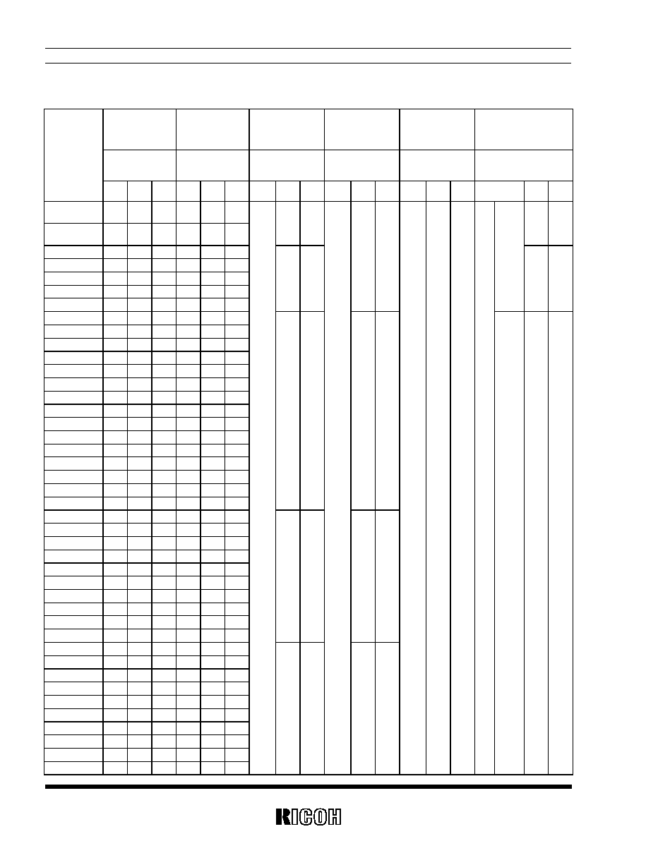
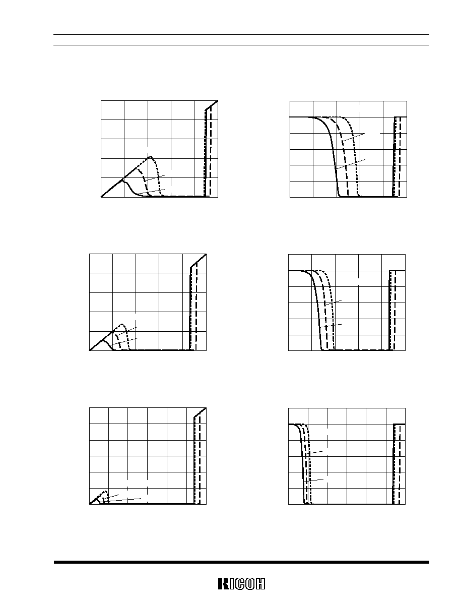
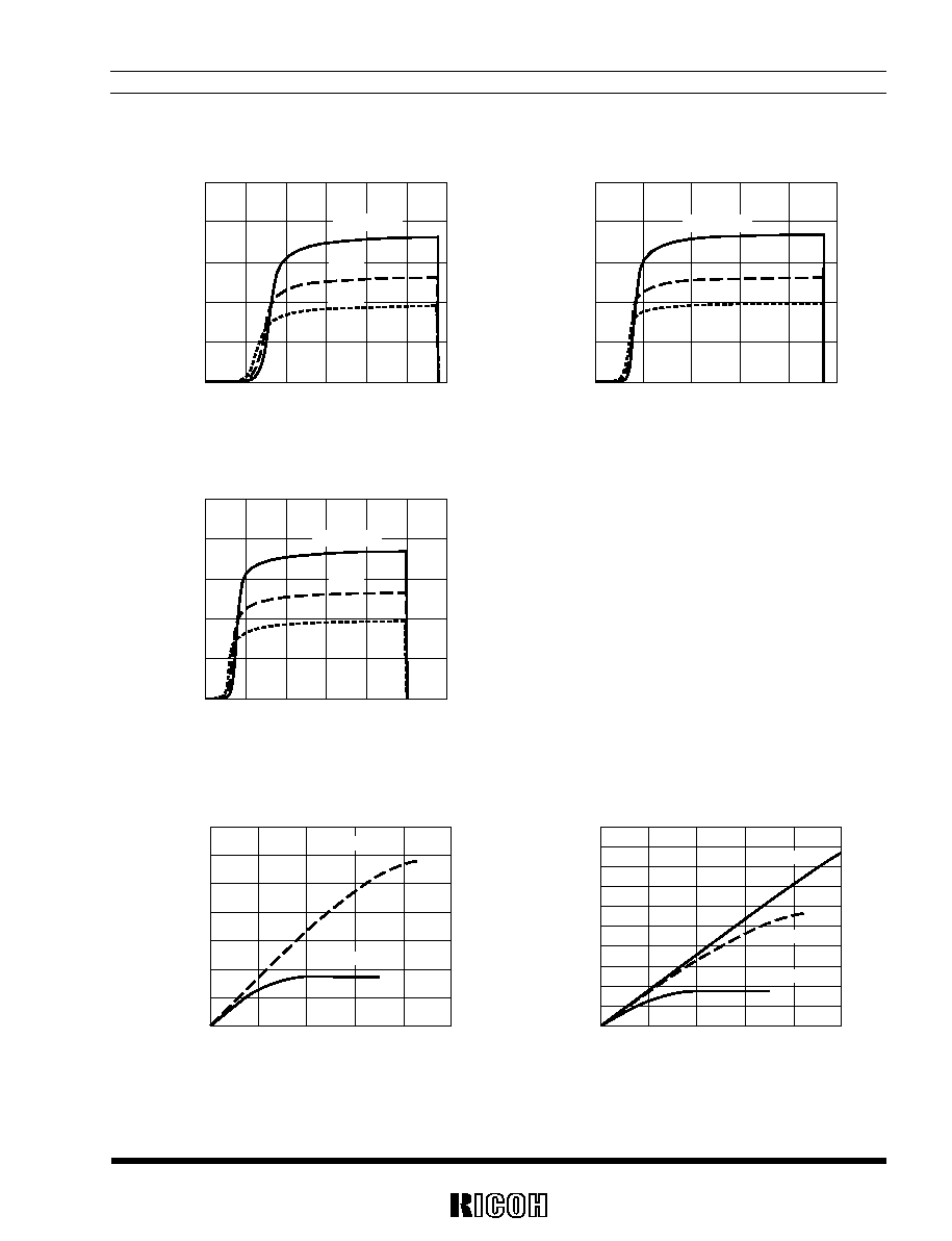
1)
Supply Current vs. Input Voltage
R3115Z091x
R3115Z131x
1.5
0.9
1.2
0.6
0.3
0
Input Voltage V
IN
(V)
Supply Current I
SS
(
µ
A)
0
1
5
7
6
4
3
2
Topt=85
∞C
25
∞C
-40
∞C
1.5
0.9
1.2
0.6
0.3
0
Input Voltage V
IN
(V)
Supply Current I
SS
(
µ
A)
0
1
5
7
6
4
3
2
Topt=85
∞C
25
∞C
-40
∞C
R3115Z271x
R3115Z451x
1.5
0.9
1.2
0.6
0.3
0
Input Voltage V
IN
(V)
Supply Current I
SS
(
µ
A)
0
1
5
7
6
4
3
2
Topt=85
∞C
25
∞C
-40
∞C
2.0
1.2
1.6
0.8
0.4
0
Input Voltage V
IN
(V)
Supply Current I
SS
(
µ
A)
0
1
5
7
6
4
3
2
Topt=85
∞C
25
∞C
-40
∞C
R3115Z501x
2.4
1.6
2.0
1.2
0.8
0.4
0
Input Voltage V
IN
(V)
Supply Current I
SS
(
µ
A)
0
1
5
7
6
4
3
2
Topt=85
∞C
25
∞C
-40
∞C
R3115Z
12
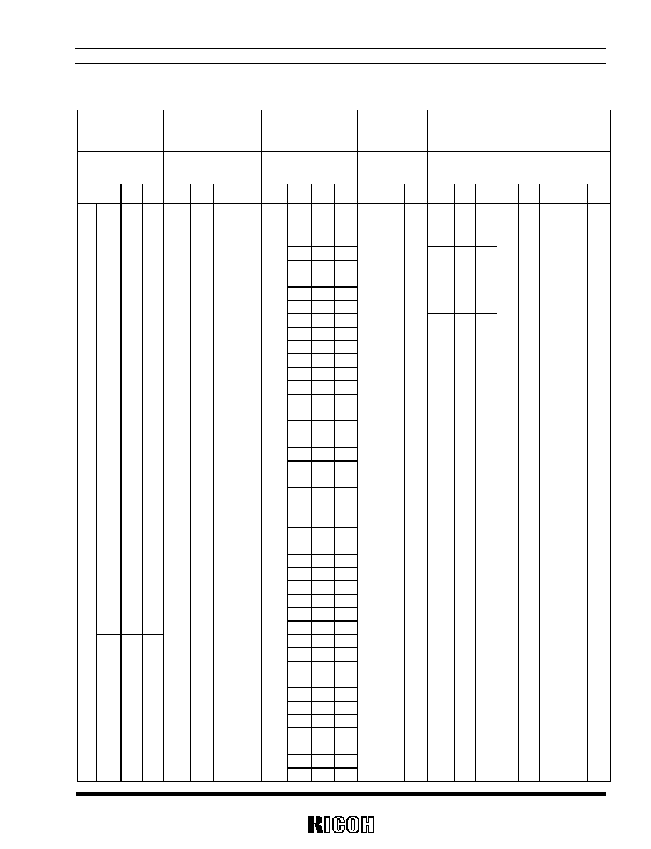
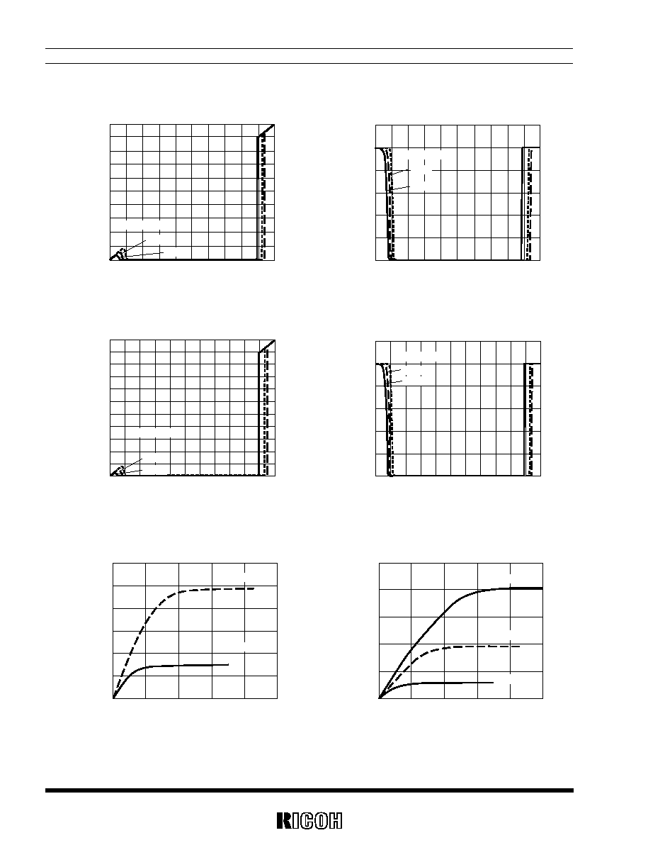
2)
Detector Threshold vs. Temperature
R3115Z091x
R3115Z131x
0.98
0.94
0.96
0.92
0.90
0.88
0.86
Temperature Topt(
∞C)
Detector Threshold/Released Voltage
V
DET
(V)
-50
-25
100
75
50
25
0
-V
DET
+V
DET
1.42
1.36
1.40
1.34
1.30
1.28
1.26
Temperature Topt(
∞C)
Detector Threshold/Released Voltage
V
DET
(V)
-50
-25
100
75
50
25
0
1.32
1.38
-V
DET
+V
DET
R3115Z271x
R3115Z451x
2.90
2.80
2.85
2.75
2.70
2.65
2.60
Temperature Topt(
∞C)
Detector Threshold/Released Voltage
V
DET
(V)
-50
-25
100
75
50
25
0
-V
DET
+V
DET
4.75
4.60
4.70
4.55
4.45
4.40
4.35
Temperature Topt(
∞C)
Detector Threshold/Released Voltage
V
DET
(V)
-50
-25
100
75
50
25
0
4.50
4.65
-V
DET
+V
DET
R3115Z501x
5.30
5.15
5.25
5.10
5.00
4.95
4.90
Temperature Topt(
∞C)
Detector Threshold/Released Voltage
V
DET
(V)
-50
-25
100
75
50
25
0
5.05
5.20
-V
DET
+V
DET
R3115Z
13
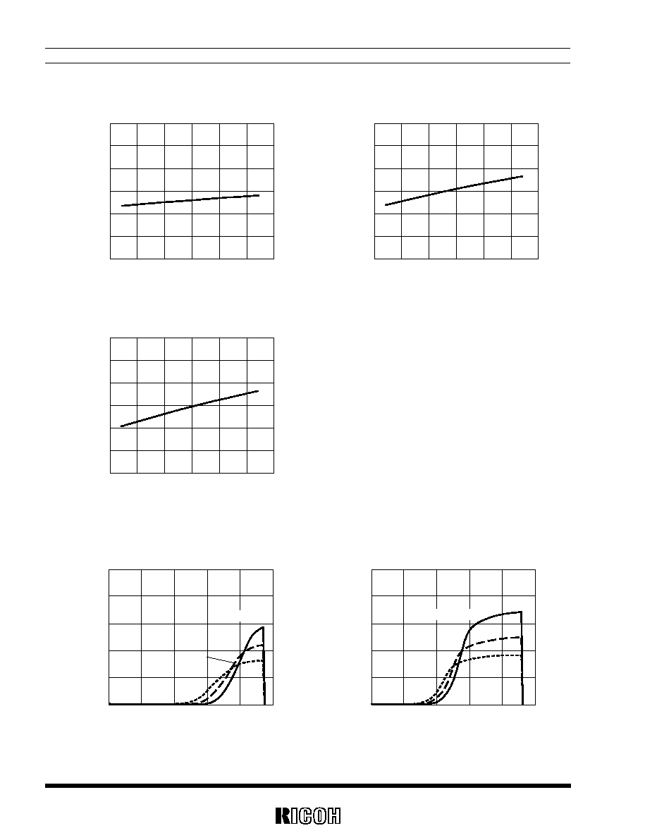
3)
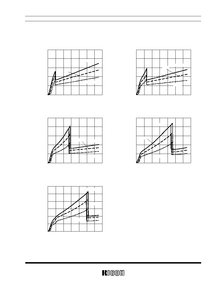
Output Voltage vs. Input Voltage
R3115Z091x
R3115Z091A
1.0
0.8
0.6
0.2
0.0
Input Voltage V
IN
(V)
Output Voltage V
OUT
(V)
0
0.2
0.4
0.6
0.8
1
0.4
Nch Output Type: V
DD
pull up
Topt=-40
∞C
25
∞C
85
∞C
6.0
5.0
0.0
Input Voltage V
IN
(V)
Output Voltage V
OUT
(V)
0
0.2
0.4
0.6
0.8
1
4.0
3.0
2.0
1.0
5V pull up via 470k
Topt=-40
∞C
25
∞C
85
∞C
R3115Z131x
R3115Z131A
1.5
1.2
0.9
0.3
0
Input Voltage V
IN
(V)
Output Voltage V
OUT
(V)
0
0.3
0.6
0.9
1.2
1.5
0.6
Nch Output Type: V
DD
pull up
Topt=-40
∞C
25
∞C
85
∞C
6.0
5.0
0.0
Input Voltage V
IN
(V)
Output Voltage V
OUT
(V)
0
0.3
0.6
0.9
1.2
1.5
4.0
3.0
2.0
1.0
5V pull up via 470k
Topt=-40
∞C
25
∞C
85
∞C
R3115Z271x
R3115Z271A
3.0
2.5
2.0
0.5
0.0
Input Voltage V
IN
(V)
Output Voltage V
OUT
(V)
0.0
0.5
1.5
2.0
2.5
3.0
1.0
1.5
1.0
Nch Output Type: V
DD
pull up
Topt=-40
∞C
25
∞C
85
∞C
6.0
5.0
0.0
Input Voltage V
IN
(V)
Output Voltage V
OUT
(V)
0.0
0.5
1.5
2.0
2.5
3.0
4.0
3.0
2.0
1.0
1.0
5V pull up via 470k
Topt=-40
∞C
25
∞C
85
∞C
R3115Z
14
R3115Z451x
R3115Z451A
5.0
4.0
3.5
0.5
0.0
Input Voltage V
IN
(V)
Output Voltage V
OUT
(V)
0.0
1.0
2.5
4.0 4.5 5.0
1.5
1.0
3.0
2.5
2.0
4.5
0.5
3.0
1.5 2.0
3.5
Nch Output Type: V
DD
pull up
Topt=-40
∞C
25
∞C
85
∞C
6.0
5.0
0.0
Input Voltage V
IN
(V)
Output Voltage V
OUT
(V)
0.0 0.5
2.5 3.0
5.0
4.0
3.0
2.0
1.0
1.5 2.0
1.0
3.5 4.0 4.5
5V pull up via 470k
Topt=-40
∞C
25
∞C
85
∞C
R3115Z501x
R3115Z501A
5.5
5.0
4.0
3.5
0.5
0.0
Input Voltage V
IN
(V)
Output Voltage V
OUT
(V)
0.0
1.0
2.5
4.0 4.5
5.5
5.0
1.5
1.0
3.0
2.5
2.0
4.5
0.5
3.0
1.5 2.0
3.5
Nch Output Type: V
DD
pull up
Topt=-40
∞C
25
∞C
85
∞C
6.0
5.0
0.0
Input Voltage V
IN
(V)
Output Voltage V
OUT
(V)
0.0 0.5 1.0 1.5 2.0 2.5 3.0 3.5 4.0 4.5 5.0 5.5
4.0
3.0
2.0
1.0
5V pull up via 470k
Topt=-40
∞C
25
∞C
85
∞C
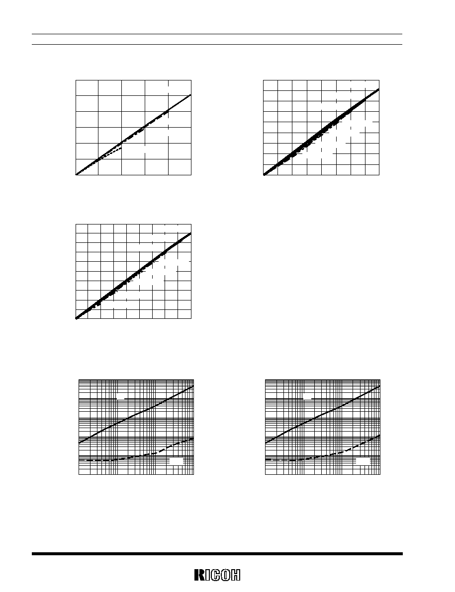
4)
Nch Driver Output Current vs. V
DS
R3115Z091x
R3115Z131x
1.2
1.0
0.2
0.4
0.6
0.8
0
V
DS
(V)
Output Current I
OUT
(mA)
0
0.2
0.4
0.6
0.8
1
V
DD
=0.85V
V
DD
=0.7V
2.5
2.0
1.5
1.0
0.5
0
V
DS
(V)
Output Current I
OUT
(mA)
0
0.2
0.4
0.6
0.8
1
V
DD
=1.0V
V
DD
=0.85V
V
DD
=0.7V

R3115Z
15
R3115Z271x
R3115Z451x
20
16
12
8
4
0
V
DS
(V)
Output Current I
OUT
(mA)
0
0.5
1
1.5
2
2.5
V
DD
=2.5V
V
DD
=2.0V
V
DD
=1.5V
V
DD
=1.0V
20
16
12
8
4
0
V
DS
(V)
Output Current I
OUT
(mA)
0
0.5
1
1.5
2
3.5
3
2.5
4
V
DD
=2.5V
V
DD
=3.5V
V
DD
=4.0V
V
DD
=3.0V
V
DD
=2.0V
V
DD
=1.5V
V
DD
=1.0V
R3115Z501x
20
16
12
8
4
0
V
DS
(V)
Output Current I
OUT
(mA)
0
1
0.5
2
1.5
3
2.5
4
3.5
4.5
V
DD
=2.5V
V
DD
=3.5V
V
DD
=4.0V
V
DD
=4.5V
V
DD
=3.0V
V
DD
=2.0V
V
DD
=1.5V
V
DD
=1.0V
5)
Nch Driver Output Current vs. Input Voltage
R3115Z091x
R3115Z131x
2.0
1.5
1.0
0.5
0.0
Input Voltage V
IN
(V)
Output Current I
OUT
(mA)
0
0.2
0.8
1
0.4
0.6
Topt=85
∞C
-40
∞C
25
∞C
5
4
3
2
0
Input Voltage V
IN
(V)
Output Current I
OUT
(mA)
0
0.3
1.2
1.5
1
0.6
0.9
Topt=85
∞C
-40
∞C
25
∞C

R3115Z
16
R3115Z271x
R3115Z451x
5
4
3
2
0
Input Voltage V
IN
(V)
Output Current I
OUT
(mA)
0
3
1
1.5
0.5
1
2
2.5
Topt=85
∞C
-40
∞C
25
∞C
5
4
3
2
0
Input Voltage V
IN
(V)
Output Current I
OUT
(mA)
0
5
1
2
1
3
4
Topt=85
∞C
-40
∞C
25
∞C
R3115Z501x
7
0
Input Voltage V
IN
(V)
Output Current I
OUT
(mA)
0
6
1
6
5
4
3
2
1
2
3
4
5
Topt=85
∞C
-40
∞C
25
∞C
6)
Pch Driver Output Current vs. Input Voltage
R3115Z091C
R3115Z131C
0
Input Voltage V
IN
(V)
Output Current I
OUT
(mA)
0
7
1
6
5
4
3
2
1
2
3
5
6
4
V
DS
=-2.1V
-1.5V
-1.0V
-0.5V
0
Input Voltage V
IN
(V)
Output Current I
OUT
(mA)
0
7
1
6
5
4
3
2
1
2
3
5
6
4
V
DS
=-2.1V
-1.5V
-1.0V
-0.5V
R3115Z
17
R3115Z271C
R3115Z451C
0
Input Voltage V
IN
(V)
Output Current I
OUT
(mA)
0
7
1
6
5
4
3
2
1
2
3
5
6
4
V
DS
=-2.1V
-1.5V
-1.0V
-0.5V
0
Input Voltage V
IN
(V)
Output Current I
OUT
(mA)
0
7
1
6
5
4
3
2
1
2
3
5
6
4
V
DS
=-2.1V
-1.5V
-1.0V
-0.5V
R3115Z501C
0
Input Voltage V
IN
(V)
Output Current I
OUT
(mA)
0
7
1
6
5
4
3
2
1
2
3
5
6
4
V
DS
=-2.1V
-1.5V
-1.0V
-0.5V
7)
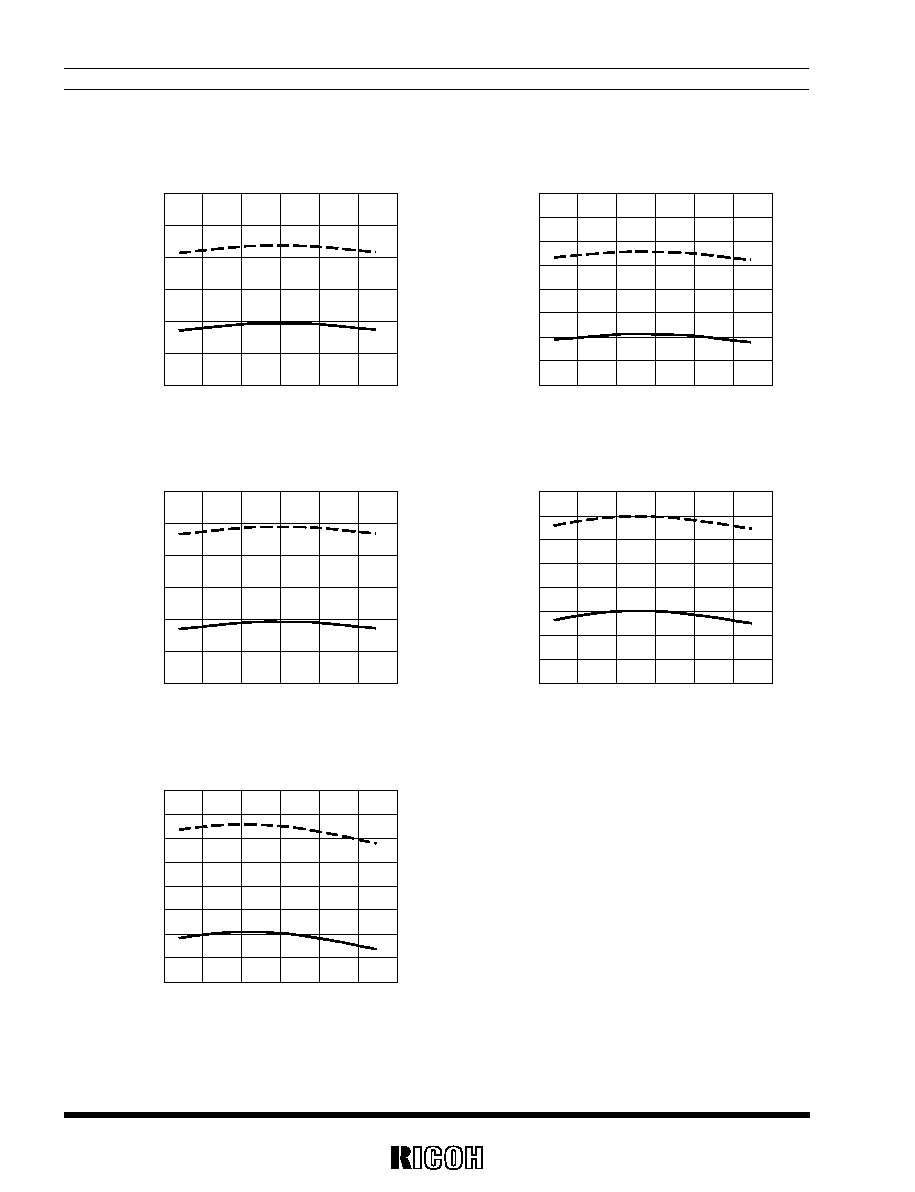
C
D
Pin Threshold Voltage vs. Temperature
R3115Z091x
R3115Z131x
0.8
0.6
0.7
0.5
0.4
0.3
0.2
-50
-25
100
75
50
25
0
Temperature Topt(
∞C)
C
D
Pin Threshold Voltage V
TCD
(V)
V
DD
=0.99V
1.0
0.8
0.9
0.7
0.6
0.5
0.4
-50
-25
100
75
50
25
0
Temperature Topt(
∞C)
C
D
Pin Threshold Voltage V
TCD
(V)
V
DD
=1.43V
R3115Z
18
R3115Z271x
R3115Z451x
1.9
1.7
1.8
1.6
1.5
1.4
1.3
-50
-25
100
75
50
25
0
Temperature Topt(
∞C)
C
D
Pin Threshold Voltage V
TCD
(V)
V
DD
=2.97V
2.9
2.7
2.8
2.6
2.5
2.4
2.3
-50
-25
100
75
50
25
0
Temperature Topt(
∞C)
C
D
Pin Threshold Voltage V
TCD
(V)
V
DD
=4.95V
R3115Z501x
3.2
3.0
3.1
2.9
2.8
2.7
2.6
Temperature Topt(
∞C)
C
D
Pin Threshold Voltage V
TCD
(V)
-50
-25
100
75
50
25
0
V
DD
=5.50V
8)
C
D
Pin Output Current vs. Input Voltage
R3115Z091x
R3115Z131x
1.0
0.8
0.6
0.4
0
Input Voltage V
IN
(V)
0
0.2
0.8
1
0.2
0.4
0.6
C
D
Pin Output Current I
CD
(mA)
V
DS
=0.5V
Topt=-40
∞C
85
∞C
25
∞C
1.0
0.8
0.6
0.4
0
Input Voltage V
IN
(V)
0
0.3
1.2
1.5
0.2
0.6
0.9
C
D
Pin Output Current I
CD
(mA)
V
DS
=0.5V
Topt=-40
∞C
85
∞C
25
∞C
R3115Z
19
R3115Z271x
R3115Z451x
1.0
0.8
0.6
0.4
0
Input Voltage V
IN
(V)
0
0.5
3
2
1
0.2
2.5
1.5
C
D
Pin Output Current I
CD
(mA)
V
DS
=0.5V
Topt=-40
∞C
85
∞C
25
∞C
1.0
0.8
0.6
0.4
0
Input Voltage V
IN
(V)
0
1
4
5
0.2
2
3
C
D
Pin Output Current I
CD
(mA)
V
DS
=0.5V
Topt=-40
∞C
85
∞C
25
∞C
R3115Z501x
1.0
0.8
0.6
0.4
0
Input Voltage V
IN
(V)
C
D
Pin Output Current I
CD
(mA)
0
1
6
4
2
0.2
5
3
V
DS
=0.5V
Topt=-40
∞C
85
∞C
25
∞C
9)
C
D
Pin Output Current vs. V
DS
(Topt=25∞C)
R3115Z091x
R3115Z131x
0.7
0.6
0.5
0.1
0.2
0.3
0.4
0
V
DS
(V)
C
D
Pin Output Current I
CD
(mA)
0
0.2
0.4
0.6
0.8
1
V
DD
=0.85V
V
DD
=0.7V
1.0
0.9
0.8
0.7
0.6
0.5
0.4
0.3
0.2
0.1
0
V
DS
(V)
C
D
Pin Output Current I
CD
(mA)
0
0.2
0.4
0.6
0.8
1
V
DD
=1.0V
V
DD
=0.85V
V
DD
=0.7V
R3115Z
20
R3115Z271x
R3115Z451x
3.0
2.5
2.0
1.5
1.0
0.5
0
V
DS
(V)
C
D
Pin Output Current I
CD
(mA)
0
0.5
1
1.5
2
2.5
V
DD
=2.5V
V
DD
=2.0V
V
DD
=1.5V
V
DD
=1.0V
4.5
0
0.5
1.0
1.5
2.0
2.5
3.0
3.5
4.0
V
DS
(V)
C
D
Pin Output Current I
CD
(mA)
0
0.5
1
1.5
2
3.5
3
2.5
4
V
DD
=2.5V
V
DD
=3.5V
V
DD
=4.0V
V
DD
=3.0V
V
DD
=2.0V
V
DD
=1.5V
V
DD
=1.0V
R3115Z501x
5.0
4.0
3.0
2.0
1.0
0
V
DS
(V)
C
D
Pin Output Current I
CD
(mA)
0
1
0.5
2
1.5
3
2.5
4
3.5
4.5
0.5
2.5
1.5
4.5
3.5
V
DD
=2.5V
V
DD
=3.5V
V
DD
=4.0V
V
DD
=4.5V
V
DD
=3.0V
V
DD
=2.0V
V
DD
=1.5V
V
DD
=1.0V
10) Output Delay Time vs. External Capacitance (Topt=25∞C)
R3115Z091x
R3115Z131x
1000
100
10
1
0.1
0.01
External Capacitance C
D
(
µF)
Output Delay Time tx(ms)
0.0001
0.001
0.01
0.1
t
PHL
t
D
1000
100
10
1
0.1
0.01
External Capacitance C
D
(
µF)
Output Delay Time t
D
(ms)
0.0001
0.001
0.01
0.1
t
PHL
t
D

R3115Z
21
R3115Z271x
R3115Z451x
1000
100
10
1
0.1
0.01
External Capacitance C
D
(
µF)
Output Delay Time tx(ms)
0.0001
0.001
0.01
0.1
t
PHL
t
D
1000
100
10
1
0.1
0.01
External Capacitance C
D
(
µF)
Output Delay Time tx(ms)
0.0001
0.001
0.01
0.1
t
PHL
t
D
R3115Z501x
1000
100
10
1
0.1
0.01
External Capacitance C
D
(
µF)
Output Delay Time tp(ms)
0.0001
0.001
0.01
0.1
t
PHL
t
D
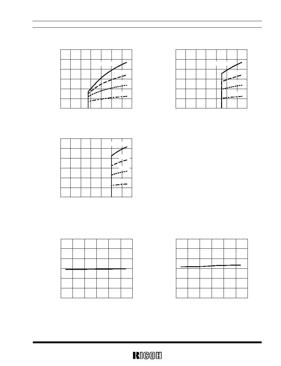
11) Delay Circuit Resistance vs. Temperature
R3115Zxx1x
13
12
11
10
9
8
7
6
5
4
3
Temperature Topt(
∞C)
Delay Circuit Resistance R
D
(M
)
-50
-25
0
25
50
75
100
R3115Z
22
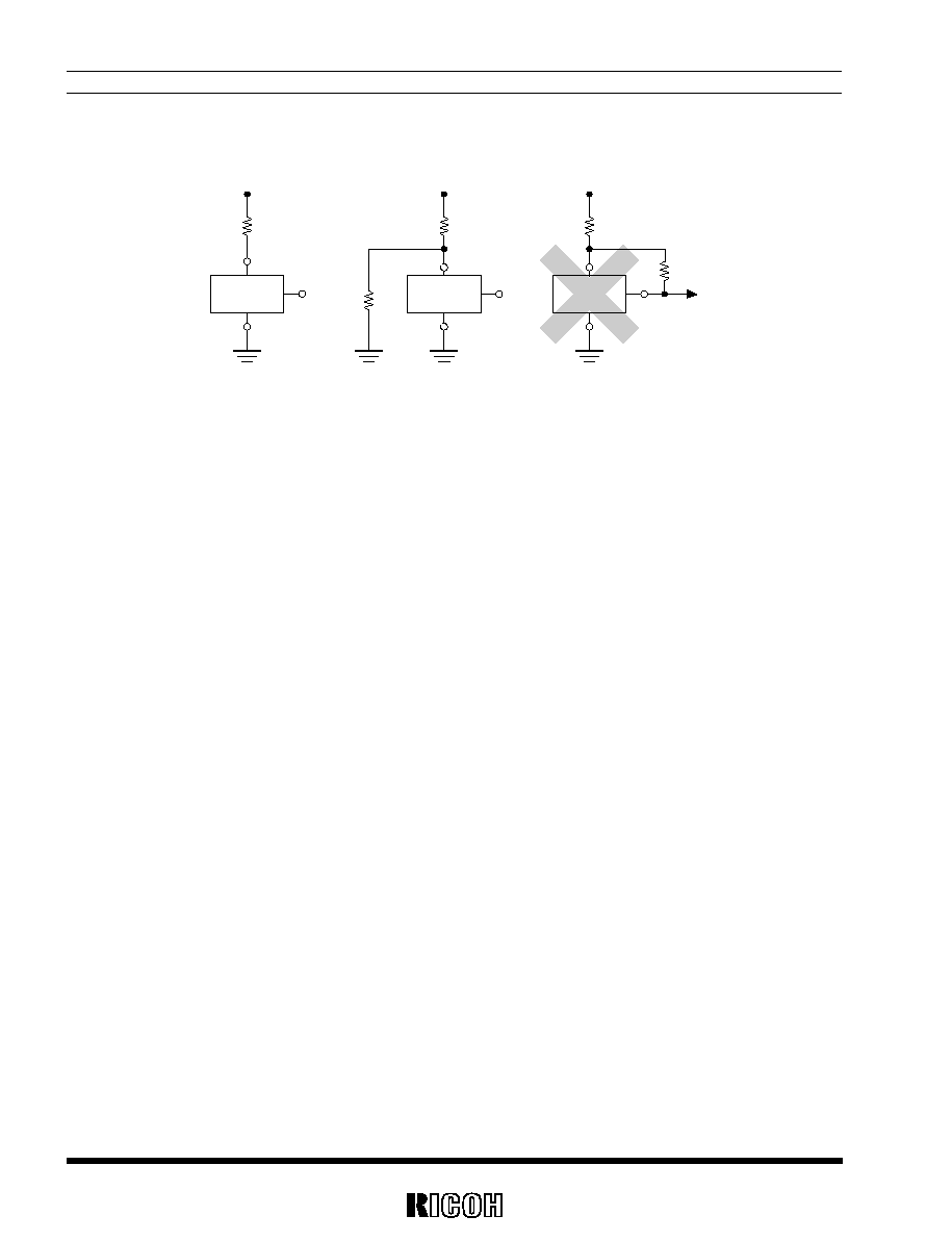
TECHNICAL NOTES
R
V
DD
GND
OUT
R3115Z
Series
V
DD
R1
R2
V
DD
GND
OUT
V
DD
R1
R2
V
DD
GND
OUT
R3115Z
Series
R3115Z
Series
Figure A
Figure B
Figure C
When R3115Zxx1A (Nch Open Drain Output Type) is used in Figure A or Figure B, if Impedance of Voltage Supply
pIn, V
DD
and V
DD
of this IC is large, detector threshold level would shift by voltage dropdown caused by the consump-
tion current of the IC itself. Released voltage may also shift and delay time for start-up might be generated by this us-
age.
When R3115Zxx1C (CMOS Output Type) is used in Figure A or Figure B, Output level could be unstable by cross
conduction current which is generated at detector threshold level or at released voltage level, therefore, do not use
R3115Zxx1C with the connection in Figure A or Figure B.
The connection in Figure C may cause the oscillation in both R3115Zxx1C (CMOS Output) and R3115Zxx1A (Nch
Open Drain Output), therefore do not use R3115Zxx1x Series with the connection in Figure C.