'98.Dec.05
LOW VOLTAGE DETECTOR
R3111xxx1A/C Series
Rev.1.10
- 1 -
s
OUTLINE
The R3111 Series are voltage detector ICs with high detector threshold accuracy and ultra-low supply current by CMOS
process, which can be operated at an extremely low voltage and is used for system reset as an example.
Each of these ICs consists of a voltage reference unit, a comparator, resistors for detector threshold setting, an output driver
and a hysteresis circuit. The detector threshold is fixed with high accuracy internally and does not require any adjustment.
Two output types, Nch open drain type and CMOS type are available.
The R3111 Series are operable at a lower voltage than that for the RX5VL Series, and can be driven by a single battery.
Four types of packages, TO-92, SOT-89, SOT-23-5 and SC-82AB are available.
s
FEATURES
q
Ultra-low Supply Current ............................................................... TYP. 0.8µA (V
DD
=1.5V)
q
Wide Range of Operating Voltage .................................................. 0.7 to 10.0V(Topt=25
∞
C)
q
Detector Threshold ......................................................................... Stepwise setting with a step of 0.1V in the range of
0.9V to 6.0V is possible.
q
High Accuracy Detector Threshold................................................ ±2.0%
q
Low Temperature-Drift Coefficient of Detector Threshold............ TYP. ±100ppm/
∞
C
q
Two Output Types .......................................................................... Nch Open Drain and CMOS
q
Four Types of Packages.................................................................. TO-92, SOT-89(Mini-power Mold), SOT-23-5 (Mini-
mold), SC-82AB
s
APPLICATIONS
q
CPU and Logic Circuit Reset
q
Battery Checker
q
Window Comparator
q
Wave Shaping Circuit
q
Battery Back-up Circuit
q
Power Failure Detector
s
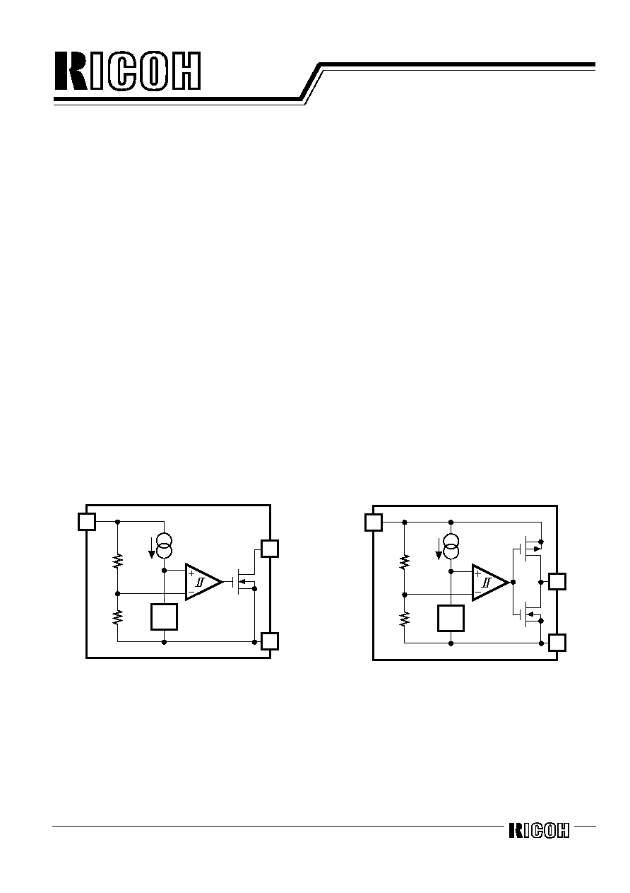
BLOCK DIAGRAMS
R3111XXX1A
R3111XXX1C
V
DD
OUT
GND
Vref
V
DD
OUT
GND
Vref
Rev.1.10
- 2 -
s
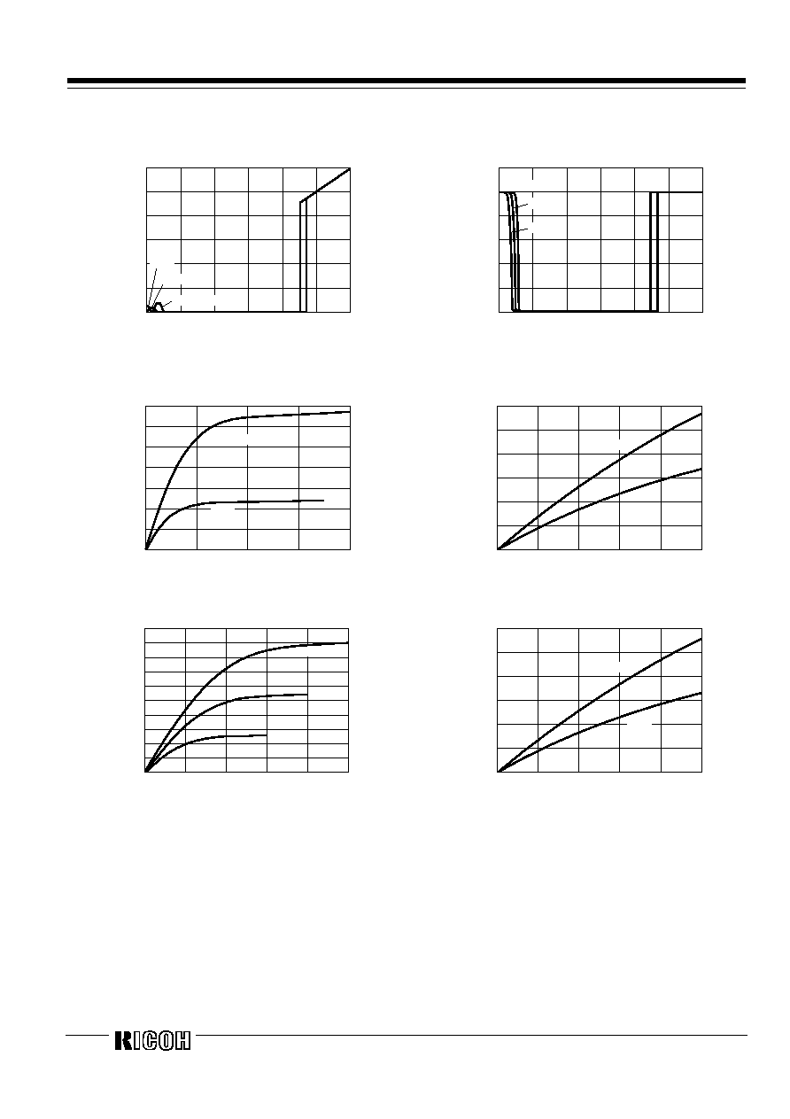
TIMING CHART
t
PLH
Supply Voltage
Output Voltage
(OUT)
Minimum Operating Voltage
V
SS
V
SS
Detector Threshold
Hysteresis
(V
DD
)
Release Voltage +V
DET
Detector Threshold -V
DET
s
DEFINITION OF OUTPUT DELAY TIME
Output Delay Time t
PLH
is defined as follows:
1.
In the case of Nch Open Drain Output:
Under the condition of the output pin (OUT) is pulled up through a resistor of 470k
to 5V, the time interval between the
rising edge of V
DD
pulse from 0.7V to (+V
DET
)+ 2.0V and becoming of the output voltage to 2.5V.
2.
In the case of CMOS Output:
The time interval between the rising edge of V
DD
pulse from 0.7V to (+V
DET
)+ 2.0V and becoming of the output voltage to
(V
DD
/
2) V.
+V
DET
+ 2.0V
5.0V
2.5V
0.7V
Input Voltage
(V
DD
)
Output Voltage
GND
GND
t
PHL
t
PLH
+V
DET
+ 2.0V
+V
DET
+2.0V
+V
DET
+2.0V
0.7V
Input Voltage
(V
DD
)
Output Voltage
GND
2
GND
t
PHL
t
PLH
Nch Open Drain Output
CMOS Output
Rev.1.10
- 3 -
s
SELECTION GUIDE
The package type, the detector threshold, the output type and the taping type of R3111 Series can be designated at the users'
request by specifying the part number as follows;
R3111
◊◊◊
1
◊
-
◊◊
Part Number
a b c d
Code
Contents
a
Designation of Package Type;
E: TO-92
Q: SC-82AB
H: SOT-89
N: SOT-23-5
b
Setting Detector Threshold (-V
DET
);
Stepwise setting with a step of 0.1V in the range of 0.9V to 6.0V is possible.
c
Designation of Output Type;
A: Nch Open Drain
C: CMOS
d
Designation of Packing or Taping Type ;
Ex.TO-92: TZ, SOT-89: T1,
SOT-23-5, SC-82AB: TR are prescribed as standard directions.
(Refer to Taping Specifications.) Antistatic bag for samples: C
Rev.1.10
- 4 -
s
PIN CONFIGURATION
q
TO-92
q
SOT-89
q
SOT-23-5
q
SC-82AB
1
2
3
(mark side)
1
2
3
(mark side)
1
2
3
5
4
(mark side)
4
3
1
2
(mark side)
s
PIN DESCRIPTION
q
TO-92
q
SOT-89
q
SOT-23-5
q
SC-2AB
Pin No.
Symbol
Pin No.
Symbol
Pin No.
Symbol
Pin No.
Symbol
1
V
DD
1
OUT
1
OUT
1
OUT
2
GND
2
V
DD
2
V
DD
2
V
DD
3
OUT
3
GND
3
GND
3
NC
4
NC
4
GND
5
NC
s
ABSOLUTE MAXIMUM RATINGS
Symbol
Item
Rating
Unit
V
DD
Supply Voltage
12
V
V
OUT1
Output Voltage (CMOS)
V
SS
-0.3 to V
DD
+0.3
V
V
OUT2
Output Voltage (Nch)
V
SS
-0.3 to 12
V
I
OUT
Output Current
70
mA
P
D
Power Dissipation 1*
Note1
300
mW
P
D
Power Dissipation 2*
Note2
150
mW
Topt
Operating Temperature
Range
-40 to 85
∞
C
Tstg
Storage Temperature
Range
-55 to 125
∞
C
Tsolder
Lead temperature
(Soldering)
260
∞
C, 10s
*Note 1: applied to SOT-89 and TO-92
*Note 2: applied to SOT-23-5 and SC-82AB
Rev.1.10
- 5 -
s
ELECTRICAL CHARACTERISTICS
q
R3111x091A/C
Topt=25
∞
C
Symbol
Item
Conditions
MIN.
TYP.
MAX.
Unit
-V
DET
Detector Threshold
0.882
0.900
0.918
V
V
HYS
Detector Threshold Hysteresis
0.027
0.045
0.063
V
I
SS
Supply Current
V
DD
=0.80V
2.90V
0.8
0.9
2.4
2.7
µ
A
V
DDH
Maximum Operating Voltage
10
V
Topt=25
∞
C
0.55
0.70
V
DDL
Minimum Operating
Voltage*
Note1
-40
∞
C
Topt
85
∞
C
0.65
0.80
V
Nch
V
DS
=0.05V,V
DD
=0.70V
V
DS
=0.50V,V
DD
=0.85V
0.01
0.05
0.05
0.50
mA
I
OUT
Output Current
(Driver Output Pin)
Pch
V
DS
=-2.1V,V
DD
=4.5V
1.0
2.0
mA
t
PLH
Output Delay Time*
Note2
100
µ
s
-V
DET
/
T
Detector Threshold Temperature
Coefficient
-40
∞
C
Topt
85
∞
C
±
100
ppm/
∞
C
q
R3111x181A/C
Topt=25
∞
C
Symbol
Item
Conditions
MIN.
TYP.
MAX.
Unit
-V
DET
Detector Threshold
1.764
1.800
1.836
V
V
HYS
Detector Threshold Hysteresis
0.054
0.090
0.126
V
I
SS
Supply Current
V
DD
=1.70V
3.80V
0.8
1.0
2.4
3.0
µ
A
V
DDH
Maximum Operating Voltage
10
V
Topt=25
∞
C
0.55
0.70
V
DDL
Minimum Operating
Voltage*
Note1
-40
∞
C
Topt
85
∞
C
0.65
0.80
V
Nch
V
DS
=0.05V,V
DD
=0.70V
V
DS
=0.50V,V
DD
=0.85V
0.01
1.00
0.05
2.00
mA
I
OUT
Output Current
(Driver Output Pin)
Pch
V
DS
=-2.1V,V
DD
=4.5V
1.0
2.0
mA
t
PLH
Output Delay Time*
Note2
100
µ
s
-V
DET
/
T
Detector Threshold Temperature
Coefficient
-40
∞
C
Topt
85
∞
C
±
100
ppm/
∞
C
Rev.1.10
- 6 -
q
R3111x271A/C
Topt=25
∞
C
Symbol
Item
Conditions
MIN.
TYP.
MAX.
Unit
-V
DET
Detector Threshold
2.646
2.700
2.754
V
V
HYS
Detector Threshold Hysteresis
0.081
0.135
0.189
V
I
SS
Supply Current
V
DD
=2.60V
4.70V
0.9
1.1
2.7
3.3
µ
A
V
DDH
Maximum Operating Voltage
10
V
Topt=25
∞
C
0.55
0.70
V
DDL
Minimum Operating
Voltage*
Note1
-40
∞
C
Topt
85
∞
C
0.65
0.80
V
Nch
V
DS
=0.05V,V
DD
=0.70V
V
DS
=0.50V,V
DD
=1.50V
0.01
1.00
0.05
2.00
mA
I
OUT
Output Current
(Driver Output Pin)
Pch
V
DS
=-2.1V,V
DD
=4.5V
1.0
2.0
mA
t
PLH
Output Delay Time*
Note2
100
µ
s
-V
DET
/
T
Detector Threshold Temperature
Coefficient
-40
∞
C
Topt
85
∞
C
±
100
ppm/
∞
C
q
R3111x361A/C
Topt=25
∞
C
Symbol
Item
Conditions
MIN.
TYP.
MAX.
Unit
-V
DET
Detector Threshold
3.528
3.600
3.672
V
V
HYS
Detector Threshold Hysteresis
0.108
0.180
0.252
V
I
SS
Supply Current
V
DD
=3.47V
5.60V
1.0
1.2
3.0
3.6
µ
A
V
DDH
Maximum Operating Voltage
10
V
Topt=25
∞
C
0.55
0.70
V
DDL
Minimum Operating
Voltage*
Note1
-40
∞
C
Topt
85
∞
C
0.65
0.80
V
Nch
V
DS
=0.05V,V
DD
=0.70V
V
DS
=0.50V,V
DD
=1.50V
0.01
1.00
0.05
2.00
mA
I
OUT
Output Current
(Driver Output Pin)
Pch
V
DS
=-2.1V,V
DD
=4.5V
1.0
2.0
mA
t
PLH
Output Delay Time*
Note2
100
µ
s
-V
DET
/
T
Detector Threshold Temperature
Coefficient
-40
∞
C
Topt
85
∞
C
±
100
ppm/
∞
C
Rev.1.10
- 7 -
q
R3111x451A/C
Topt=25
∞
C
Symbol
Item
Conditions
MIN.
TYP.
MAX.
Unit
-V
DET
Detector Threshold
4.410
4.500
4.590
V
V
HYS
Detector Threshold Hysteresis
0.135
0.225
0.315
V
I
SS
Supply Current
V
DD
=4.34V
6.50V
1.1
1.3
3.3
3.9
µ
A
V
DDH
Maximum Operating Voltage
10
V
Topt=25
∞
C
0.55
0.70
V
DDL
Minimum Operating
Voltage*
Note1
-40
∞
C
Topt
85
∞
C
0.65
0.80
V
Nch
V
DS
=0.05V,V
DD
=0.70V
V
DS
=0.50V,V
DD
=1.50V
0.01
1.00
0.05
2.00
mA
I
OUT
Output Current
(Driver Output Pin)
Pch
V
DS
=-2.1V,V
DD
=8.0V
1.5
3.0
mA
t
PLH
Output Delay Time*
Note2
100
µ
s
-V
DET
/
T
Detector Threshold Temperature
Coefficient
-40
∞
C
Topt
85
∞
C
±
100
ppm/
∞
C
q
R3111x541A/C
Topt=25
∞
C
Symbol
Item
Conditions
MIN.
TYP.
MAX.
Unit
-V
DET
Detector Threshold
5.292
5.400
5.508
V
V
HYS
Detector Threshold Hysteresis
0.162
0.270
0.378
V
I
SS
Supply Current
V
DD
=5.20V
7.40V
1.2
1.4
3.6
4.2
µ
A
V
DDH
Maximum Operating Voltage
10
V
Topt=25
∞
C
0.55
0.70
V
DDL
Minimum Operating
Voltage*
Note1
-40
∞
C
Topt
85
∞
C
0.65
0.80
V
Nch
V
DS
=0.05V,V
DD
=0.70V
V
DS
=0.50V,V
DD
=1.50V
0.01
1.00
0.05
2.00
mA
I
OUT
Output Current
(Driver Output Pin)
Pch
V
DS
=-2.1V,V
DD
=8.0V
1.5
3.0
mA
t
PLH
Output Delay Time*
Note2
100
µ
s
-V
DET
/
T
Detector Threshold Temperature
Coefficient
-40
∞
C
Topt
85
∞
C
±
100
ppm/
∞
C
*Note1: Minimum Operating Voltage means the value of input voltage when output voltage maintains 0.1V or less.
(In the case of Nch Open Drain Type, Output pin is pulled up with a resistance of 470k
to 5.0V.)
*Note2: In the case of CMOS Output Type: The time interval between the rising edge of V
DD
input pulse from
0.7V to
(+V
DET
)+2.0V and output voltage level becoming to V
DD
/2.
In the case of Nch Open Drain Output Type: Output pin is pulled up with a resistance of 470k
to 5.0V, The
time interval between the rising edge of V
DD
input pulse from
0.7V to (+V
DET
)+2.0V and output voltage level
becoming to 2.5V.

Rev.1.10
- 8 -
s
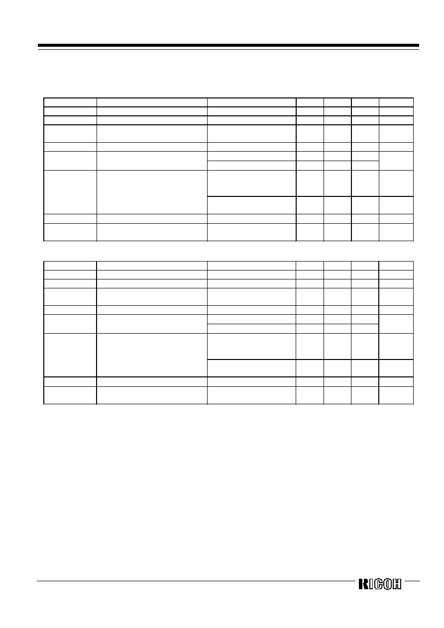
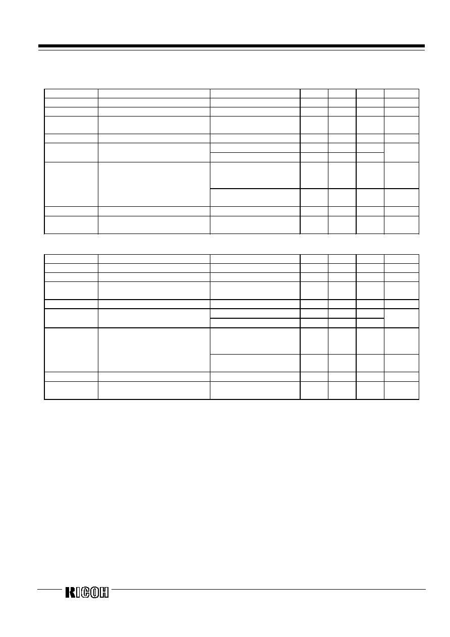
ELECTRICAL CHARACTERISRICS BY DETECTOR THRESHOLD
q
R3111x09x to R3111x60x
Detector Threshold
Detector Threshold
Hysteresis
Supply Current 1
Supply Current 2
Part
Number
-V
DET
[V]
V
HYS
[V]
I
SS1
[
µ
A]
I
SS2
[
µ
A]
MIN.
TYP.
MAX.
MIN.
TYP.
MAX.
Condition
TYP.
MAX.
Condition
TYP.
MAX.
R3111x091x
0.882
0.900
0.918
0.027
0.045
0.063
0.9
2.7
R3111x101x
0.980
1.000
1.020
0.030
0.050
0.070
R3111x111x
1.078
1.100
1.122
0.033
0.055
0.077
R3111x121x
1.176
1.200
1.224
0.036
0.060
0.084
R3111x131x
1.274
1.300
1.326
0.039
0.065
0.091
R3111x141x
1.372
1.400
1.428
0.042
0.070
0.098
R3111x151x
1.470
1.500
1.530
0.045
0.075
0.105
R3111x161x
1.568
1.600
1.632
0.048
0.080
0.112
R3111x171x
1.666
1.700
1.734
0.051
0.085
0.119
R3111x181x
1.764
1.800
1.836
0.054
0.090
0.126
R3111x191x
1.862
1.900
1.938
0.057
0.095
0.133
0.8
2.4
1.0
3.0
R3111x201x
1.960
2.000
2.040
0.060
0.100
0.140
R3111x211x
2.058
2.100
2.142
0.063
0.105
0.147
R3111x221x
2.156
2.200
2.244
0.066
0.110
0.154
R3111x231x
2.254
2.300
2.346
0.069
0.115
0.161
R3111x241x
2.352
2.400
2.448
0.072
0.120
0.168
R3111x251x
2.450
2.500
2.550
0.075
0.125
0.175
R3111x261x
2.548
2.600
2.652
0.078
0.130
0.182
R3111x271x
2.646
2.700
2.754
0.081
0.135
0.189
R3111x281x
2.744
2.800
2.856
0.084
0.140
0.196
R3111x291x
2.842
2.900
2.958
0.087
0.145
0.203
V
DD
=
(-V
DET
)
-0.10V
0.9
2.7
1.1
3.3
R3111x301x
2.940
3.000
3.060
0.090
0.150
0.210
R3111x311x
3.038
3.100
3.162
0.093
0.155
0.217
R3111x321x
3.136
3.200
3.264
0.096
0.160
0.224
R3111x331x
3.234
3.300
3.366
0.099
0.165
0.231
R3111x341x
3.332
3.400
3.468
0.102
0.170
0.238
R3111x351x
3.430
3.500
3.570
0.105
0.175
0.245
R3111x361x
3.528
3.600
3.672
0.108
0.180
0.252
R3111x371x
3.626
3.700
3.774
0.111
0.185
0.259
R3111x381x
3.724
3.800
3.876
0.114
0.190
0.266
R3111x391x
3.822
3.900
3.978
0.117
0.195
0.273
V
DD
=
(-V
DET
)
-0.13V
1.0
3.0
1.2
3.6
R3111x401x
3.920
4.000
4.080
0.120
0.200
0.280
R3111x411x
4.018
4.100
4.182
0.123
0.205
0.287
R3111x421x
4.116
4.200
4.284
0.126
0.210
0.294
R3111x431x
4.214
4.300
4.386
0.129
0.215
0.301
R3111x441x
4.312
4.400
4.488
0.132
0.220
0.308
R3111x451x
4.410
4.500
4.590
0.135
0.225
0.315
R3111x461x
4.508
4.600
4.692
0.138
0.230
0.322
R3111x471x
4.606
4.700
4.794
0.141
0.235
0.329
R3111x481x
4.704
4.800
4.896
0.144
0.240
0.336
R3111x491x
4.802
4.900
4.998
0.147
0.245
0.343
V
DD
=
(-V
DET
)
-0.16V
1.1
3.3
1.3
3.9
R3111x501x
4.900
5.000
5.100
0.150
0.250
0.350
R3111x511x
4.998
5.100
5.202
0.153
0.255
0.357
R3111x521x
5.096
5.200
5.304
0.156
0.260
0.364
R3111x531x
5.194
5.300
5.406
0.159
0.265
0.371
R3111x541x
5.292
5.400
5.508
0.162
0.270
0.378
R3111x551x
5.390
5.500
5.610
0.165
0.275
0.385
R3111x561x
5.488
5.600
5.712
0.168
0.280
0.392
R3111x571x
5.586
5.700
5.814
0.171
0.285
0.399
R3111x581x
5.684
5.800
5.916
0.174
0.290
0.406
R3111x591x
5.782
5.900
6.018
0.177
0.295
0.413
R3111x601x
5.880
6.000
6.120
0.180
0.300
0.420
V
DD
=
(-V
DET
)
-0.20V
1.2
3.6
V
DD
=
(-V
DET
)
+2.0V
1.4
4.2
Note 1:In the case of CMOS Output parts; when the voltage is forced to V
DD
from 0.7V to (+V
DET
)+2.0V, time interval between the rising edge of V
DD
and
the reaching point at 50% of Output Voltage. In the case of Nch open Drain Output parts : Output pin is pulled up to 5V through 470k
,and when
the voltage is forced to V
DD
from 0.7V to (+V
DET
)+2.0V, time interval between the rising edge of V
DD
and the reaching point ar 50% of Output
Voltage.
Note 2:V
DD
value when Output Voltage is equal or less than 0.1V. In the case of Nch Open Drain Output parts, Output pin is pulled up to 5V through
470k
resistor.
Condition 1: Topt=25
∞
C
Condition 2: -40
∞
C
Topt
85
∞
C
Rev.1.10
- 9 -
Output Current 1
Output Current 2
Output Delay
Time
Minim um O perating
Voltage
Detector T hreshold
Tem perature C oefficient
I
OUT1
[mA]
I
OUT2
[mA]
t
PLH
[
µ
s]
V
DDL
[V]
V
DET
/
T[ppm/
∞
C]
Condition
MIN.
TYP.
C ondition
MIN.
TYP.
MAX.
TYP.
MAX.
Condition
TYP.
V
DD
=
0.85V
0.05
0.5
V
DD
=
1.0V
0.2
1.0
Nch
V
DS
=0.05V
V
DD
=0.7V
0.01
0.05
Nch
V
DS
=
0.5V
V
DD
=
1.5V
1.0
2.0
Note 1
100
Note 2
Condi-
tion 1
0.55
Condi-
tion 2
0.65
Note 2
Condi-
tion 1
0.70
Condi-
tion 2
0.80
-40
∞
C
Topt
85
∞
C
±
100
Rev.1.10
- 10 -
s
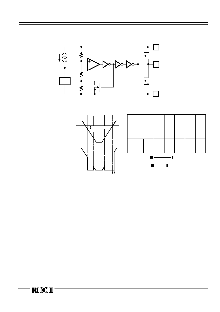
OPERATION
V
DD
OUT
GND
Vref
Ra
Rb
Rc
Pch
Nch
Comparator
Figure 1. Block Diagram
t
PLH
Supply Voltage
(V
DD
)
Output Voltage
(V
OUT
)
Released Voltage(+V
DET
)
Detector Threshold(-V
DET
)
Detector Threshold
Hysteresis
1
2
3
4
5
A
B
Minimum Operating Voltage
GND
GND
Step
1
2
3
4
5
Comparator
Pin Input Voltage
I
II
III
IV
V
Comparator Output
H
L
Inde-
finite
L
H
Tr.1
OFF
ON
Inde-
finite
ON
OFF
Pch
ON
OFF
Inde-
finite
OFF
ON
Output Tr.
Nch
OFF
ON
Inde-
finite
ON
OFF
I.
Rc
Rb
Ra
Rc
Rb
+
+
+
V
DD
II.
Rb
Ra
Rb
+
V
DD
Figure 2. Operation Diagram
Step 1.
Output Voltage is equal to Supply Voltage (V
DD
).
Step 2.
At Point "A", Vref
V
DD
◊
(Rb+Rc)/(Ra+Rb+Rc) is true, as a result, the output of comparator is reverse, and
output voltage becomes to GND level. The voltage level of Point A means detector threshold voltage, or
(-V
DET
).
Step 3.
When the supply voltage is less than minimum operating voltage, the operation of output transistor becomes
indefinite, and in the case that output is pulled up to V
DD
, Output voltage equals to V
DD
voltage.
Step 4.
Output Voltage equals to GND level.
Step 5.
At Point "B", Vref
V
DD
◊
Rb/(Ra+Rb) is true, Output of the comparator is reverse, and output voltage is equal to
the supply voltage, or (V
DD
). The voltage level of Point B means released voltage, or (+V
DET
).
* The difference between Released Voltage and Detector Threshold Voltage is Detector Threshold Hysteresis.
Rev.1.10
- 11 -
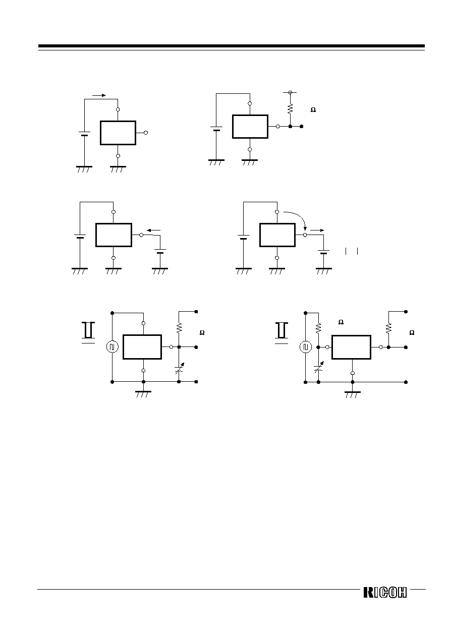
s
TEST CIRCUITS
I
SS
V
DD
OUT
GND
V
IN
R3111
X
Series
R3111
X
Series
V
DD
V
OUT
5.0V
OUT
GND
V
IN
470K
*Pull-up circuit is not necessary for
CMOS Output type, or R3111XXXXC
.
Figure 3. Supply Current Test Circuit
Figure 4. Detector Threshold Test Circuit
V
DD
V
DS
OUT
I
OUT
GND
V
IN
R3111
X
Series
R3111
X
Series
V
DD
V
DD-
V
DS
V
DS
OUT
I
OUT
GND
V
IN
*Apply only to CMOS
Figure 5. Nch Driver Output Current Test Circuit
Figure 6. Pch Driver Output Current Test Circuit
V
DD
V
SS
V
SS
OUT
OUT
GND
P.G.
R3111
XXX
1A
Series
470K
C
OUT
+5.0V
0.7V
R
OUT
+V
DET
+2.0V
OUT
P.G.
V
DD
V
SS
V
SS
OUT
GND
R3111
XXX
1A
Series
470K
100K
C
IN
+5.0V
0.7V
R
OUT
R
IN
+V
DET
+2.0V
Figure 7. Output Delay Time Test Circuit (1)
Figure 8. Output Delay Time Test Circuit (2)
Rev.1.10
- 12 -
s
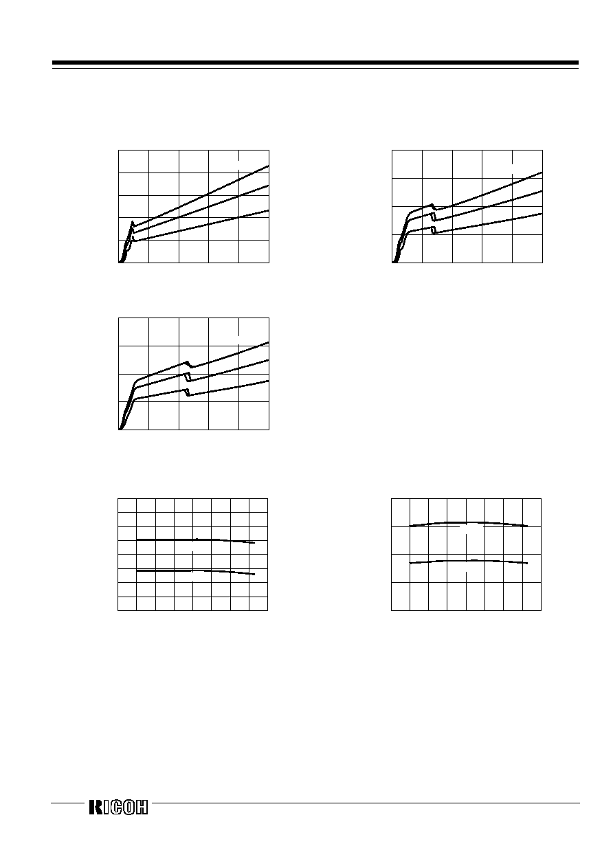
TYPICAL CHARACTERISTICS
1)
Supply Current vs. Input Voltage
R3111x091C
R3111x271C
Topt=85
∞
C
25
∞
C
-40
∞
C
2.5
2.0
1.5
1.0
0.5
0.0
Input Voltage V
IN
(V)
0
2
4
6
8
10
Supply Current I
SS
(
µ
A)
Topt=85
∞
C
25
∞
C
-40
∞
C
2.0
1.5
1.0
0.5
0.0
Input Voltage V
IN
(V)
0
2
4
6
8
10
Supply Current I
SS
(
µ
A)
R3111x451C
Topt=85
∞
C
25
∞
C
-40
∞
C
2.0
1.5
1.0
0.5
0.0
Input Voltage V
IN
(V)
0
2
4
6
8
10
Supply Current I
SS
(
µ
A)
2)
Detector Threshold Hysteresis vs. Temperature
R3111x091C
R3111x271C
+V
DET
-V
DET
1.00
0.98
0.96
0.94
0.92
0.90
0.88
0.84
0.86
Temperature Topt(
∞
C)
-60
0
20
40
60
80
-40
-20
100
Detector Threshold
-V
DET
(V)
2.9
2.8
2.7
2.6
2.5
+V
DET
-V
DET
Temperature Topt(
∞
C)
-60
0
20
40
60
80
-40
-20
100
Detector Threshold
-V
DET
(V)
Rev.1.10
- 13 -
R3111x451C
4.8
4.7
4.6
4.5
4.4
+V
DET
-V
DET
Temperature Topt(
∞
C)
-60
0
20
40
60
80
-40
-20
100
Detector Threshold
-V
DET
(V)
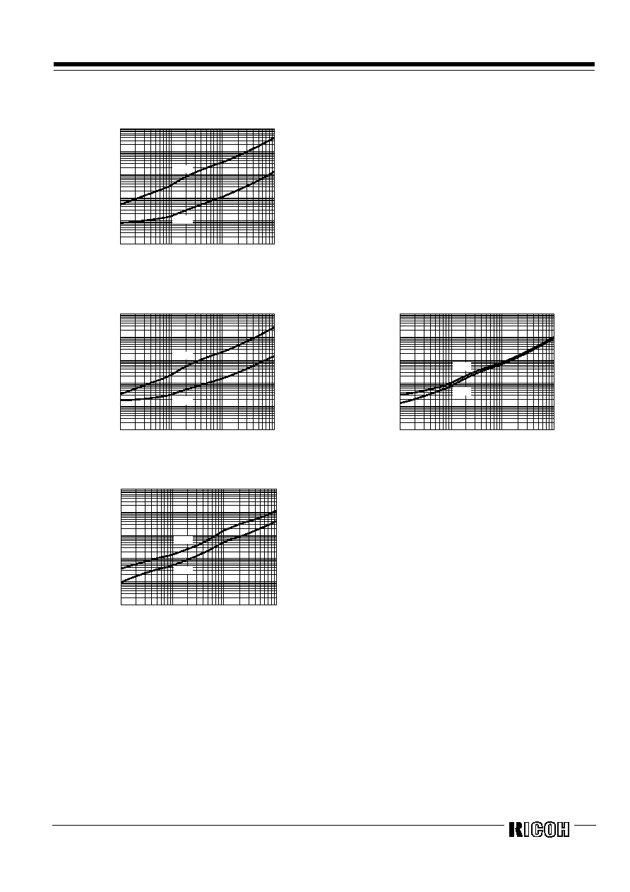
3)
Output Voltage vs. Input Voltage
R3111x091C
R3111x091A
Topt=-40
∞
C
25
∞
C
85
∞
C
V
DD
Pull-up 470k
1.6
1.4
1.2
1.0
0.8
0.6
0.4
0.0
0.2
Input Voltage V
IN
(V)
0
0.6
0.8
1
1.2
1.4
0.2
0.4
1.6
Output V
oltage V
OUT
(V)
5V Pull-up 470k
6
5
4
3
2
0
1
Input Voltage V
IN
(V)
0
0.6
0.8
1
1.2
1.4
0.2
0.4
1.6
Output V
oltage V
OUT
(V)
Topt=-40
∞
C
25
∞
C
85
∞
C
R3111x271C
R3111x271A
Topt=-40
∞
C
25
∞
C
85
∞
C
V
DD
Pull-up 470k
4.0
3.5
3.0
2.5
2.0
1.5
1.0
0.0
0.5
Input Voltage V
IN
(V)
0
1.5
2
2.5
3
3.5
0.5
1
4
Output V
oltage V
OUT
(V)
5V Pull-up 470k
6
5
4
3
2
0
1
Input Voltage V
IN
(V)
0
1.5
2
2.5
3
3.5
0.5
1
4
Output V
oltage V
OUT
(V)
Topt=-40
∞
C
25
∞
C
85
∞
C
Rev.1.10
- 14 -
R3111x451C
R3111x451A
Topt=-40
∞
C
25
∞
C
85
∞
C
V
DD
Pull-up 470k
6
5
4
3
2
0
1
Input Voltage V
IN
(V)
0
2
3
1
6
5
4
Output V
oltage V
OUT
(V)
5V Pull-up 470k
6
5
4
3
2
0
1
Input Voltage V
IN
(V)
0
2
3
1
6
5
4
Output V
oltage V
OUT
(V)
Topt=-40
∞
C
25
∞
C
85
∞
C
4)
Nch Driver Output Current vs. V
DS
R3111x091C
R3111x091C
Topt=25
∞
C
V
DD
=0.85V
0.7V
700
600
500
400
300
200
0
100
V
DS
(V)
0
0.2
0.4
0.6
0.8
Output Current I
OUT
(
µ
A)
V
DD
=0.8V
0.7V
Topt=25
∞
C
300
250
200
150
100
0
50
V
DS
(V)
0
0.02
0.04
0.06
0.08
0.1
Output Current I
OUT
(
µ
A)
R3111x271C
R3111x271C
Topt=25
∞
C
V
DD
=2.5V
2.0V
1.5V
20
18
14
16
12
10
8
6
4
0
2
V
DS
(V)
0
0.5
1
1.5
2
2.5
Output Current I
OUT
(mA)
V
DD
=0.8V
0.7V
Topt=25
∞
C
300
250
200
150
100
0
50
V
DS
(V)
0
0.02
0.04
0.06
0.08
0.1
Output Current I
OUT
(
µ
A)
Rev.1.10
- 15 -
R3111x451C
R3111x451C
Topt=25
∞
C
V
DD
=4.5V
4.0V
3.5V
3.0V
2.5V
2.0V
1.5V
60
50
40
30
20
0
10
V
DS
(V)
0
0.5
1
1.5
2
2.5
3
4
3.5
4.5
Output Current I
OUT
(mA)
V
DD
=0.8V
0.7V
Topt=25
∞
C
300
250
200
150
100
0
50
V
DS
(V)
0
0.02
0.04
0.06
0.08
0.1
Output Current I
OUT
(
µ
A)
5)
Nch Driver Output Current vs. Input Voltage
R3111x091C
R3111x271C
900
800
700
600
500
400
300
200
0
100
Input Voltage V
IN
(V)
0
0.2
0.4
0.6
1
0.8
Output Current I
OUT
(mA)
Topt=-85
∞
C
25
∞
C
-40
∞
C
14
12
10
8
6
4
0
2
Input Voltage V
IN
(V)
0
0.5
1
1.5
1
2.5
3
Output Current I
OUT
(mA)
Topt=-40
∞
C
25
∞
C
85
∞
C
R3111x451C
25
20
15
10
5
0
Input Voltage V
IN
(V)
0
1
2
3
4
5
6
Output Current I
OUT
(mA)
Topt=-40
∞
C
25
∞
C
85
∞
C
Rev.1.10
- 16 -
6)
Pch Driver Output Current vs. Input Voltage
R3111x091C
R3111x271C
Topt=25
∞
C
V
DS
=0.7V
0.5V
1.4
1.2
1.0
0.8
0.6
0.4
0.0
0.2
Input Voltage V
IN
(V)
0
2
4
6
8
Output Current I
OUT
(mA)
Topt=25
∞
C
V
DS
=2.1V
1.5V
0.5V
1.0V
3.5
3.0
2.5
2.0
1.5
1.0
0.0
0.5
Input Voltage V
IN
(V)
0
1
2
4
3
6
5
7
Output Current I
OUT
(mA)
R3111x451C
Topt=25
∞
C
V
DS
=2.1V
1.5V
0.5V
1.0V
4.5
3.5
4.0
3.0
2.5
2.0
1.5
1.0
0.0
0.5
Input Voltage V
IN
(V)
0
2
4
8
6
10
Output Current I
OUT
(mA)
7)
Output Delay Time vs. Load Capacitance
R3111x091A
R3111x271A
tPLH
tPHL
100
10
1
0.1
0.01
0.001
Load Capacitance C
OUT
(
µ
F)
0.0001
0.01
0.001
0.1
Output Dela
y
Time tP(ms)
tPLH
tPHL
100
10
1
0.1
0.01
0.001
Load Capacitance C
OUT
(
µ
F)
0.0001
0.01
0.001
0.1
Output Dela
y
Time tP(ms)
Rev.1.10
- 17 -
R3111x451A
t
PLH
t
PHL
100
10
1
0.1
0.01
0.001
Load Capacitance C
OUT
(
µ
F)
0.0001
0.01
0.001
0.1
Output Dela
y
Time tP(ms)
8)
Output Delay Time vs. Input Pin Capacitance
R3111x091A
R3111x271A
t
PLH
t
PHL
100
10
1
0.1
0.01
0.001
Input Pin Capacitance C
IN
(
µ
F)
0.0001
0.01
0.001
0.1
Output Dela
y
Time tP(ms)
t
PLH
t
PHL
100
10
1
0.1
0.01
0.001
Input Load Capacitance C
IN
(
µ
F)
0.0001
0.01
0.001
0.1
Output Dela
y
Time tP(ms)
R3111x451A
t
PLH
t
PHL
100
10
1
0.1
0.01
0.001
Input Pin Capacitance C
IN
(
µ
F)
0.001
0.1
0.01
1
Output Dela
y
Time tP(ms)
Rev.1.10
- 18 -
s
TYPICAL APPLICATION
q
R3111xxx1A CPU Reset Circuit (Nch Open Drain Output)
Case 1.Input Voltage to R3111xxx1A is equal to
Input Voltage to CPU
Case 2.Input Voltage to R3111xxx1A is unequal to
Input Voltage to CPU
V
DD
V
DD
V
DD
OUT
GND
GND
R3111
XXX
1A
SERIES
470K
CPU
RESET
R
V
DD
V
DD2
V
DD
V
DD1
OUT
GND
GND
R3111
XXX
1A
SERIES
CPU
RESET
R
470K
q
R3111xxx1A CPU Reset Circuit CMOS Output
V
DD
V
DD
V
DD
OUT
GND
GND
R3111
XXX
1C
SERIES
CPU
RESET
q
R3111xxx1A Output Delay Time Circuit 1
(Nch Open Drain Output)
q
R3111xxx1A Output Delay Time Circuit 2
(Nch Open Drain Output)
V
DD
V
DD
V
DD
OUT
GND
GND
R3111
XXX
1A
SERIES
CPU
RESET
R
470K
VDD
V
DD
V
DD
OUT
GND
GND
R3111
XXX
1A
SERIES
CPU
RESET
R2
R1
470K
100K
q
Memory
Back-up
Circuit
V
DD
V
DD
OUT
R3111
XXX
1C
SERIES
D1
V
CC
GND
GND
A
B
G
Y1
Y2
Y3
Y4
D2
V
CC
GND CS
V
CC
GND CS
V
CC
GND CS
V
CC
GND CS
RAM1
RAM2
RAM3
RAM4
Rev.1.10
- 19 -
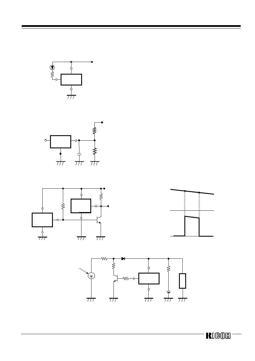
q
Voltage level Indicator Circuit (lighted when the power runs out)
(Nch Open Drain Output)
V
DD
V
DD
OUT
GND
R3111
XXX
1A
SERIES
q
Detector Threshold Adjustable Circuit
(Nch Open Drain Type Output)
V
DD
V
DD
OUT
GND
R3111
XXX
1A
SERIES
C
+
Ra
Rb
Adjusted Detector Threshold
=(-V
DET
)*(Ra+Rb)/Rb
Hysteresis Voltage
=(V
HYS
)*(Ra+Rb)/Rb
*) If the value of Ra is set excessively large, voltage drop may occur
caused by the supply current of IC itself, and detector threshold may
vary.
q
Window Comparator Circuit
(Nch Open Drain Output)
V
DD
V
DD
V
DD
OUT
OUT
OUT
GND
GND
R3111
XXX
1A
SERIES
R3111
XXX
1A
SERIES
V
DET
2
V
DET
1
V
DD
V
SS
V
SS
OUT
V
DET
2
V
DET
1
q
Over-charge Preventing Circuit
V
DD
OUT
GND
R3111
XXX
1C
SERIES
Light
R1
R2
R4
R3
D1
Solar Batter
y
Load

Rev.1.10
- 20 -
TECHNICAL NOTES
V
DD
V
DD
OUT
GND
R3111
SERIES
R
V
DD
V
DD
OUT
GND
R1
R2
R3111
SERIES
Figure 9
Figure 10
1.
In Figure 9, When R3111xxx1C is used, and if an impedance is connected in between Voltage Supplier and the V
DD
Pin of R3111xxx1C Series, the operation might be unstable by through-type current at detection.
When R3111xxx1A is used in Figure 9, if the value of R is set excessively large, voltage drop may occur caused by
supply crrent of IC itself and Detector threshold may vary.
2.
Wiring as shown in Figure 10 may cause the oscillation in both output types of R3111 Series.