
LOW VOLTAGE DETECTOR WITH BUILT-IN
DELAY CIRCUIT
R3132XxxA/C, R3133XxxA/C
1
R3132X_E/2003/10/20
OUTLINE
R3132X/R3133X Series are CMOS-based low voltage detector ICs with built-in delay circuit, high
detector threshold accuracy, and ultra low supply current, which can operate at low voltage.
These ICs can be used as system reset generators, and each of these ICs consists of a voltage ref-
erence, a comparator, resistors for setting voltage detector threshold, an output driver transistor,
manual reset circuit, and an output delay generator.
Detector threshold is fixed internally with high accuracy and requires no adjustment. When a
supply voltage crosses a setting detector threshold voltage from a high value to a lower value, this IC
generates reset signal.
R3132X Series output "L" at its detect, while R3133X Series output "H".
Since each of R3132X/R3133X Series embeds an output delay generator, during a setting 240ms
delay time, which is fixed in the IC, this IC keeps the reset condition after they are released. Released
conditions are the case when a supply voltage crosses a setting detector threshold voltage from a low
value to a higher value, or when this IC is released from manual reset.
Two output types, Nch open drain type and CMOS type, are available.
Since the package for these ICs are ultra small SC-82AB package and SON1612-6(Under Devel-
opment), high density mounting of the ICs on board is possible.
FEATURES
∑
Ultra-low supply current ............................................. Typ. 0.8µA (R313xQ27x: V
DD
=3.0V)
∑
Operating Voltage Range ............................................. 0.8V to 6.0V (Topt=25∞C)
∑
Detector Threshold...................................................... Setting with a step of 0.1V in the range of
1.0V to 5.0V is possible. Further, 2.32V,
2.63V, 2.93V, 3.08V, 4.38V, and 4.63V can
be provided as standard.
∑
Embedded Power on Reset Delay Time Circuit ............. Typ. 240ms
∑
High Accuracy Detector Threshold............................... ±2.0%
∑
High Accuracy Released Delay Time............................. ±15.0%
∑
Low Temperature-Drift Coefficient of Detector Threshold Typ. ±100ppm/∞C
∑
Two Output Types....................................................... Nch Open Drain and CMOS
∑
Small Packages ........................................................... SC-82AB, SON1612-6(Under Development)

R3132XxxA/C, R3133XxxA/C
2
APPLICATIONS
∑
CPU & Logic Circuit Reset
∑
Battery Checker
∑
Window Comparator
∑
Wave Shaping Circuit
∑
Battery Backup Circuit
∑
Power Failure Detector
BLOCK DIAGRAMS
R3132XxxEA Nch Open Drain Output
R3132xxxEC CMOS Output
MR
OUT
V
DD
GND
Vref
+
-
Delay
Circuit
MR
OUT
V
DD
GND
Vref
+
-
Delay
Circuit
R3133xxxEA Nch Open Drain Output
R3133xxxEC CMOS Output
MR
V
OUT
V
DD
GND
Vref
+
-
Delay
Circuit
MR
OUT
V
DD
GND
Vref
+
-
Delay
Circuit
R3132XxxA/C, R3133XxxA/C
3
TIMING CHART
V
SS
V
SS
Tdelay
Tdelay
Detector
Threshold
V
DET
Power
Supply
(V
DD
)
Output Voltage
Manual
Reset
Minimum
Operating
Voltage
V
SS
V
SS
V
SS
V
SS
Tdelay
Tdelay
Detector
Threshold
V
DET
Supply
Voltage
(V
DD
)
Output
Voltage
Manual
Reset
Minimum
Operating
Voltage
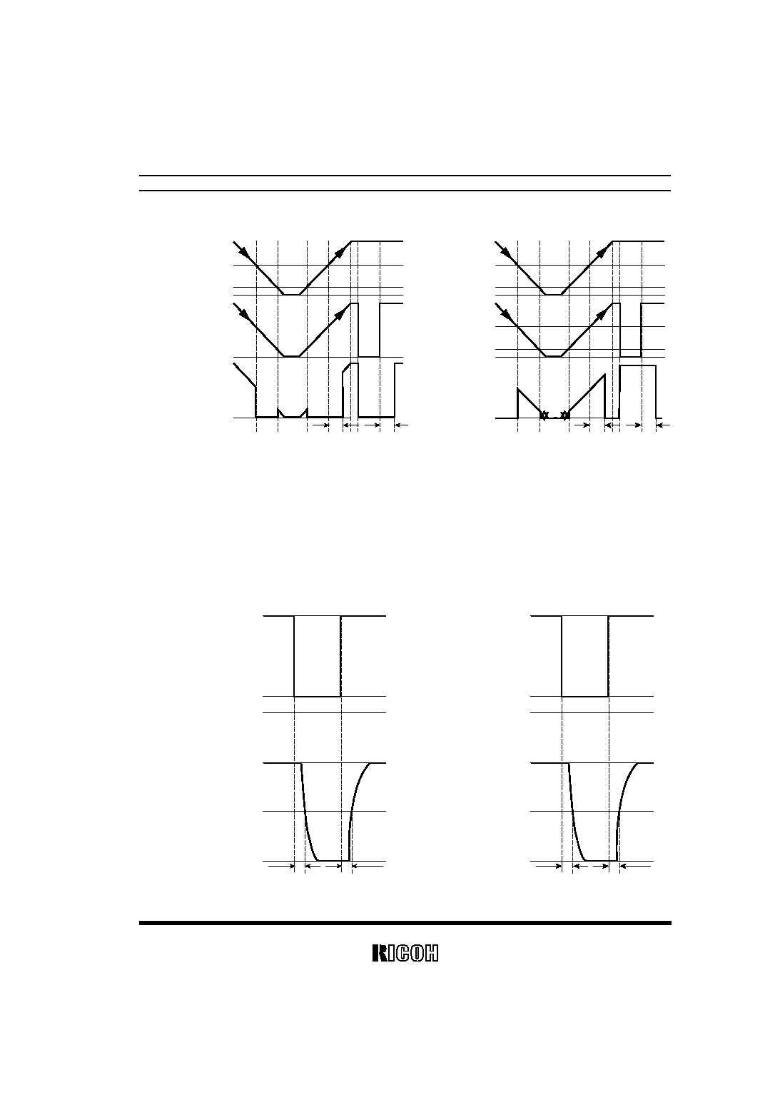
R3132X Operation Diagram
R3133X Operation Diagram
∑
Output Delay Operation
Output Delay Time, or Tdelay is specified as follows:
1. In the case of Nch Open Drain Output:
The time interval from rising edge of V
DD
pulse (0.8V
(V
DET
)+1.0V) to the time at which the output
reaches 2.5V under the condition that the output pin (OUT) is pulled up to 5V through a 470k
resistor.
2. In the case of CMOS Output:
The time interval from rising edge of V
DD
pulse (0.8V
(V
DET
)+1.0V) to the time at the output reaches
V
DD
/2.
0.8V
5.0V
2.5V
GND
GND
+V
DET
+1.0V
Input Voltage
(V
DD
)
Output Voltage
Tdelay
Trst
0.8V
GND
GND
+V
DET
+1.0V
+V
DET
+1.0V
(V
DET
+1.0V)/2
Input Voltage
(V
DD
)
Output Voltage
Tdelay
Trst
Nch Open Drain Output
CMOS Output
R3132XxxA/C, R3133XxxA/C
4
SELECTION GUIDE
The detector threshold and the output type of R3132X/R3133X Series can be designated at the
user's request by specifying the part number as follows:
R3132XxxEx (x)-TR
Part Number
R3133XxxEx (x)-TR
a b b' c d
Code
Contents
a
Package Designation
Q:SC82-AB D: SON1612-6(Under Development)
b/b'
Setting Detector Threshold (V
DET
)
Stepwise setting with a step of 0.1V in the range of 1.0V to 5.0V is possible.
a' describes the last digit of the next items; 2.32V/2.63V/2.93V/3.08V/4.63V
ex. 2.63V Output
R313xX26Ex3-TR
c
Designation of Output type
A: Nch Open Drain
C: CMOS
d
TR: Designation of Taping Direction
(Refer to Taping Specification)
PIN CONFIGURATION
SC
SC
SC
SC----82AB
82AB
82AB
82AB
SON1612-6Under Development
4
3
1
2
(mark side)
6 5 4
1 2 3
R3132XxxA/C, R3133XxxA/C
5
PIN DESCRIPTION
SC82-AB
Pin No.
Symbol
Description
1
GND
Ground Pin
2
OUT
Output Pin
R3132Q Series: Output "L" at detect, Output "H" at release.
R3133Q Series: Output "H" at detect, Output "L" at release.
3
MR
Manual Reset Input Pin
Active at "L" input. Pulled up via 1M
. If MR pin is not necessary,
open this node, or connect to V
DD
.
4
V
DD
Input Pin
SON1612-6(Under Development)
Pin No.
Symbol
Description
1
V
DD
Input Pin
2
GND
Ground Pin
3
MR
Manual Reset Input Pin
Active at "L" input. Pulled up via 1M
. If MR pin is not necessary,
open this node, or connect to V
DD
.
4
OUT
Output Pin
R3132D Series: Output "L" at detect, Output "H" at release.
R3133D Series: Output "H" at detect, Output "L" at release.
5
GND
Ground Pin
6 NC
No
Connection
R3132XxxA/C, R3133XxxA/C
6
ABSOLUTE MAXIMUM RATINGS
Symbol
Item
Rating
Unit
V
DD
Supply Voltage
6.5
V
CMOS
V
SS
-0.3 to V
DD
+0.3
V
V
OUT
Output Voltage
Nch V
SS
-0.3 to 6.5
V
V
MR
Input Voltage
V
SS
-0.3 to V
DD
+0.3
V
I
OUT
Output Current
20
mA
150(SC82-AB)
P
D
Power Dissipation
500(SON1612-6)(Under Develop-
ment)
*Note1
mW
Topt
Operating Temperature
Range
-40 to +85
∞C
Tstg
Storage Temperature
Range
-55 to +125
∞C
Tsolder
Soldering Temperature
260∞C, 10s
*Note 1: This specification is at mounted on board.
P
D
depends on conditions of mounting on board. This specification is based on the meas-
urement at the condition below:
*Measurement Conditions
Environment: Mounted on board (Wind velocity 0m/s)
Board Material: FR-4 (2-layer)
Board dimensions : 40mm x 40mm x t1.6mm
Copper Area : 50%
ABSOLUTE MAXIMUM RATINGS
Absolute Maximum Ratings are threshold limit values that must not be exceeded even for a moment
under any conditions.
Moreover, such values for any items must not be reached simultaneously. Operation above these
absolute maximum ratings may cause degradation or permanent damage to the device. These are
just stress ratings and do not necessarily imply to guarantee operation below these limits.
R3132XxxA/C, R3133XxxA/C
7
ELECTRICAL CHARACTERISTICS
Topt=25∞C
Symbol
Item
Test Conditions
Min.
Typ.
Max.
Unit
Topt=25∞C
0.75
6.00
R3132
-40∞C
Topt
85∞C
0.85
6.00
Topt=25∞C
0.80
6.00
V
DD
Operating Voltage
R3133
-40∞C
Topt
85∞C
0.90
6.00
V
V
DET
Detector Threshold
V
DET
◊
0.98
V
DET
◊
1.02
V
I
SS1
Supply Current1
V
DD
=V
DET
-0.1V, I
OUT
=0A
2.0
µA
I
SS2
Supply Current2
V
DD
=V
DET
+0.1V, I
OUT
=0A
2.0
µA
V
DET
<1.6V
3.6
1.6V
V
DET
<2.7V
3.0
I
SS3
Supply Current3
2.7V
V
DET
V
DD
=6.0V,
I
OUT
=0A
2.5
µA
V
OH
"H" Output Voltage
Refer to the specification table below.
V
V
OL
"L" Output Voltage
Refer to the specification table below.
V
R
MR
MR pin pull-up
resistance
Topt=25∞C
0.5
1.0
4.0
M
Trst
*Note1
Output Delay Time
for detect
V
DD
=V
DET
to V
DET
-0.1V
15
µs
Tdelay
(*2)
Output Delay Time
for release
V
DD
=0.8V to V
DET
+1.0V
204
240
276
ms
V
DET
/
Topt
Detector Threshold
Temperature
Coefficient
-40∞C
Topt
85∞C
±100
ppm
/
∞C
Note1) Guaranteed by design, not mass production tested.

R3132XxxA/C, R3133XxxA/C
8
∑
"H" Output Voltage (V
OH
) table
Topt=25∞C
Products
Test Conditions
Min.
Typ.
Max.
Unit
V
DET
<1.2V
V
DD
=V
DET
+0.1V, I
OH
=-50µA
1.2V
V
DET
<2.0V
V
DD
=V
DET
+0.1V, I
OH
=-150µA
2.0V
V
DET
<3.1V
V
DD
=V
DET
+0.1V, I
OH
=-500µA
R3132Xxx1C
3.1V
V
DET
V
DD
=V
DET
+0.1V, I
OH
=-800µA
0.8
◊
V
DD
V
V
DET
<1.2V
V
DD
=V
DET
-0.1V, I
OH
=-10µA
1.2V
V
DET
<2.0V
V
DD
=V
DET
-0.1V, I
OH
=-100µA
2.0V
V
DET
<3.1V
V
DD
=V
DET
-0.1V, I
OH
=-500µA
R3133Xxx1C
3.1V
V
DET
V
DD
=V
DET
-0.1V, I
OH
=-800µA
0.8
◊
V
DD
V
∑
"L" Output Voltage (V
OL
) table
Topt=25∞C
Symbol
Item
Test Conditions
Min.
Typ.
Max.
Unit
V
DET
<1.2V
V
DD
=V
DET
-0.1V, I
OL
=20µA
1.2V
V
DET
<2.0V
V
DD
=V
DET
+0.1V, I
OL
=750µA
2.0V
V
DET
<3.1V
V
DD
=V
DET
+0.1V, I
OL
=1.2mA
0.3
V
R3132Xxx1x
3.1V
V
DET
V
DD
=V
DET
+0.1V, I
OL
=3.2mA
0.4
V
V
DET
<1.2V
V
DD
=V
DET
-0.1V, I
OH
=20µA
1.2V
V
DET
<2.0V
V
DD
=V
DET
-0.1V, I
OH
=750µA
2.0V
V
DET
<3.1V
V
DD
=V
DET
-0.1V, I
OH
=1.2mA
0.3
V
R3133Xxx1x
3.1V
V
DET
V
DD
=V
DET
-0.1V, I
OH
=3.2mA
0.4
V
R3132XxxA/C, R3133XxxA/C
9
DETECTOR THRESHOLD SPECIFICATIONS BY PART NUMBER
∑
R3132X
Operating Voltage
Detector Threshold
Supply Current 1
V
DD
[V] -V
DET
[V] Is
S1
[
µ
µ
µ
µ
A]
Part Number
Conditions Max.
Conditions Max.
Min. Typ.
Max.
Conditions Typ.
Max.
R3132X23Ex2
2.274 2.320 2.366
R3132X26Ex3
2.578 2.630 2.682
0.8
R3132X29Ex3
2.872 2.930 2.988
R3132X30Ex8
3.019 3.080 3.141
R3132X43Ex8
4.293 4.380 4.467
R3132X46Ex3
Topt=25
∞
C 0.75
-40
∞
C
Topt
85
∞
C
0.85
4.538 4.630 4.722
V
DD
=V
DET
-0.1V
I
OUT
=0A
0.9
2.0
R3132X10Ex
0.980 1.000 1.020
R3132X11Ex
1.078 1.100 1.122
R3132X12Ex
1.176 1.200 1.224
R3132X13Ex
1.274 1.300 1.326
R3132X14Ex
1.372 1.400 1.428
R3132X15Ex
1.470 1.500 1.530
R3132X16Ex
1.568 1.600 1.632
R3132X17Ex
1.666 1.700 1.734
R3132X18Ex
1.764 1.800 1.836
R3132X19Ex
1.862 1.900 1.938
R3132X20Ex
1.960 2.000 2.040
R3132X21Ex
2.058 2.100 2.142
R3132X22Ex
2.156 2.200 2.244
R3132X23Ex
2.254 2.300 2.346
R3132X24Ex
2.352 2.400 2.448
R3132X25Ex
2.450 2.500 2.550
R3132X26Ex
2.548 2.600 2.652
0.8
R3132X27Ex
2.646 2.700 2.754
R3132X28Ex
2.744 2.800 2.856
R3132X29Ex
2.842 2.900 2.958
R3132X30Ex
2.940 3.000 3.060
R3132X31Ex
3.038 3.100 3.162
R3132X32Ex
3.136 3.200 3.264
R3132X33Ex
3.234 3.300 3.366
R3132X34Ex
3.332 3.400 3.468
R3132X35Ex
3.430 3.500 3.570
R3132X36Ex
3.528 3.600 3.672
R3132X37Ex
3.626 3.700 3.774
R3132X38Ex
3.724 3.800 3.876
R3132X39Ex
3.822 3.900 3.978
R3132X40Ex
3.920 4.000 4.080
R3132X41Ex
4.018 4.100 4.182
R3132X42Ex
4.116 4.200 4.284
R3132X43Ex
4.214 4.300 4.386
R3132X44Ex
4.312 4.400 4.488
R3132X45Ex
4.410 4.500 4.590
R3132X46Ex
4.508 4.600 4.692
R3132X47Ex
4.606 4.700 4.794
R3132X48Ex
4.704 4.800 4.896
R3132X49Ex
4.802 4.900 4.998
R3132X50Ex
Topt=25
∞
C 0.75
-40
∞
C
Topt
85
∞
C
0.85
4.900 5.000 5.100
V
DD
=V
DET
-0.1V
I
OUT
=0A
0.9
2.0

R3132XxxA/C, R3133XxxA/C
10
Supply Current 2
Supply Current 3
"H" Output Voltage
I
SS2
[
µ
µ
µ
µ
A] I
SS3
[
µ
µ
µ
µ
A] V
OH
[V]
Conditions Typ.
Max. Conditions Typ.
Max.
Conditions Min.
1.2
3.0
V
DD
=V
DET
+0.1V
I
OH
=-500uA
V
DD
=V
DET
+0.1V
I
OUT
=0A
0.8 2.0
V
DD
=6.0V
I
OUT
=0A
1.0
2.5
V
DD
=V
DET
+0.1V
I
OH
=-800uA
0.8
◊
V
DD
V
DD
=V
DET
+0.1V
I
OH
=-50uA
3.6
V
DD
=V
DET
+0.1V
I
OH
=-150uA
1.4
1.2
3.0
V
DD
=V
DET
+0.1V
I
OH
=-500uA
1.0
V
DD
=V
DET
+0.1V
I
OUT
=0A
0.8 2.0
V
DD
=6.0V
I
OUT
=0A
0.8
2.5
V
DD
=V
DET
+0.1V
I
OH
=-800uA
0.8
◊
V
DD

R3132XxxA/C, R3133XxxA/C
11
"L" Output Voltage
MR pin "H" Input
Voltage
MR pin "L" Input
Voltage
MR pin pull-up resistance
V
OL
[V]
V
IH
[V] V
IL
[V] R
MR
[M
]
Part Number
Conditions Max.
Conditions Min.
Conditions Max. Conditions Min.
Typ.
Max.
R3132X23Ex2
R3132X26Ex3
R3132X29Ex3
R3132X30Ex8
V
DD
=V
DET
-0.1V
I
OL
=+1.2mA
0.3
R3132X43Ex8
R3132X46Ex3
V
DD
=V
DET
-0.1V
I
OL
=+3.2mA
0.4
V
DD
V
DET
+0.1
0.75
◊
V
DD
V
DD
V
DET
+0.1
0.2
◊
V
DD
Topt=25
∞
C 0.5
1.0
4.0
R3132X10Ex
R3132X11Ex
V
DD
=V
DET
-0.1V
I
OL
=+20
µ
A
R3132X12Ex
R3132X13Ex
R3132X14Ex
R3132X15Ex
R3132X16Ex
R3132X17Ex
R3132X18Ex
R3132X19Ex
V
DD
=V
DET
-0.1V
I
OL
=+750
µ
A
R3132X20Ex
R3132X21Ex
R3132X22Ex
R3132X23Ex
R3132X24Ex
R3132X25Ex
R3132X26Ex
R3132X27Ex
R3132X28Ex
R3132X29Ex
R3132X30Ex
V
DD
=V
DET
-0.1V
I
OL
=+1.2mA
0.3
R3132X31Ex
R3132X32Ex
R3132X33Ex
R3132X34Ex
R3132X35Ex
R3132X36Ex
R3132X37Ex
R3132X38Ex
R3132X39Ex
R3132X40Ex
R3132X41Ex
R3132X42Ex
R3132X43Ex
R3132X44Ex
R3132X45Ex
R3132X46Ex
R3132X47Ex
R3132X48Ex
R3132X49Ex
R3132X50Ex
V
DD
=V
DET
-0.1V
I
OL
=+3.2mA
0.4
V
DD
V
DET
+0.1
0.75
◊
V
DD
V
DD
V
DET
+0.1
0.2
◊
V
DD
Topt=25
∞
C 0.5
1.0
4.0
R3132XxxA/C, R3133XxxA/C
12
Output Delay Time for Release
Detector Threshold
Temperature Coefficient
Tdelay[ms]
VDET/
Topt[ppm/
∞
∞
∞
∞
C]
Conditions Min.
Typ.
Max.
Conditions
V
DD
=0.8V
V
DET
+1.0V
Topt=25
∞
C
204 240 276
-40
∞
C
Topt
85
∞
C
±
100
V
DD
=0.8V
V
DET
+1.0V
Topt=25
∞
C
204 240 276
-40
∞
C
Topt
85
∞
C
±
100
R3132XxxA/C, R3133XxxA/C
13
∑
R3133X
Operating Voltage
Detector Threshold
Supply Current 1
V
DD
[V] -V
DET
[V] Iss
1
[
µ
µ
µ
µ
A]
Part Number
Conditions Max.
Conditions Max.
Min. Typ.
Max.
Conditions Typ.
Max.
R3133X23Ex2
2.274 2.320 2.366
R3133X26Ex3
2.578 2.630 2.682
0.8
R3133X29Ex3
2.872 2.930 2.988
R3133X30Ex8
3.019 3.080 3.141
R3133X43Ex8
4.293 4.380 4.467
R3133X46Ex3
Topt=25
∞
C 0.80
-40
∞
C
Topt
85
∞
C
0.90
4.538 4.630 4.722
V
DD
=V
DET
-0.1V
I
OUT
=0A
0.9
2.0
R3133X10Ex
0.980 1.000 1.020
R3133X11Ex
1.078 1.100 1.122
R3133X12Ex
1.176 1.200 1.224
R3133X13Ex
1.274 1.300 1.326
R3133X14Ex
1.372 1.400 1.428
R3133X15Ex
1.470 1.500 1.530
R3133X16Ex
1.568 1.600 1.632
R3133X17Ex
1.666 1.700 1.734
R3133X18Ex
1.764 1.800 1.836
R3133X19Ex
1.862 1.900 1.938
R3133X20Ex
1.960 2.000 2.040
R3133X21Ex
2.058 2.100 2.142
R3133X22Ex
2.156 2.200 2.244
R3133X23Ex
2.254 2.300 2.346
R3133X24Ex
2.352 2.400 2.448
R3133X25Ex
2.450 2.500 2.550
R3133X26Ex
2.548 2.600 2.652
0.8
R3133X27Ex
2.646 2.700 2.754
R3133X28Ex
2.744 2.800 2.856
R3133X29Ex
2.842 2.900 2.958
R3133X30Ex
2.940 3.000 3.060
R3133X31Ex
3.038 3.100 3.162
R3133X32Ex
3.136 3.200 3.264
R3133X33Ex
3.234 3.300 3.366
R3133X34Ex
3.332 3.400 3.468
R3133X35Ex
3.430 3.500 3.570
R3133X36Ex
3.528 3.600 3.672
R3133X37Ex
3.626 3.700 3.774
R3133X38Ex
3.724 3.800 3.876
R3133X39Ex
3.822 3.900 3.978
R3133X40Ex
3.920 4.000 4.080
R3133X41Ex
4.018 4.100 4.182
R3133X42Ex
4.116 4.200 4.284
R3133X43Ex
4.214 4.300 4.386
R3133X44Ex
4.312 4.400 4.488
R3133X45Ex
4.410 4.500 4.590
R3133X46Ex
4.508 4.600 4.692
R3133X47Ex
4.606 4.700 4.794
R3133X48Ex
4.704 4.800 4.896
R3133X49Ex
4.802 4.900 4.998
R3133X50Ex
Topt=25
∞
C 0.80
-40
∞
C
Topt
85
∞
C
0.90
4.900 5.000 5.100
V
DD
=V
DET
-0.1V
I
OUT
=0A
0.9
2.0
R3132XxxA/C, R3133XxxA/C
14
Supply Current 2
Supply Current 3
"H" Output Voltage
I
SS2
[
µ
µ
µ
µ
A] I
SS3
[
µ
µ
µ
µ
A] V
OH
[V]
Conditions Typ.
Max. Conditions Typ.
Max.
Conditions Min.
1.2
3.0
V
DD
=V
DET
-0.1V
I
OH
=-500uA
V
DD
=V
DET
+0.1V
I
OUT
=0A
0.8 2.0
V
DD
=6.0V
I
OUT
=0A
1.0
2.5
V
DD
=V
DET
-0.1V
I
OH
=-800uA
0.8
◊
V
DD
V
DD
=V
DET
-0.1V
I
OH
=-10uA
3.6
V
DD
=V
DET
-0.1V
I
OH
=-100uA
1.4
1.2
3.0
V
DD
=V
DET
-0.1V
I
OH
=-500uA
1.0
V
DD
=V
DET
+0.1V
I
OUT
=0A
0.8 2.0
V
DD
=6.0V
I
OUT
=0A
0.8
2.5
V
DD
=V
DET
-0.1V
I
OH
=-800uA
0.8
◊
V
DD
R3132XxxA/C, R3133XxxA/C
15
"L" Output Voltage
MR pin "H" Input
Voltage
MR pin "L" Input
Voltage
MR pin pull-up resistance
V
OL
[V]
V
IH
[V] V
IL
[V] R
MR
[M
]
Part Number
Conditions Max.
Conditions Max.
Conditions Min.
Conditions Min.
Typ.
Max.
R3133X23Ex2
R3133X26Ex3
R3133X29Ex3
R3133X30Ex8
V
DD
=V
DET
+0.1V
I
OL
=+1.2mA
0.3
R3133X43Ex8
R3133X46Ex3
V
DD
=V
DET
+0.1V
I
OL
=+3.2mA
0.4
V
DD
V
DET
+0.1
0.75
◊
V
DD
V
DD
V
DET
+0.1
0.2
◊
V
DD
Topt=25
∞
C 0.5
1.0
2.0
R3133X10Ex
R3133X11Ex
V
DD
=V
DET
+0.1V
I
OL
=+20
µ
A
R3133X12Ex
R3133X13Ex
R3133X14Ex
R3133X15Ex
R3133X16Ex
R3133X17Ex
R3133X18Ex
R3133X19Ex
V
DD
=V
DET
+0.1V
I
OL
=+750
µ
A
R3133X20Ex
R3133X21Ex
R3133X22Ex
R3133X23Ex
R3133X24Ex
R3133X25Ex
R3133X26Ex
R3133X27Ex
R3133X28Ex
R3133X29Ex
R3133X30Ex
V
DD
=V
DET
+0.1V
I
OL
=+1.2mA
0.3
R3133X31Ex
R3133X32Ex
R3133X33Ex
R3133X34Ex
R3133X35Ex
R3133X36Ex
R3133X37Ex
R3133X38Ex
R3133X39Ex
R3133X40Ex
R3133X41Ex
R3133X42Ex
R3133X43Ex
R3133X44Ex
R3133X45Ex
R3133X46Ex
R3133X47Ex
R3133X48Ex
R3133X49Ex
R3133X50Ex
V
DD
=V
DET
+0.1V
I
OL
=+3.2mA
0.4
V
DD
V
DET
+0.1
0.75
◊
V
DD
V
DD
V
DET
+0.1
0.2
◊
V
DD
Topt=25
∞
C 0.5
1.0
2.0

R3132XxxA/C, R3133XxxA/C
16
Output Delay Time for Release
Detector Threshold
Temperature Coefficient
Tdelay[ms]
VDET/
Topt[ppm/
∞
∞
∞
∞
C]
Conditions Min.
Typ.
Max.
Conditions Typ.
V
DD
=0.8V
V
DET
+1.0V
Topt=25
∞
C
204 240 276
-40
∞
C
Topt
85
∞
C
±
100
V
DD
=0.8V
V
DET
+1.0V
Topt=25
∞
C
204 240 276
-40
∞
C
Topt
85
∞
C
±
100
R3132XxxA/C, R3133XxxA/C
17
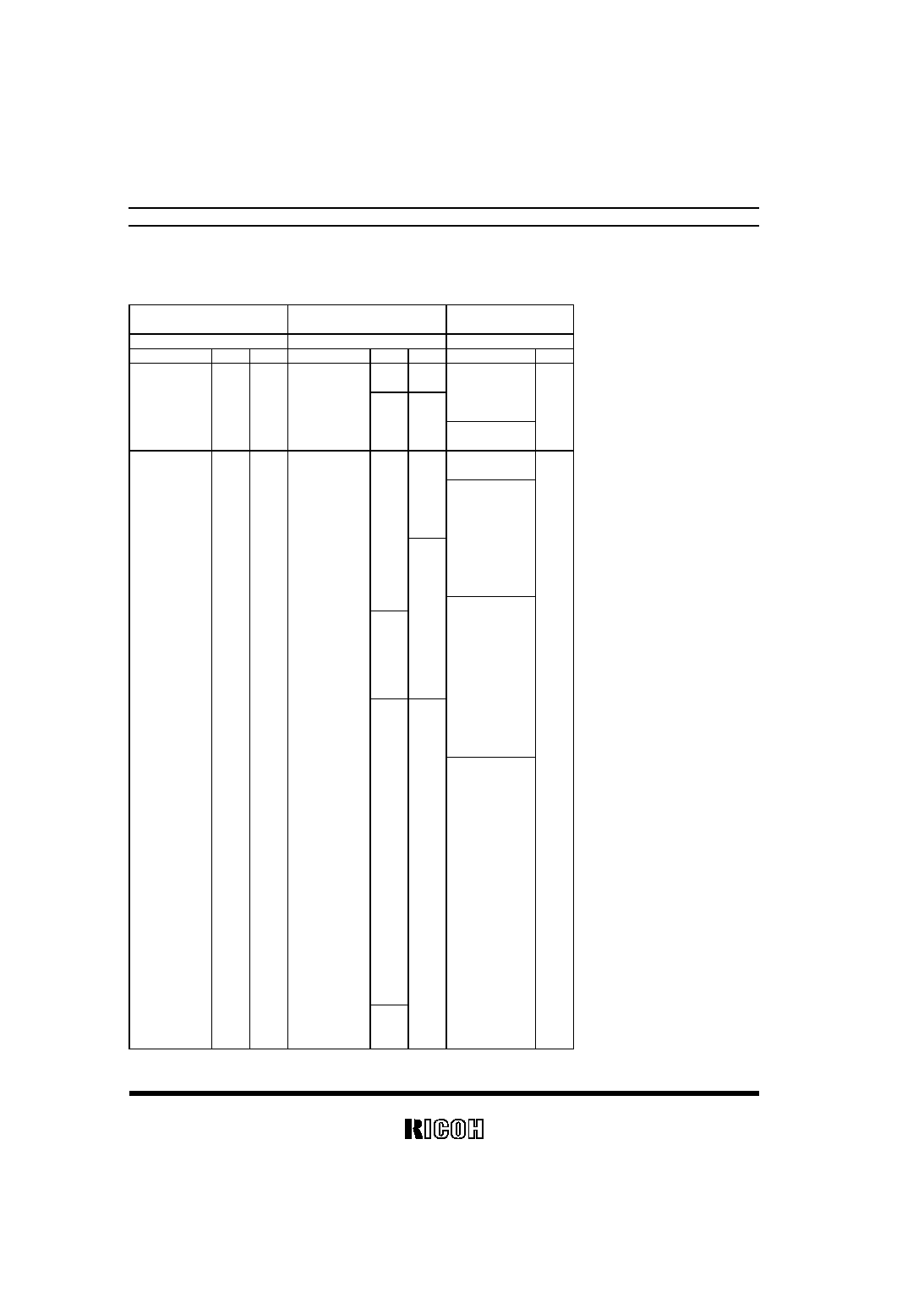
OPERATION
∑
Operation of R3132X Series
OUT
V
DD
GND
Vref
+
-
Nch
Rb
Ra
Pch
Comparator
Delay
Circuit
Block Diagram
∑
CMOS Output Type
OUT pin is connected to the drain of Nch Tr. and Pch Tr. in this IC.
∑
Nch Open Drain Output Type
OUT pin is connected to the drain of Nch Tr. in this IC.
(OUT pin should be pulled up to V
DD
or an external voltage level.)
GND
A
B
1
GND
t
DELAY
Detector Threshold (V
DET
)
=Relased Voltage
Supply
Voltage
(V
DD
)
Output
Voltage
(OUT)
Minimum Operating Voltage
(V
DDL
)
2
3
4
5
Operating Diagram
In the above diagram,
x
Output voltage becomes equal to supply voltage (Nch open drain output type; equal to pull-up
Voltage).
y
When the supply voltage is down to the detector threshold level (Point A), Vref
V
DD
◊
Rb / (Ra+Rb) is
true. Then, the output of the comparator is reversed, thus output voltage becomes equal to GND
level.
z
When the supply voltage is lower than minimum operating voltage, the output of transistor is in-
definite, therefore the output is also indefinite.
{
Output voltage is equal to GND level.
|
When the supply voltage is higher than the released voltage (Point B), Vref
V
DD
◊
Rb / (Ra+Rb) is
true. Then the output of the comparator is reversed, thus the output voltage becomes equal to the
supply voltage (Nch open drain output type; equal to pull-up voltage).
*There is no hysteresis range between the detector threshold and the released voltage.
R3132XxxA/C, R3133XxxA/C
18
∑
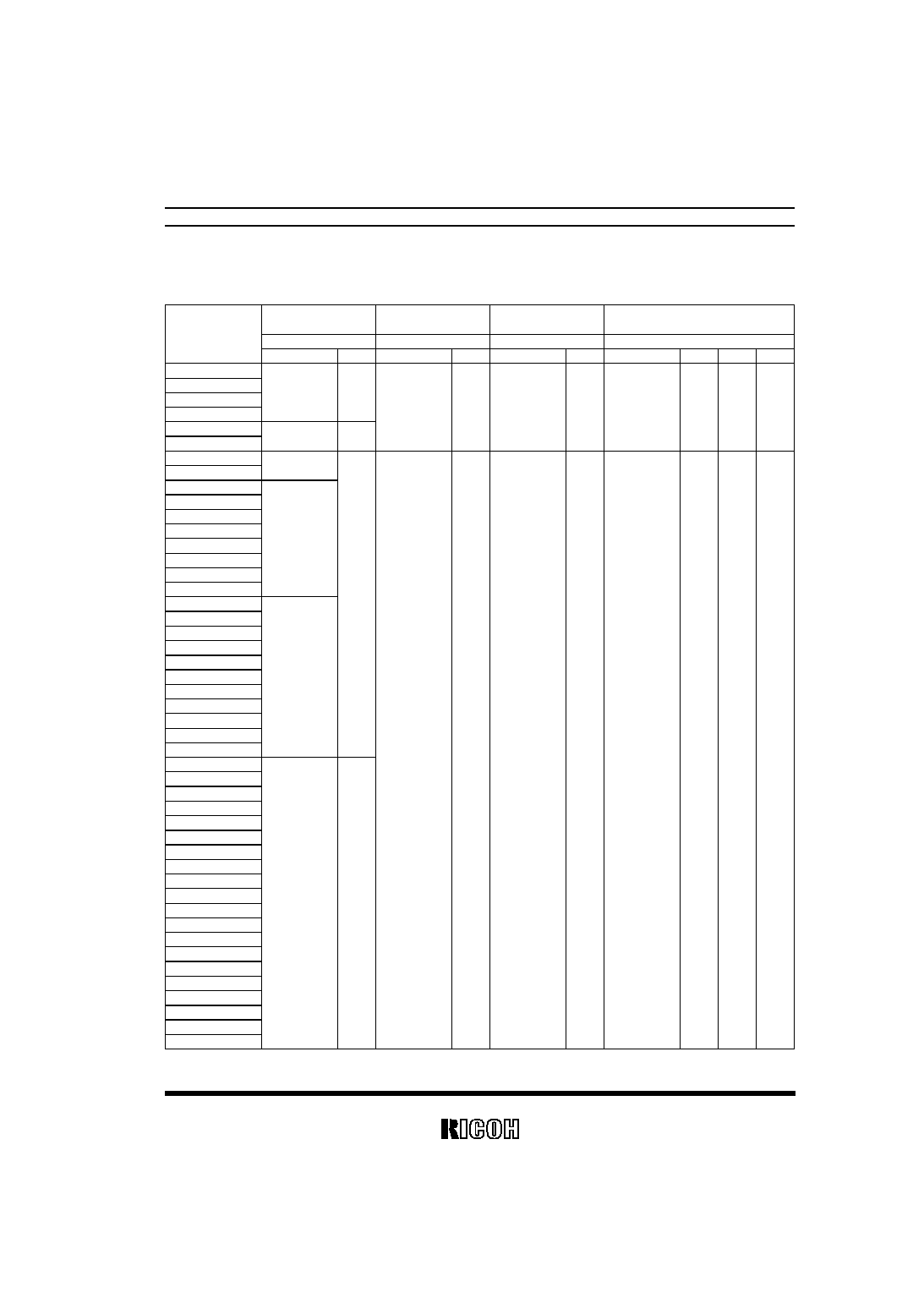
Operation of R3133X Series
OUT
V
DD
GND
Vref
+
-
Nch
Rb
Ra
Pch
Comparator
Delay
Circuit
Block Diagram
∑
CMOS Output Type:
Out pin is connected to the drain of Nch Tr. and Pch Tr. in this IC.
∑
Nch Open Drain Output Type: I
Out pin is connected to the drain of Nch Tr. in this IC.
(OUT pin should be pulled up to V
DD
or an external voltage level.)
GND
A
B
1
GND
t
DELAY
Detector Threshold (V
DET
)
=Released Voltage
Supply
Voltage
(V
DD
)
Output
Voltage
(V
OUT
)
Minimum Operating Voltage
(V
DDL
)
2
3
4
5
Operation Diagram
In the above diagram,
x
Output voltage becomes equal to GND level.
y
When the supply voltage is down to the detector threshold level (Point A), Vref
V
DD
◊
Rb / (Ra+Rb) is
true. Then, the output of the comparator is reversed, thus output voltage becomes equal to the
supply voltage (Nch open drain output type; equal to pull-up voltage).
z
When the supply voltage is lower than minimum operating voltage, the output of transistor is in-
definite, therefore the output is also indefinite. (Nch open drain output type; the output voltage level
is equal to pull-up voltage.)
{
Output voltage is equal to the supply voltage. (Nch open drain output type; equal to pull-up Voltage.)
|
When the supply voltage is higher than the released voltage (Point B), Vref
V
DD
◊
Rb / (Ra+Rb) is
true. Then the output of the comparator is reversed, thus the output voltage becomes equal to GND
level after the output delay time.
*There is no hysteresis range between the detector threshold and the released voltage.
R3132XxxA/C, R3133XxxA/C
19
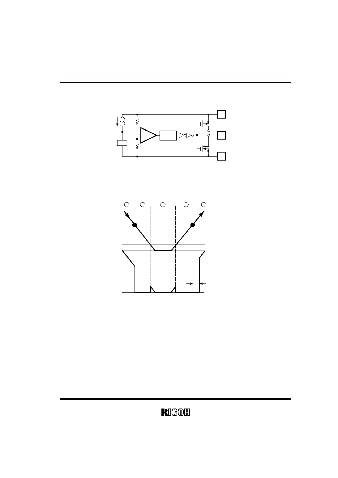
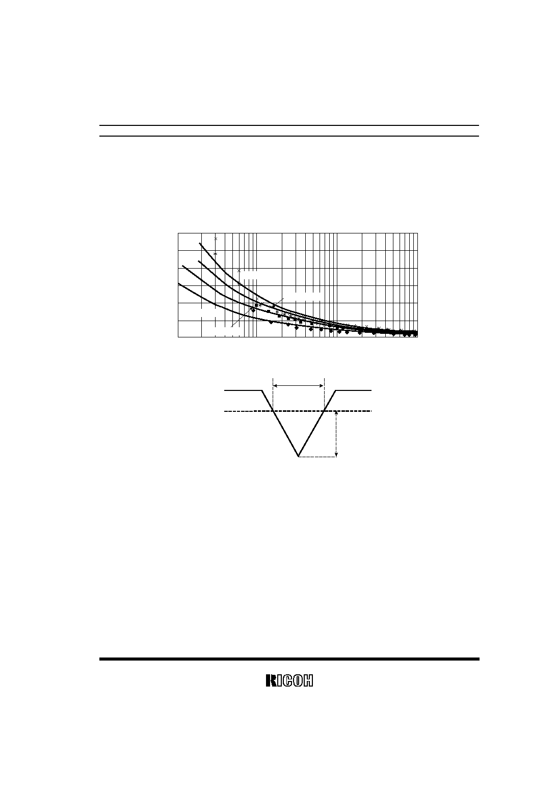
TECHNICAL NOTES
When the IC is released, if a large pulse (glitch) which crosses the detector threshold voltage is in,
the IC may not maintain the released condition. The amplitude of the pulse (V
DET
-V
DD
min) and the pulse
width the IC can maintain the released level is described in the graph as follows:
Reset Comparator Overdrive, (V
DET
-Vddmin) (mV)
0
20
40
60
80
100
120
Pulse width during under V
DET
(
µ
s)
1
10
100
1000
R313xQ36E
R313xQ48E
R313xQ27E
R313xQ10E
V
DET
V
DD
Amplitude level
(V
DET
-V
DDmin
)
Pulse Width
VIN Input Waveform
Notes:
The graph above shows the condition for the maximum transient duration without generating a
reset. If the larger amplitude or larger pulse width noise than the graph may be on the V
DD
, the reset
signal may be generated.

R3132XxxA/C, R3133XxxA/C
20
Application Notes
V
DD
R
V
DD
GND
OUT
R313xQ
Series
V
DD
R1
R2
V
DD
GND
OUT
R313xQ
Series
Figure
A
Figure
B
The connection such as Figure A and Figure B may cause the loop oscillation because of the cross
conduction current. Not only that, these types connection may make shift the detector threshold level
because of the voltage dropout with consumption current of the IC itself.
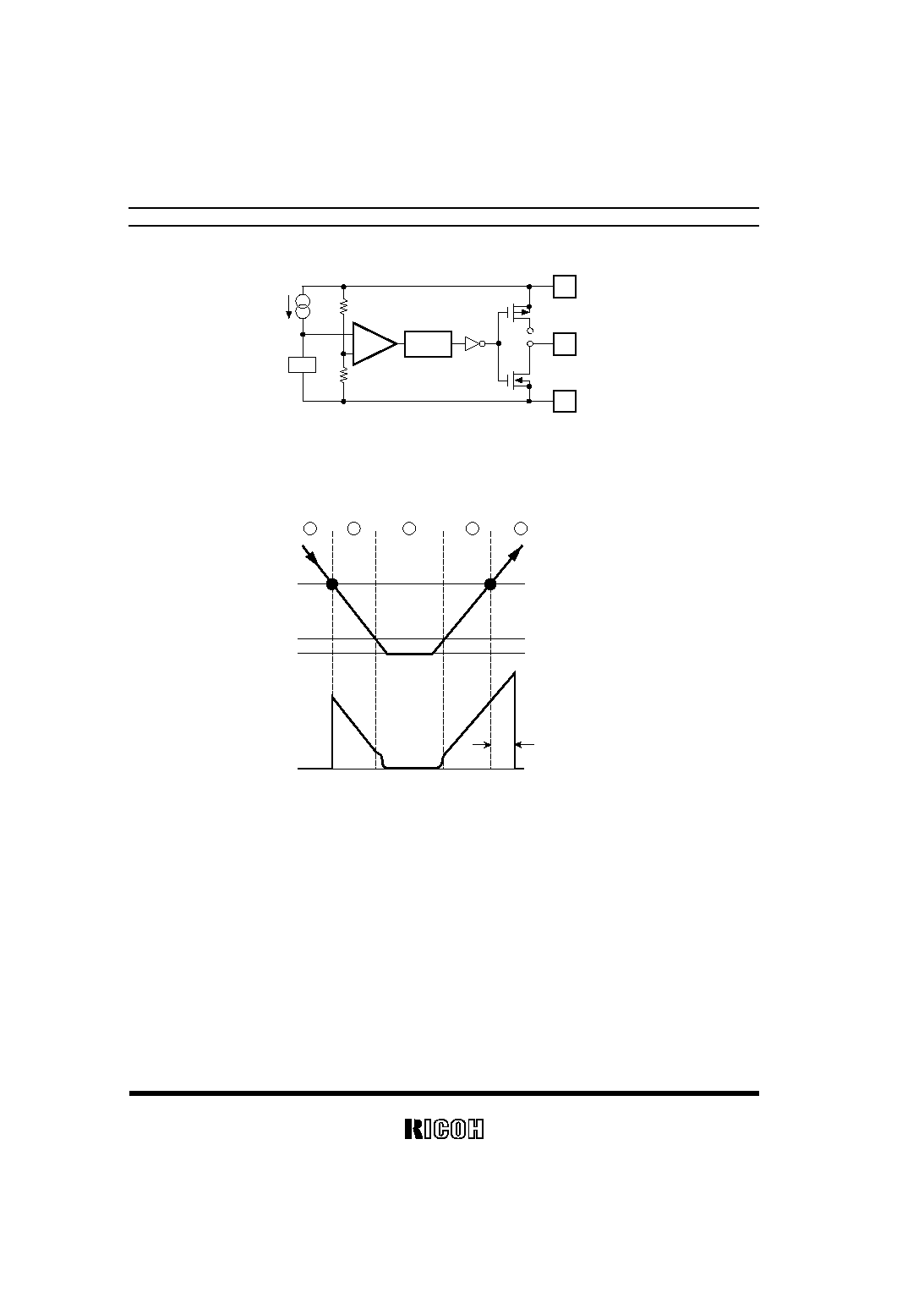
TEST CIRCUITS
∑
Test Circuit for Supply Current
∑
∑
∑
∑
Test Circuit for Detector Threshold
(CMOS Output type; pull-up part is not necessary.)
R313xQ
Series
V
DD
V
IN
I
SS
GND
OUT
R313xQ
Series
V
DD
OUT
MR
5V
470k
V
IN
GND
V
OUT
∑
Test Circuit for "H" Output Voltage
∑
∑
∑
∑
Test Circuit for "L" Output Voltage
(CMOS Output Type only)
R313xQ
Series
V
DD
OUT
V
IN
GND
V
OH
MR
I
OUT
V
R313xQ
Series
V
DD
OUT
V
IN
GND
V
OL
MR
I
OUT
V
R3132XxxA/C, R3133XxxA/C
21
∑
Test Circuit for MR pin Input Voltage
∑
∑
∑
∑
Test Circuit for MR pin Pull-up Resistance
(CMOS Output type; pull-up part is not necessary.)
V
DD
V
IN
GND
5V
470k
MR
V
MR
R313xQ
Series
V
DD
V
IN
GND
V
MR
R313xQ
Series
MR
I
MR
I
SS
∑
Test Circuit for Off Leakage Current
∑
∑
∑
∑
Test Circuit for Output Delay Time
(CMOS Output type; pull-up is not necessary.)
V
DD
OUT
V
IN
V
DS
GND
I
OZ
R313xQ
Series
50%
Tdelay
V
DD
Input
Voltage
Output
Voltage
GND
GND
1.0V
(V
DET
)+1.0V
R3133Q
Series
R3132Q
Series
R313xQ
Series
V
DD
OUT
V
IN
GND
V
OUT
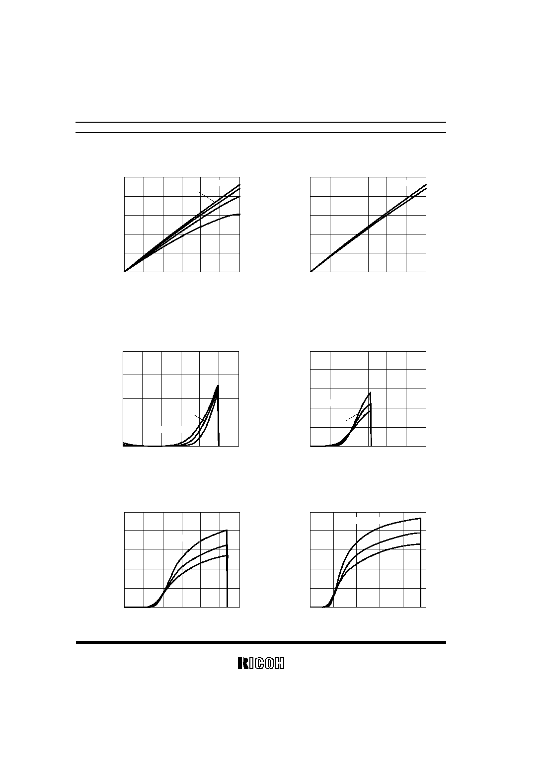
TYPICAL CHARACTERISTICS
1) Supply Current vs. Input Voltage
R3132X101x/R3133X101x
R3132X161x/R3133X161x
2
1.6
1.2
0.8
0
0.4
Input Voltage V
IN
(V)
Supply Current I
SS
(
µ
A)
0
1
2
3
4
6
5
Topt=85
∞
C
25
∞
C
-40
∞
C
2
1.6
1.2
0.8
0
0.4
Input Voltage V
IN
(V)
Supply Current I
SS
(
µ
A)
0
1
2
3
4
6
5
Topt=85
∞
C
25
∞
C
-40
∞
C
R3132XxxA/C, R3133XxxA/C
22
R3132X271x/R3133X271x
R3132X481x/R3133X481x
2
1.6
1.2
0.8
0
0.4
Input Voltage V
IN
(V)
Supply Current I
SS
(
µ
A)
0
1
2
3
4
6
5
Topt=85
∞
C
25
∞
C
-40
∞
C
2
1.6
1.2
0.8
0
0.4
Input Voltage V
IN
(V)
Supply Current I
SS
(
µ
A)
0
1
2
3
4
6
5
Topt=85
∞
C
25
∞
C
-40
∞
C
2) Detector Threshold vs. Temperature
R3132X101x/R3133X101x
R3132X161x/R3133X161x
1.10
1.05
1.00
0.95
0.90
Temperature Topt(
∞
C)
Detector Threshold V
DET
(V)
-50
-25
0
50
25
75
100
1.80
1.70
1.60
1.50
1.40
Temperature Topt(
∞
C)
Detector Threshold V
DET
(V)
-50
-25
0
50
25
75
100
1.45
1.75
1.65
1.55
R3132X271x/R3133X271x
R3132X481x/R3133X481x
2.90
2.80
2.70
2.60
2.50
Temperature Topt(
∞
C)
Detector Threshold V
DET
(V)
-50
-25
0
50
25
75
100
2.55
2.85
2.75
2.65
5.1
4.9
4.8
4.5
Temerature Topt(
∞
C)
Detector Threshold V
DET
(V)
-50
-25
0
50
25
75
100
4.6
5.0
4.7
R3132XxxA/C, R3133XxxA/C
23
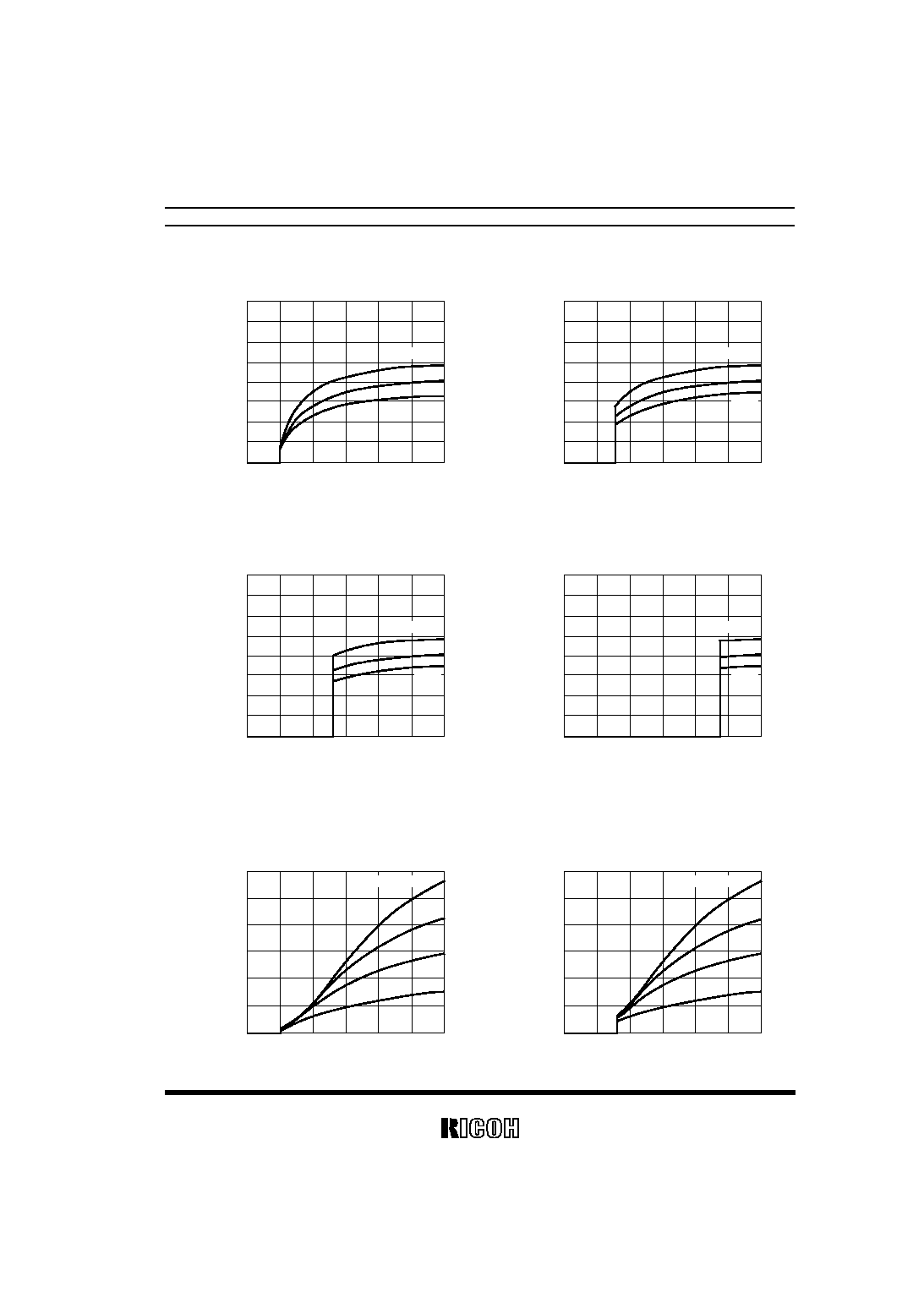
3) Nch Driver Output Current vs. V
DS
(Topt=25
∞
C)
R3132X101x
R3132X161x
1.6
1.4
0.8
0.6
0.2
0
V
DS
(V)
Nch Driver Output Current
I
OUT
(mA)
0
0.2
0.4
0.6
0.8
1.2
1.0
1.2
1.0
0.4
V
DD
=0.99V
0.8V
1.6
1.4
0.8
0.6
0.2
0
V
DS
(V)
Nch Driver Output Current
I
OUT
(mA)
0
0.2
0.4
0.6
0.8
1.2
1.0
1.2
1.0
0.4
V
DD
=1.0V
0.8V
R3132X271x
R3132X481x
15.0
12.5
5.0
2.5
0
V
DS
(V)
Nch Driver Output Current
I
OUT
(mA)
0
0.5
1
2
1.5
10.0
7.5
V
DD
=2.0V
1.0V
30
25
10
5
0
V
DS
(V)
Nch Driver Output Current
I
OUT
(mA)
0
0.5
1
2
1.5
20
15
V
DD
=4.0V
1.0V
2.0V
R3133X101x
R3133X161x
50
40
10
0
V
DS
(V)
Nch Driver Output Current
I
OUT
(mA)
0
1
1.5
3
0.5
2.5
2
30
20
V
DD
=6.0V
2.0V
3.0V
4.0V
5.0V
50
40
10
0
V
DS
(V)
Nch Driver Output Current
I
OUT
(mA)
0
1
1.5
3
0.5
2.5
2
30
20
V
DD
=6.0V
2.0V
3.0V
5.0V
R3132XxxA/C, R3133XxxA/C
24
R3133X271x
R3133X481x
50
40
10
0
V
DS
(V)
Nch Driver Output Current
I
OUT
(mA)
0
1
1.5
3
0.5
2.5
2
30
20
V
DD
=6.0V
3.0V
5.0V
4.0V
50
40
10
0
V
DS
(V)
Nch Driver Output Current
I
OUT
(mA)
0
1
1.5
3
0.5
2.5
2
30
20
VDD=6.0V
5.0V
4) Nch Driver Output Current vs. Input Voltage (V
DS
=0.5V)
R3132X101x
R3132X161x
2.0
1.5
0
Input Voltage V
IN
(V)
Nch Driver Output Current
I
OUT
(mA)
0
0.4
0.6
1.2
0.2
1
0.8
1.0
0.5
Topt=85
∞
C
25
∞
C
-40
∞
C
10
8
0
Input Voltage V
IN
(V)
Nch Driver Output Current
I
OUT
(mA)
0
1
1.5
3
0.5
2.5
2
6
4
2
Topt=-40
∞
C
25
∞
C
85
∞
C
R3132X271x
R3132X481x
10
8
0
Input Voltage V
IN
(V)
Nch Driver Output Current
I
OUT
(mA)
0
1
1.5
3
0.5
2.5
2
6
4
2
Topt=-40
∞
C
25
∞
C
85
∞
C
10
8
0
Input Voltage V
IN
(V)
Nch Driver Output Current
I
OUT
(mA)
0
2
3
5
1
4
6
4
2
Topt=-40
∞
C
25
∞
C
85
∞
C
R3132XxxA/C, R3133XxxA/C
25
R3133X101x
R3133X161x
16
14
0
Input Voltage V
IN
(V)
Nch Driver Output Current
I
OUT
(mA)
0
2
3
6
1
4
5
12
10
8
6
4
2
Topt=-40
∞
C
25
∞
C
85
∞
C
16
14
0
0
2
3
6
1
4
5
12
10
8
6
4
2
Input Voltage V
IN
(V)
Nch Driver Output Current
I
OUT
(mA)
Topt=-40
∞
C
25
∞
C
85
∞
C
R3133X271x
R3133X481x
16
14
0
0
2
3
6
1
4
5
12
10
8
6
4
2
Input Voltage V
IN
(V)
Nch Driver Output Current
I
OUT
(mA)
Topt=-40
∞
C
25
∞
C
85
∞
C
16
14
0
0
2
3
6
1
4
5
12
10
8
6
4
2
Input Voltage V
IN
(V)
Nch Driver Output Current
I
OUT
(mA)
Topt=-40
∞
C
25
∞
C
85
∞
C
5) Pch Driver Output Current vs. Input Voltage
R3132X101x
R3132X161x
12
10
0
0
2
3
6
1
4
5
6
8
4
2
Input Voltage V
IN
(V)
Pch Driver Output Current
I
OUT
(mA)
V
DS
=-2.1V
-1.5V
-1.0V
-0.5V
12
10
0
0
2
3
6
1
4
5
6
8
4
2
Input Voltage V
IN
(V)
Pch Driver Output Current
I
OUT
(mA)
V
DS
=-2.1V
-1.5V
-1.0V
-0.5V
R3132XxxA/C, R3133XxxA/C
26
R3132X271x
R3132X481x
12
10
0
0
2
3
6
1
4
5
6
8
4
2
Input Voltage V
IN
(V)
Pch Driver Output Current
I
OUT
(mA)
V
DS
=-2.1V
-1.5V
-1.0V
-0.5V
12
10
0
0
2
3
6
1
4
5
6
8
4
2
Input Voltage V
IN
(V)
Pch Driver Output Current
I
OUT
(mA)
V
DS
=-2.1V
-1.5V
-1.0V
-0.5V
R3133X101x
R3133X161x
2.0
1.5
0
0
1
2
0.5
1.5
1.0
0.5
Input Voltage V
IN
(V)
Pch Driver Output Current
I
OUT
(mA)
V
DS
=-1.0V,-0.5V
2.0
1.5
0
0
1
2
0.5
1.5
1.0
0.5
Input Voltage V
IN
(V)
Pch Driver Output Current
I
OUT
(mA)
V
DS
=-1.5V,-1.0V
-0.5V
R3133X271x
R3133X481x
5
4
0
0
2
4
1
3
3
2
1
Input Voltage V
IN
(V)
Pch Driver Output Current
I
OUT
(mA)
V
DS
=-2.1V
-1.5V
-1.0V
-0.5V
10
8
0
0
3
6
1
2
4
5
6
4
2
Input Voltage V
IN
(V)
Pch Driver Output Current
I
OUT
(mA)
V
DS
=-2.1V
-1.5V
-1.0V
-0.5V

R3132XxxA/C, R3133XxxA/C
27
6) Output Delay Time at Detection Mode vs. Temperature
R3132X101x/R3133X101x
R3132X161x/R3133X161x
50
40
0
Temperature Topt(
∞
C)
Output Delay Time at Detection Mode
Trst(
µ
s)
-50
25
100
-25
0
50
75
30
20
10
50
40
0
-50
25
100
-25
0
50
75
30
20
10
Temperature Topt(
∞
C)
Output Delay Time at Detection Mode
Trst(
µ
s)
R3132X271x/R3133X271x
R3132X481x/R3133X481x
50
40
0
-50
25
100
-25
0
50
75
30
20
10
Temperature Topt(
∞
C)
Output Delay Time at Detection Mode
Trst(
µ
s)
50
40
0
-50
25
100
-25
0
50
75
30
20
10
Temperature Topt(
∞
C)
Output Delay Time at Detection Mode
Trst(
µ
s)
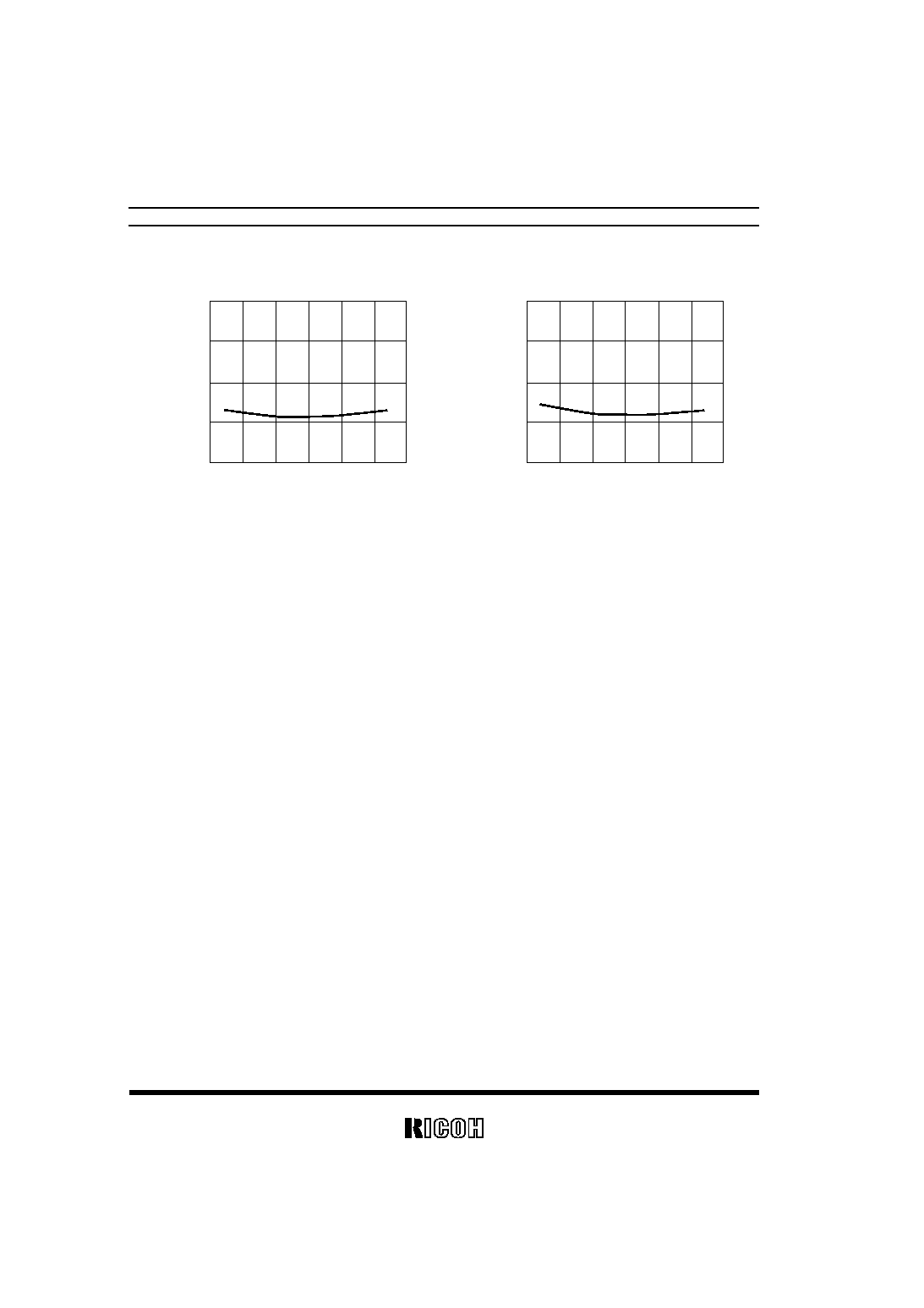
7) Power-on Reset Delay Time vs. Temperature
R3132X101x/R3133X101x
R3132X161x/R3133X161x
360
320
200
Power-on Reset Delay Time
Tdelay(ms)
-50
25
100
-25
0
50
75
280
240
Temperature Topt(
∞
C)
360
320
200
-50
25
100
-25
0
50
75
280
240
Power-on Reset Delay Time
Tdelay(ms)
Temperature Topt(
∞
C)
R3132XxxA/C, R3133XxxA/C
28
R3132X271x/R3133X271x
R3132X481x/R3133X481x
360
320
200
-50
25
100
-25
0
50
75
280
240
Power-on Reset Delay Time
Tdelay(ms)
Temperature Topt(
∞
C)
360
320
200
-50
25
100
-25
0
50
75
280
240
Power-on Reset Delay Time
Tdelay(ms)
Temperature Topt(
∞
C)