
12345
`99.12.3
Microprocessor power management with Watchdog Timer
R5101G Series
12345
Rev. 1.10 - 1 -
n
OUTLINE
The R5101G Series are microprocessor power management ICs with high accuracy output voltage and
detector threshold and with ultra low supply current by CMOS process. Each of these ICs consists of a voltage
regulator, a voltage detector and a watchdog timer. Thus, the R5101G Series have the function of a power
management for microprocessor, a monitor of the voltage of a power source and a microprocessor supervisor.
The built-in voltage regulator with an internal driver transistor can supply typically 50mA current to a system
when the voltage difference between input and output is 2V. Therefore these ICs are very suitable for various
power supply systems for microprocessors. The output voltage is monitored by the voltage detector which is
built-in these ICs.
The built-in voltage detector has an output delay function and the delay time can be set by an external
capacitor(C
D
).
The output voltage and the detector threshold voltage can be set individually for each IC by laser trimming.
Furthermore, when a microprocessor works incorrectly, the watchdog timer which checks over microprocessor
generates reset signals intermittently to prevent a whole system from being malfunction.
The time period for watching and holding a reset signal of the watchdog timer can also be set individually
by an external capacitor(C
TW
).
n
FEATURES
l
Built-in a watchdog timer
l
Time period for monitoring and generating a reset signal of the watchdog timer can be set by an external
capacitor
l
Watchdog timer can be stopped individually by CE Pin
l
Low supply current
∑
∑
∑
∑
∑
∑
∑
∑
∑
∑
∑
∑
∑
∑
∑
∑
∑
∑
∑
∑
∑
∑
∑
TYP. 5µA
l
The output voltage of Voltage Regulator and the detector threshold voltage can be set individually with a step
of 0.1V for each IC by laser trim
l
High Accuracy Output Voltage of Voltage Regulator and Detector Threshold
∑
∑
∑
∑
±2.5%
l
Power-on Reset Delay Time can be set by an external capacitor
l
Output Current
∑
∑
∑
∑
∑
∑
∑
Typ. 50mA (at Vin - Vout = 2V)
l
Small Package
∑
∑
∑
Ultra-mini SSOP-8G (0.65mm pitch ) Refer to Package Dimensions
n
APPLICATION
l
Power source for microprocessors
n
PIN CONFIGURATION
C
TW
C
D
V
DD
V
OUT
SCK
GND
Reset
CE
SSOP8G(0.65mm pitch)

12345
Rev. 1.10 - 2 -
n
PACKAGE DIMENSIONS
n
BLOCK DIAGRAMS
+
-
GND
V
OUT
V
DD
+
-
C
D
W DT
C
TW
SCK
RESET
+
-
Vref1
Vref2
Level Shift
CE
2
6
5
4
1
8
3
7
4.
0
±
0.
3
2.
8
±
0.
2
0.65
2.9
±
0.1
SSOP8G
Unit : mm
12345
Rev. 1.10 - 3 -
n
PIN DESCRIPTION
Pin No. Symbol
Description
1
SCK
Clock Input Pin from Microprocessor
2
CD
External Capacitor Pin for Setting Delay Time of Voltage Detector
3
CTW
External Capacitor Pin for Setting Monitoring Time and Reset Time of Watchdog timer
4
V
DD
Power supply Pin
5
V
OUT
Output Pin for Voltage Regulator
6
GND
Ground Pin
7
CE
Control Switch Pin for Watchdog timer ( "H" active, "L" inactive)
8
RESET Output Pin for Reset signal of Watchdog timer and Voltage Detector.(Output Type is Nch
Open Drain, Output "L" at detecting Detector Threshold and Watchdog Timer Reset. )
n
ABSOLUTE MAXIMUM RATINGS
Topt=25
∞
C, Vss=0V
Symbol
Item
Rating
Unit
V
DD
Supply Voltage
-0.3
~
12
V
V
CD
Voltage of CD Pin
V
ss
-0.3
~
V
DD
+0.3
V
V
CTW
Output Voltage
Voltage of CTW Pin
V
ss
-0.3
~
V
DD
+0.3
V
V
OUT
Voltage of V
OUT
Pin
V
ss
-0.3
~
V
DD
+0.3
V
V
RESET
Voltage of RESET Pin
V
ss
-0.3
~
12
V
V
CE
Input Voltage
Voltage of CE Pin
V
ss
-0.3
~
V
DD
+0.3
V
V
SCK
Voltage of SCK Pin
V
ss
-0.3
~
V
DD
+0.3
V
I
OUT
Current of V
OUT
Pin
150
mA
I
RESET
Output Current
Current of RESET Pin
10
mA
P
D
Power Dissipation
300
mW
T
opt
Operating Temperature Range
-40
~
+85
∞
C
T
stg
Storage Temperature Range
-55
~
+125
∞
C

12345
Rev. 1.10 - 4 -
n
ELECTRICAL CHARACTERISTICS
l
R5101G001A Topt=25
∞
C
Symbol
Item
Conditions
MIN.
TYP.
MAX.
Unit
V
DD
Operating Voltage
10
V
Iss-On
Supply Current (WDT active)
V
DD
=CE=5.0V
5
15
m
A
Iss-Off
Supply Current (WDT inactive)
V
DD
=5.0V, CE=GND
6
18
m
A
V
OUT
Output Voltage
V
DD
=5.0V,I
OUT
=10mA
2.925
3.000
3.075
V
I
OUT
Output Current
V
DD
=5.0V
100
mA
V
DIF
Dropout Voltage
I
OUT
=30mA
150
500
850
mV
D
V
OUT
/
D
I
OUT
Load Regulation
V
DD
=5.0V
1mA
£
I
OUT
£
50mA
50
100
mV
D
V
OUT
/
D
V
DD
Line Regulation
I
OUT
=10mA
V
OUT
+0.5V
£
V
DD
£
10V
0.1
0.2
%/V
Ilim
Current Limit (Short mode)
V
OUT
=0V
10
50
100
mA
D
V
OUT
/
D
Topt
Output Voltage Temperature
Coefficient
I
OUT
=10mA
-40
∞
C
£
Topt
£
85
∞
C
±
100
ppm/
∞
C
-V
DET
Detector Threshold
2.633
2.700
2.767
V
V
HYS
Hysteresis Range
0.081
0.135
0.189
V
V
DETMGN
Regulator Voltage Margin against
Released Voltage
V
OUT
-((-V
DET
)+V
HYS
),
I
OUT
=10mA
0.02
V
D
-V
DET
/
D
Topt
Detector Threshold
Temperature Coefficient
-40
∞
C
£
Topt
£
85
∞
C
±
100
ppm/
∞
C
tpr
Reset Delay Time
V
DD
=5.0V, CD=0.001
m
F
7
14
21
ms
twd
Watch Time of WDT
V
DD
=5.0V, CW=0.01
m
F
50
100
150
ms
twr
Reset Hold Time of WDT
V
DD
=5.0V, CW=0.01
m
F
5
10
15
ms
V
IHSCK
SCK Input Voltage " H "
V
DD
=5.0V
0.8
¥
V
OUT
V
DD
V
V
ILSCK
SCK Input Voltage " L "
V
DD
=5.0V
0
0.2
¥
V
OUT
V
V
IHCE
CE Input Voltage " H "
1.2
V
DD
V
V
ILCE
CE Input Voltage " L "
0
0.2
V
I
IHSCK
SCK Input Current " H "
V
DD
=SCK=5.0V
-1
1
m
A
I
ILSCK
SCK Input Current " L "
V
DD
=5.0V, SCK=GND
-1
1
m
A
Rpu
CE Pull-up Resistance
2
4
10
M
W
I
CD
CD Pin Output Current
V
DD
=1.3V,V
DS
=0.5V
1
2
mA
I
CTW
CTW Pin Output Current
V
DD
=1.3V,V
DS
=0.5V
1
2
mA
I
RESET
RESET Pin Output Current
V
DD
=1.3V,V
DS
=0.5V
1
2
mA
Ileak
RESET Pin Leakage Current
VDD=10.0V,CE=GND,VDS=12.0V
-1
1
m
A
tsckw
SCK Input Pulse Width
V
DD
=5.0V, CW=0.01
m
F
500
ns
Vstart
Minimum Operating Voltage of Voltage Detector
0.9
1.3
V

12345
Rev. 1.10 - 5 -
l
R5101G002A Topt=25
∞
C
Symbol
Item
Conditions
MIN.
TYP.
MAX.
Unit
V
DD
Operating Voltage
10
V
Iss-On
Supply Current (WDT active)
V
DD
=CE5.3V
5
15
m
A
Iss-Off
Supply Current (WDT inactive)
V
DD
=5.3V, CE=GND
6
18
m
A
V
OUT
Output Voltage
V
DD
=5.3V, I
OUT
=10mA
3.218
3.300
3.382
V
I
OUT
Output Current
V
DD
=5.3V
50
mA
V
DIF
Dropout Voltage
I
OUT
=30mA
100
500
650
mV
D
V
OUT
/
D
I
OUT
Load Regulation
V
DD
=5.3V
1mA
£
I
OUT
£
50mA
50
100
mV
D
V
OUT
/
D
V
DD
Line Regulation
I
OUT
=10mA
V
OUT
+0.5V
£
V
DD
£
10V
0.1
0.2
%/V
Ilim
Current Limit (Short mode)
V
OUT
=0V
10
50
100
mA
D
V
OUT
/
D
Topt
Output Voltage Temperature
Coefficient
I
OUT
=10mA
-40
∞
C
£
Topt
£
85
∞
C
±
100
ppm/
∞
C
-V
DET
Detector Threshold
2.925
3.000
3.075
V
V
HYS
Hysteresis Range
0.090
0.150
0.210
V
V
DETMGN
Regulator Voltage Margin
against Released Voltage
V
OUT
-((-V
DET
)+V
HYS
),
I
OUT
=10mA
0.02
V
D
-V
DET
/
D
Topt
Detector Threshold
Temperature Coefficient
-40
∞
C
£
Topt
£
85
∞
C
±
100
ppm/
∞
C
tpr
Reset Delay Time
V
DD
=5.3V, CD=0.001
m
F
7
14
21
ms
twd
Watch Time of WDT
V
DD
=5.3V, CW=0.01
m
F
50
100
150
ms
twr
Reset Hold Time of WDT
V
DD
=5.3V, CW=0.01
m
F
5
10
15
ms
V
IHSCK
SCK Input Voltage " H "
V
DD
=5.3V
0.8
¥
V
OUT
V
DD
V
V
ILSCK
SCK Input Voltage " L "
V
DD
=5.3V
0
0.2
¥
V
OUT
V
V
IHCE
CE Input Voltage " H "
1.2
V
DD
V
V
ILCE
CE Input Voltage " L "
0
0.2
V
I
IHSCK
SCK Input Current " H "
V
DD
=SCK=5.3V
-1
1
m
A
I
ILSCK
SCK Input Current " L "
V
DD
=5.3V, SCK=GND
-1
1
m
A
Rpu
CE Pull-up Resistance
4
M
W
I
CD
CD Pin Output Current
V
DD
=1.3V,V
DS
=0.5V
1
2
mA
I
CTW
CTW Pin Output Current
V
DD
=1.3V,V
DS
=0.5V
1
2
mA
I
RESET
RESET Pin Output Current
V
DD
=1.3V,V
DS
=0.5V
1
2
mA
Ileak
RESET Pin Leakage Current
VDD=10.0V,CE=GND,VDS=12.0V
-1
1
m
A
tsckw
SCK Input Pulse Width
V
DD
=5.3V, SCK=GND
500
ns
Vstart
Minimum Operating Voltage of
Voltage Detector
0.9
1.3
V

12345
Rev. 1.10 - 6 -
l
R5101G003A Topt=25
∞
C
Symbol
Item
Conditions
MIN.
TYP.
MAX.
Unit
V
DD
Operating Voltage
10
V
Iss-On
Supply Current (WDT active)
V
DD
=CE=7.0V
7
20
m
A
Iss-Off
Supply Current (WDT inactive)
V
DD
=7.0V, CE=GND
8
24
m
A
V
OUT
Output Voltage
V
DD
=7.0V, I
OUT
=10mA
4.875
5.000
5.125
V
I
OUT
Output Current
V
DD
=7.0V
50
mA
V
DIF
Dropout Voltage
I
OUT
=30mA
100
350
600
mV
D
V
OUT
/
D
I
OUT
Load Regulation
V
DD
=7.0V
1mA
£
I
OUT
£
50mA
50
100
mV
D
V
OUT
/
D
V
DD
Line Regulation
I
OUT
=10mA
V
OUT
+0.5V
£
VDD
£
10V
0.1
0.2
%/V
Ilim
Current Limit (Short mode)
V
OUT
=0V
10
50
100
mA
D
V
OUT
/
D
Topt
Output Voltage Temperature
Coefficient
I
OUT
=10mA
-40
∞
C
£
Topt
£
85
∞
C
±
100
ppm/
∞
C
-V
DET
Detector Threshold
4.388
4.500
4.590
V
V
HYS
Hysteresis Range
0.135
0.225
0.315
V
V
DETMGN
Regulator Voltage Margin
against Released Voltage
V
OUT
-((-V
DET
)+V
HYS
),
I
OUT
=10mA
0.02
V
D
-V
DET
/
D
Topt
Detector Threshold
Temperature Coefficient
-40
∞
C
£
Topt
£
85
∞
C
±
100
ppm/
∞
C
tpr
Reset Delay Time
V
DD
=7.0V, CD=0.001
m
F
7
14
21
ms
twd
Watch Time of WDT
V
DD
=7.0V, CW=0.01
m
F
50
100
150
ms
twr
Reset Hold Time of WDT
V
DD
=7.0V, CW=0.01
m
F
5
10
15
ms
V
IHSCK
SCK Input Voltage " H "
V
DD
=7.0V
0.8
¥
V
OUT
V
DD
V
V
ILSCK
SCK Input Voltage " L "
V
DD
=7.0V
0
0.2
¥
V
OUT
V
V
IHCE
CE Input Voltage " H "
1.2
V
DD
V
V
ILCE
CE Input Voltage " L "
0
0.2
V
I
IHSCK
SCK Input Current " H "
V
DD
=SCK=7.0V
-1
1
m
A
I
ILSCK
SCK Input Current " L "
V
DD
=7.0V, SCK=GND
-1
1
m
A
Rpu
CE Pull-up Resistance
2
4
10
M
W
I
CD
CD Pin Output Current
V
DD
=1.3V, V
DS
=0.5V
1
2
mA
I
CTW
CTW Pin Output Current
V
DD
=1.3V, V
DS
=0.5V
1
2
mA
I
RESET
RESET Pin Output Current
V
DD
=1.3V, V
DS
=0.5V
1
2
mA
Ileak
RESET Pin Leakage Current
VDD=10.0V, CE=GND,
VDS=12.0V
-1
1
m
A
tsckw
SCK Input Pulse Width
V
DD
=7.0V, SCK=GND
500
ns
Vstart
Minimum Operating Voltage of
Voltage Detector
0.9
1.3
V
12345
Rev. 1.10 - 7 -
l
R5101G004A Topt=25
∞
C
Symbol
Item
Conditions
MIN.
TYP.
MAX.
Unit
V
DD
Operating Voltage
10
V
Iss-On
Supply Current (WDT active)
V
DD
=CE=7.0V
7
20
m
A
Iss-Off
Supply Current (WDT inactive)
V
DD
=7.0V, CE=GND
8
24
m
A
V
OUT
Output Voltage
VDD=7.0V,I
OUT
=10mA
4.875
5.000
5.125
V
I
OUT
Output Current
V
DD
=7.0V
50
mA
V
DIF
Dropout Voltage
I
OUT
=30mA
100
350
650
mV
D
V
OUT
/
D
I
OUT
Load Regulation
V
DD
=7.0V
1mA
£
I
OUT
£
50mA
50
100
mV
D
V
OUT
/
D
V
DD
Line Regulation
I
OUT
=10mA
V
OUT
+0.5V
£
V
DD
£
10V
0.1
0.2
%/V
Ilim
Current Limit (Short mode)
V
OUT
=0V
10
50
100
mA
D
V
OUT
/
D
Topt
Output Voltage Temperature
Coefficient
I
OUT
=10mA
-40
∞
C
£
Topt
£
85
∞
C
±
100
ppm/
∞
C
-V
DET
Detector Threshold
2.145
2.200
2.255
V
V
HYS
Hysteresis Range
0.066
0.110
0.154
V
V
DETMGN
Regulator Voltage Margin
against Released Voltage
V
OUT
-((-V
DET
)+V
HYS
),
I
OUT
=10mA
0.02
V
D
-V
DET
/
D
Topt
Detector Threshold
Temperature Coefficient
-40
∞
C
£
Topt
£
85
∞
C
±
100
ppm/
∞
C
tpr
Reset Delay Time
V
DD
=7.0V, CD=0.001
m
F
7
14
21
ms
twd
Watch Time of WDT
V
DD
=7.0V, CW=0.01
m
F
50
100
150
ms
twr
Reset Hold Time of WDT
V
DD
=7.0V, CW=0.01
m
F
5
10
15
ms
V
IHSCK
SCK Input Voltage " H "
V
DD
=7.0V
0.8
¥
V
OUT
V
DD
V
V
ILSCK
SCK Input Voltage " L "
V
DD
=7.0V
0
0.2
¥
V
OUT
V
V
IHCE
CE Input Voltage " H "
1.2
V
DD
V
V
ILCE
CE Input Voltage " L "
0
0.2
V
I
IHSCK
SCK Input Current " H "
V
DD
=SCK=7.0V
-1
1
m
A
I
ILSCK
SCK Input Current " L "
V
DD
=7.0V, SCK=GND
-1
1
m
A
Rpu
CE Pull-up Resistance
2
4
10
M
W
I
CD
CD Pin Output Current
V
DD
=1.3V, V
DS
=0.5V
1
2
mA
I
CTW
CTW Pin Output Current
V
DD
=1.3V, V
DS
=0.5V
1
2
mA
I
RESET
RESET Pin Output Current
V
DD
=1.3V, V
DS
=0.5V
1
2
mA
Ileak
RESET Pin Leakage Current
VDD=10.0V,CE=GND,VDS=12.0V
-1
1
m
A
tsckw
SCK Input Pulse Width
V
DD
=7.0V, SCK=GND
500
ns
Vstart
Minimum Operating Voltage of
Voltage Detector
0.9
1.3
V

12345
Rev. 1.10 - 8 -
l
R5101G005A Topt=25
∞
C
Symbol
Item
Conditions
MIN.
TYP.
MAX.
Unit
V
DD
Operating Voltage
10
V
Iss-On
Supply Current (WDT active)
V
DD
=CE=4.8V
5
15
m
A
Iss-Off
Supply Current (WDT inactive)
V
DD
=4.8V, CE=GND
6
18
m
A
V
OUT
Output Voltage
V
DD
=4.8V, I
OUT
=10mA
2.730
2.800
2.870
V
I
OUT
Output Current
V
DD
=4.8V, I
OUT
=10mA
50
mA
V
DIF
Dropout Voltage
I
OUT
=10mA
100
350
650
mV
D
V
OUT
/
D
I
OUT
Load Regulation
V
DD
=4.8V
1mA
£
I
OUT
£
50mA
50
100
mV
D
V
OUT
/
D
V
DD
Line Regulation
I
OUT
=10mA
V
OUT
+0.5V
£
V
DD
£
10V
0.1
0.2
%/V
Ilim
Current Limit (Short mode)
V
OUT
=0V
10
50
100
mA
D
V
OUT
/
D
Topt
Output Voltage Temperature
Coefficient
I
OUT
=10mA
-40
∞
C
£
Topt
£
85
∞
C
±
100
ppm/
∞
C
-V
DET
Detector Threshold
2.340
2.400
2.460
V
V
HYS
Hysteresis Range
0.072
0.120
0.168
V
V
DETMGN
Regulator Voltage Margin
against Released Voltage
V
OUT
-((-V
DET
)+V
HYS
),
I
OUT
=10mA
0.02
V
D
-V
DET
/
D
Topt
Detector Threshold
Temperature Coefficient
-40
∞
C
£
Topt
£
85
∞
C
±
100
ppm/
∞
C
tpr
Reset Delay Time
V
DD
=4.8V, CD=0.001
m
F
7
14
21
ms
twd
Watch Time of WDT
V
DD
=4.8V, CW=0.01
m
F
50
100
150
ms
twr
Reset Hold Time of WDT
V
DD
=4.8V, CW=0.01
m
F
5
10
15
ms
V
IHSCK
SCK Input Voltage " H "
V
DD
=4.8V
0.8
¥
V
OUT
V
DD
V
V
ILSCK
SCK Input Voltage " L "
V
DD
=4.8V
0
0.1
¥
V
OUT
V
V
IHCE
CE Input Voltage " H "
1.2
V
DD
V
V
ILCE
CE Input Voltage " L "
0
0.2
V
I
IHSCK
SCK Input Current " H "
V
DD
=SCK=4.8V
-1
1
m
A
I
ILSCK
SCK Input Current
"
L
"
V
DD
=4.8V, SCK=GND
-1
1
m
A
Rpu
CE Pull-up Resistance
4
M
W
I
CD
CD Pin Output Current
V
DD
=1.3V, V
DS
=0.5V
1
2
mA
I
CTW
CTW Pin Output Current
V
DD
=1.3V, V
DS
=0.5V
1
2
mA
I
RESET
RESET Pin Output Current
V
DD
=1.3V, V
DS
=0.5V
1
2
mA
Ileak
RESET Pin Leakage Current
VDD=10.0V,CE=GND,VDS=12.0V
-1
1
m
A
tsckw
SCK Input Pulse Width
V
DD
=4.8V, SCK=GND
500
ns
Vstart
Minimum Operating Voltage of
Voltage Detector
0.9
1.3
V

12345
Rev. 1.10 - 9 -
n
n
n
n
TYPICAL APPLICATION
n
TECHNICAL NOTES
Use 0.01
m
F or more value of an external capacitor, CW for setting monitoring time of watchdog timer.
Use 1 or 2.2
m
F capacitor between V
DD
and GND, and between V
OUT
and GND and make its wiring as short as
possible.
C
TW
C
D
V
DD
V
OUT
SCK
GND
RESET
CE
D
OUT
RESET
V
DD
Micro Processor
R5101GXXX Series
C
D(0.001
m
F)
C
W
(0.01
m
F)
510k
W
1
m
F
1
m
F
12345
Rev. 1.10 - 10 -
n
OPERATION DIAGRAM
V
DD
V
OUT
CD
CTW
SCK
CE
RESET
+Vdet
-Vdet
Detector Threshold Hysteresis
Vref2H
Vref2H
Vref2L
tpr
twd
twr
tsckw
Vstart
¨ - Æ Ø ∞
∞
± ≤
±
∞ ≥ - Æ
∞ ¥
≥
¥
≤

12345
Rev. 1.10 - 11 -
n
OPERATION
¨
When V
DD
is turned on and Input Voltage reaches Vstart (nearly equal 0.8V), the output of RESET pin
becomes "L" level.
-
An External Capacitor starts to be charged through the C
D
pin when an Output Voltage of the Voltage
Regulator, V
OUT
, crosses the Released Voltage , +V
DET
, from Lower to Higher . The V
RESET
is kept "L" level
until Voltage of the C
D
pin , V
CD
, reaches to the Vref2H , about 1.0V , and after that the V
RESET
becomes to
"H" level.
\
tPR : Time interval between the timing of starting edge of forcing voltage to VDD pin and the timing of
reverse the voltage level of V
RESET
.
tPR can be set by connecting an external capacitor to C
D
pin, tPR can be calculated as shown below;
tPR (ms)
ª
13000
¥
C
D
(
m
F) ; C
D means a value of an external capacitor connected to C
D
pin.
Æ
When the voltage level of V
CD
reaches to the Vref2H, the external capacitor starts to be charged through
the C
TW
pin and the watchdog timer begins to operate.
Ø
The operation mode for
t
he external capacitor changes from charging mode to discharging mode through
C
TW
pin when the voltage level of C
TW
pin , V
CTW
, reaches to the Vref2H.
∞
While the C
TW
pin is on the discharging mode, if a clock pulse is entered (synchronous with a rising edge
of the pulse), the operation mode of C
TW
pin changes from charging mode to discharging mode. And
the external capacitor connected to C
TW
pin is charged until its voltage level reaches to Vref2H.
±
While the C
TW
pin
is on the discharging mode, if VCTW level drops to Vref2L, about 0.2V without clock
pulse to CLK pin, the voltage level of Reset pin becomes from "H" to "L".
\
Watch Time of the watchdog timer , tWD , : Discharging Time of C
TW
pin level from Vref2H to Vref2L
tWD can be set by connecting an external capacitor to C
W
pin, tWD can be calculated as shown below;
tWD (ms)
ª
10000
¥
C
W
(
m
F);
Cw means a value of an external capacitor connected to Cw pin.
≤
C
TW
pin is changed to charging mode from discharging mode when the Reset signal is generated.
\
Reset time of the watchdog timer , tWR , : Time interval between Charging time of the C
TW
pin from Vref2L
to Vref2H. tWR can be calculated by the next equation as shown below;
tWR (ms)
ª
tWD/10
≥
The Output Voltage level of Reset pin becomes from "H" to "L", or a Reset signal is generated when an
output voltage of the Voltage Regulator drops to a level at equal or less than -Vdet.
¥
The watchdog timer will be halted when a Voltage level of CE pin becomes to "L". In this case, only the
watchdog timer is stopped and monitoring the output voltage is continued. After that, if the voltage level of CE
pin becomes to "H", C
TW
pin starts to be on charging mode.
12345
Rev. 1.10 - 12 -
n
n
n
n
TEST CIRCUITS
A
GND
V
DD
CE
V
OUT
RESET
SCK
CD
CTW
Test Circuit of Supply Current
Test Circuit of Output Voltage
V
GND
V
DD
CE
V
OUT
RESET
SCK
CD
CTW
I
OUT
Test Circuit of Detector Threshold(V
DET
)
GND
V
DD
CE
V
OUT
RESET
SCK
CD
CTW
470k
Test Circuit of Monitoring Time of WDT and
RESET Time
GND
V
DD
CE
V
OUT
RESET
SCK
CD
CTW
470k
oscilloscope

12345
Rev. 1.10 - 13 -
Test Circuit of RESET Output leakage Current
Test Circuit of SCK Input Current
Test Circuit of Minimum Input Voltage
for RESET Output
Test Circuit of Output Current
GND
V
DD
CE
V
OUT
RESET
SCK
CD
CTW
A
GND
V
DD
CE
V
OUT
RESET
SCK
CD
CTW
A
GND
V
DD
CE
V
OUT
RESET
SCK
CD
CTW
A
GND
V
DD
CE
V
OUT
RESET
SCK
CD
CTW
470K
V
12345
Rev. 1.10 - 14 -
n
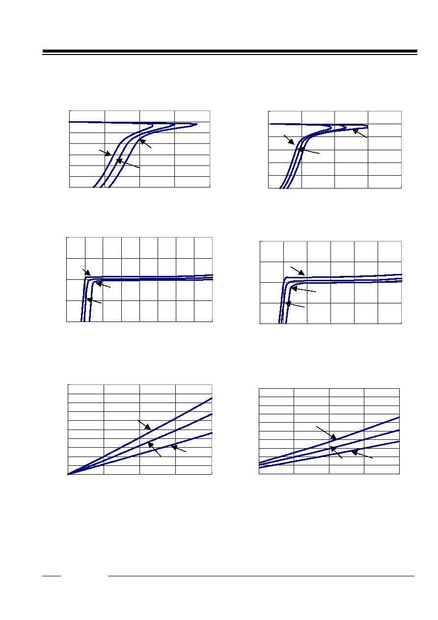
TYPICAL CHARACTERISTICS
1) Output Voltage vs. Output Current
R5101G001A V
DD
=5V
0.0
0.5
1.0
1.5
2.0
2.5
3.0
3.5
0
50
100
150
200
Output Current I
OUT
(mA)
Output Voltage V
OUT
(V)
-40
25
85
R5101G003A,004A V
DD
=7V
0.0
1.0
2.0
3.0
4.0
5.0
6.0
0
100
200
300
400
Output Current I
OUT
(mA)
Output Voltage
V
OUT
(V)
-40
0
85
2) Output Voltage vs. Input Voltage
2.8
2.9
3.0
3.1
3.2
2
3
4
5
6
7
8
9
10
Input Voltage V
DD
(V)
Output Voltage V
OUT
(V)
R5101G001A Topt=25
0mA
10mA
30mA
R5101G003A,004A Topt=25
4.8
4.9
5.0
5.1
5.2
4
5
6
7
8
9
10
Input Voltage V
DD
(V)
Output Voltage V
OUT
(V)
10mA
30mA
0mA
3) Dropout Voltage vs. Output Current
R5101G001A
0.0
0.2
0.4
0.6
0.8
1.0
0
10
20
30
40
Output Current I
OUT
(mA)
Dropout Voltage V
DIF
(V)
-40
25
85
R5101G003A, 004A V
DD
=7.0V
0.0
0.2
0.4
0.6
0.8
1.0
10
20
30
40
50
Output Current I
OUT
(mA)
Dropout Voltage V
DIF
(V)
85
25
-40
∞
C
∞
C
∞
C
∞
C
∞
C
∞
C
∞
C
∞
C
∞
C
∞
C
∞
C
∞
C
∞
C
∞
C

12345
Rev. 1.10 - 15 -
4) Output Voltage vs. Temperature
R5101G001A V
DD
=5V
2.90
2.95
3.00
3.05
3.10
-50
-25
0
25
50
75
100
Temperature Topt
Output Voltage V
OUT
(V)
R5101G003A,004A V
DD
=7.0V,I
OUT
=10mA
4.90
4.95
5.00
5.05
5.10
-50
-25
0
25
50
75
100
Temperature Topt
Output Voltage V
OUT
(V)
5) RESET Pin Voltage vs. Input Voltage 6) Detector Threshold vs. Temperature
R5101G001A Pull-up 510k
0.0
0.5
1.0
1.5
2.0
2.5
3.0
0.0
0.5
1.0
1.5
2.0
2.5
3.0
Input Voltage V
DD
(V)
RESET Pin Voltage V
RESET
(V)
-40
25
85
R5101G001A
2.60
2.65
2.70
2.75
2.80
2.85
2.90
-50
-25
0
25
50
75
100
Temperature Topt
Detector Threshold V
DET
(V)
+V
DET
-V
DET
7) CD Pin Output Current vs. Input Voltage 8) CTW Pin Output Current vs. Input Voltage
R5101G001A V
DS
=0.5V
0
2
4
6
8
10
12
0
1
2
3
Input Voltage V
DD
(V)
CD Output Current I
OUT
(mA)
85
25
-40
R5101G001A V
DS
=0.5V
0
2
4
6
8
10
12
0
1
2
3
Input Voltage V
DD
(V)
CTW Output Current I
OUT
(mA)
-40
25
85
(
∞
C)
(
∞
C)
∞
C
∞
C
∞
C
W
(
∞
C)
∞
C
∞
C
∞
C
∞
C
∞
C
∞
C

12345
Rev. 1.10 - 16 -
9) RESET Pin Output Current vs. Input Voltage 10) Delay Time of Released Voltage vs. Temperature
R5101G001A V
DS
=0.5V
0
2
4
6
8
10
12
0
0.5
1
1.5
2
2.5
3
Input Voltage V
DD
(V)
RESET Output Current I
OUT
(mA)
-40
25
85
R5101G001A
0
2
4
6
8
10
12
14
16
18
20
22
-50
-25
0
25
50
75
100
Temperature Topt
Delay Time of Released Voltage tpr(ms)
11)
Monitoring Time of Watchdog Timer vs. Temperature
12) Reset Time of Watchdog Timer vs. Temperature
R5101G001A
0
20
40
60
80
100
120
140
160
-50
-25
0
25
50
75
100
Temperature Topt
Monitoring Time of Watchdog
Timer twd(ms)
R5101G001A
0
2
4
6
8
10
12
14
16
-50
-25
0
25
50
75
100
Temperature Topt
Reset Time of Watchdog Timer
twr(ms)
13) tpr vs. External Capacitance of Cd Pin 14) twd, twr vs. External Capacitance of Ctw Pin
1
10
100
1000
10000
100000
1.E-09
1.E-08
1.E-07
1.E-06
External Capacitance of CD Pin(F)
tpr (ms)
0.1
1
10
100
1000
10000
100000
1.E-08
1.E-07
1.E-06
External Capacitance of CTW Pin(F)
twd,twr (ms)
twd
twr
∞
C
∞
C
∞
C
(
∞
C)
(
∞
C)
(
∞
C)

12345
Rev. 1.10 - 17 -
15) CE Pull-up Resistance vs. Temperature
R5101G001A
0
1
2
3
4
5
6
7
8
9
10
-50
-25
0
25
50
75
100
Temperature Topt
CE Pull-up Resistance R
PU
16) Supply Current vs. Input Voltage (WDT ON) 17) Supply Current vs. Temperature (WDT ON)
R5101G001A Topt=25
0
3
6
9
12
15
3
4
5
6
7
8
9
10
Input Voltage V
DD
(V)
Supply Current Iss-on(uA)
R5101G001A V
DD
=5V
0
3
6
9
12
15
-50
-25
0
25
50
75
100
Temperature Topt
Supply Current Iss-off
(uA)
18) Supply Current vs. Input Voltage (WDT OFF) 19) Supply Current vs. Temperature (WDT OFF)
R5101G001A Topt=25
0
3
6
9
12
15
18
3
4
5
6
7
8
9
10
Input Voltage V
DD
(V)
Supply Current Iss-off(uA)
R5101G001A V
DD
=5V
0
3
6
9
12
15
18
-50
-25
0
25
50
75
100
Temperature Topt
Supply Current Iss-
on(uA)
(M
W
)
(
∞
C)
∞
C
(
∞
C)
∞
C
(
∞
C)