
'99.9.21
Li-Ion BATTERY PROTECTOR
R5421NxxxC/xxxF series
Rev.1.11
- 1 -
s
OUTLINE
The R5421NxxxC/F Series are protection ICs for over-charge/discharge of rechargeable one-cell Lithium-ion (Li+) excess load
current, further include a short circuit protector for preventing large external short circuit current.
Each of these ICs is composed of three voltage detectors, a reference unit, a delay circuit, a short circuit protector, and a logic
circuit. When charging voltage crosses the detector threshold from a low value to a value higher than V
DET1
, the output of C
OUT
pin, the output of over-charge detector/VD1, switches to low level, charger's negative pin level. After detecting over-charge the
VD1 can be reset and the output of C
OUT
becomes high when the V
DD
voltage is coming down to a level lower than "V
REL1
", or
when a kind of loading is connected to V
DD
after a charger is disconnected from the battery pack while the V
DD
level is in
between "V
DET1
" and "V
REL1
" in the R5421NxxxC/F version.
The output of D
OUT
pin, the output of over-discharge detector/VD2, switches to low level after internally fixed delay time
passed, when discharging voltage crosses the detector threshold from a high value to a value lower than V
DET2
.
After R5421NxxxC/F Series detect the over-discharge voltage, connect a charger to the battery pack, and when the battery
supply voltage becomes higher than the over-discharge detector threshold, VD2 is released and the voltage of D
OUT
becomes
"H" level. In the case of F version, after detecting the over-discharge detection, when the battery supply voltage becomes
equal or higher than over-discharge released voltage, VD2 is also released by the condition, and the voltage of D
OUT
becomes
"H" level.
An excess load current can be sensed and cut off after internally fixed delay time passed through the built in excess current
detector, VD3, with D
OUT
being enabled to low level. Once after detecting excess current, the VD3 is released and D
OUT
level
switches to high by detaching a battery pack from a load system.
Further, short circuit protector makes D
OUT
level to low immediately with external short circuit current and removing external
short circuit leads D
OUT
level to high. After detecting over-discharge, supply current will be kept extremely low by halt some
internal circuits operation. The output delay of over-charge detectors can be set by connecting external capacitors. Output type
of C
OUT
and D
OUT
are CMOS. 6-pin, SOT23-6 is available.
s
FEATURES
Low supply current....................................................Supply current
Typ. 3.0�A
Standby current (detecting over-discharge)
Typ. 0.3�A
(for R5421NxxxC)
Typ. 1.0�A
(for R5421NxxxF)
High accuracy detector threshold ..............................Over-charge detector (Topt=25�C)
�25mV
(Topt=0 to 50�C)
�30 mV
Over-discharge detector
�2.5%
Variety of detector threshold .....................................Over-charge detector threshold
4.0V - 4.4V step of 0.005V
Over-discharge detector threshold
2.0V - 3.0V step of 0.005V
Built-in protection circuit ..........................................Excess current protection
0.05V - 0.4V step of 0.005V
Accuracy
�15%
Output delay of over-charge ......................................Time delay at C3=0.01�F and V
DD
=4.3V
75ms for R5421N111C
Output delay of over-discharge .................................V
DD
=2.4V with built-in capacitor
10ms for R5421N111C/112C
Small package............................................................SOT-23-6 / 6-pin
s
APPLICATIONS
Li+ one-cell protector for battery pack
High precision protectors for cell-phones and any other gadgets using on board Li+ one-cell battery
Rev.1.11
- 2 -
s
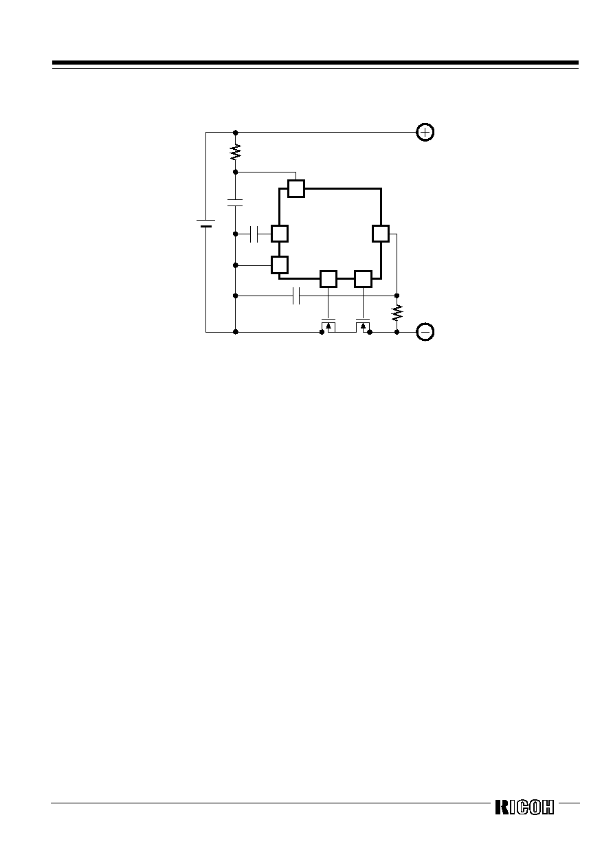
BLOCK DIAGRAM
R5421NxxxC
Level
Shifter
Short circuit
Detector
Delay
5
6
1
3
V
DD
V
SS
D
OUT
C
OUT
V-
4
Ct
VD1
VD2
VD3
2
R5421NxxxF
Level
Shifter
Short circuit
Detector
Delay
5
6
1
3
V
DD
V
SS
D
OUT
C
OUT
V-
4
Ct
VD1
VD2
VD3
2
Rev.1.11
- 3 -
s
SELECTION GUIDE
In the R5421Nxxxx Series three of the input threshold for over-charge, over-discharge and excess current detectors can be
designated.
Part Number is designated as follows:
R5421N XXXX-XX
Part Number
a
b
c
Code
Description
a
Serial Number for the R5421N Series designating input threshold for over-charge, over-discharge
and excess current detectors as well as hysteresis range for over-charge detector.
b
Designation of version symbols
c
Taping Type: TR (refer to Taping Specification)
s
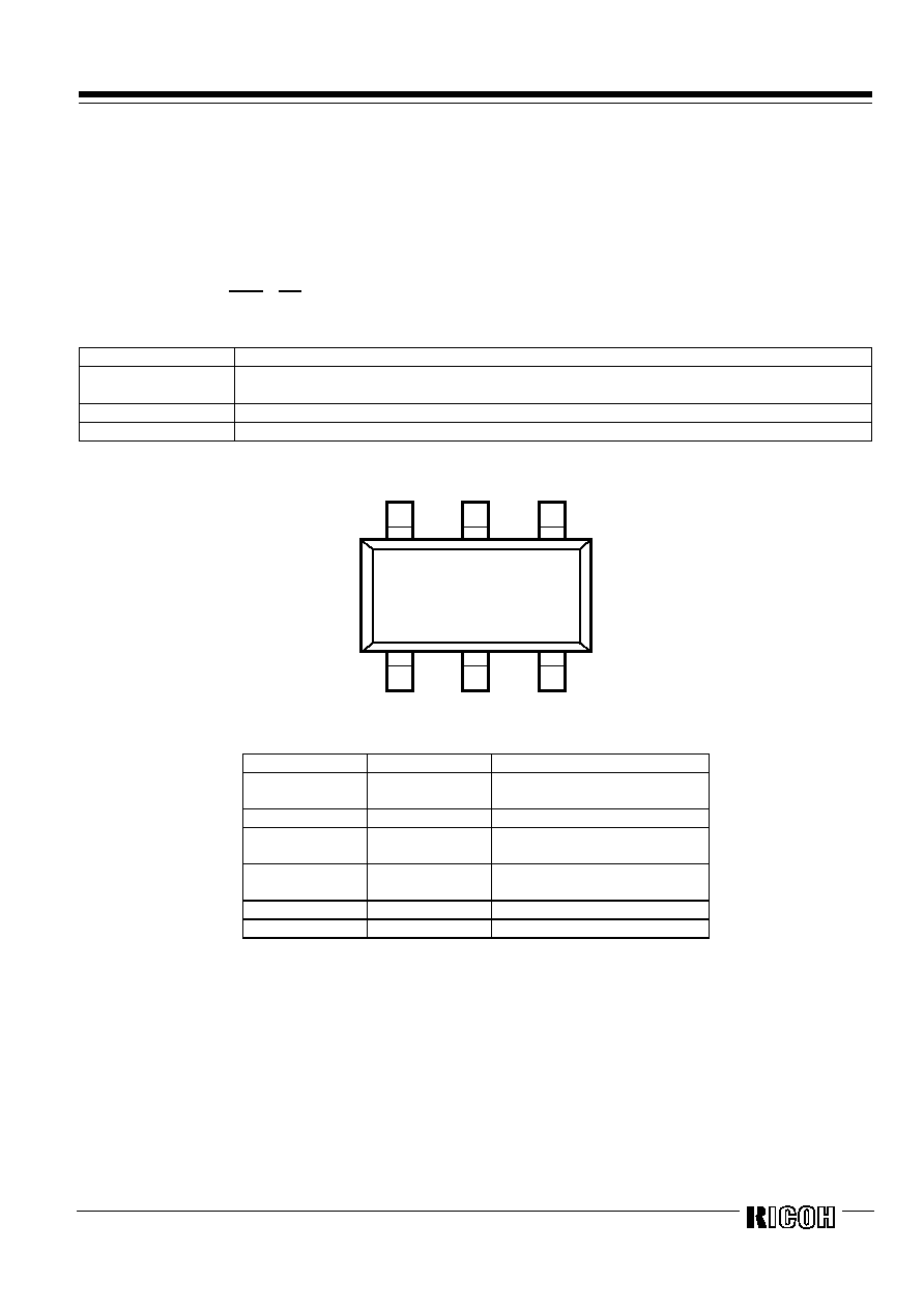
PIN CONFIGURATION
6
5
4
(mark side)
1
2
3
s
PIN DESCRIPTION
Pin No.
Symbol
Pin description
1
D
OUT
Output of over-discharge
detection, CMOS output
2
V-
Pin for charger negative input
3
C
OUT
Output of over-charge
detection, CMOS output
4
Ct
Pin for external capacitor
setting output delay of VD1
5
V
DD
Power supply
6
V
SS
Ground
Rev.1.11
- 4 -
s
ABSOLUTE MAXIMUM RATINGS
V
SS
=0V
Symbol
Item
Ratings
Unit
V
DD
Supply voltage
-0.3 to 12
V
V-
VCt
Input Voltage
V - pin
Ct pin
V
DD
-28 to V
DD
+0.3
V
SS
-0.3 to V
DD
+0.3
V
V
VC
OUT
VD
OUT
Output voltage
C
OUT
pin
D
OUT
pin
V
DD
-28 to V
DD
+0.3
V
SS
-0.3 to V
DD
+0.3
V
V
P
D
Power dissipation
150
mW
Topt
Operating temperature
range
-40 to 85
�C
Tstg
Storage temperature range
-55 to 125
�C
ABSOLUTE MAXIMUM RATINGS
Absolute Maximum ratings are threshold limit values that must not be exceeded ever for an instant under any conditions.
Moreover, such values for any two items must not be reached simultaneously. Operation above these absolute maximum
ratings may cause degradation or permanent damage to the device. These are stress ratings only and do not necessarily
imply functional operation below these limits.
Rev.1.11
- 5 -
s
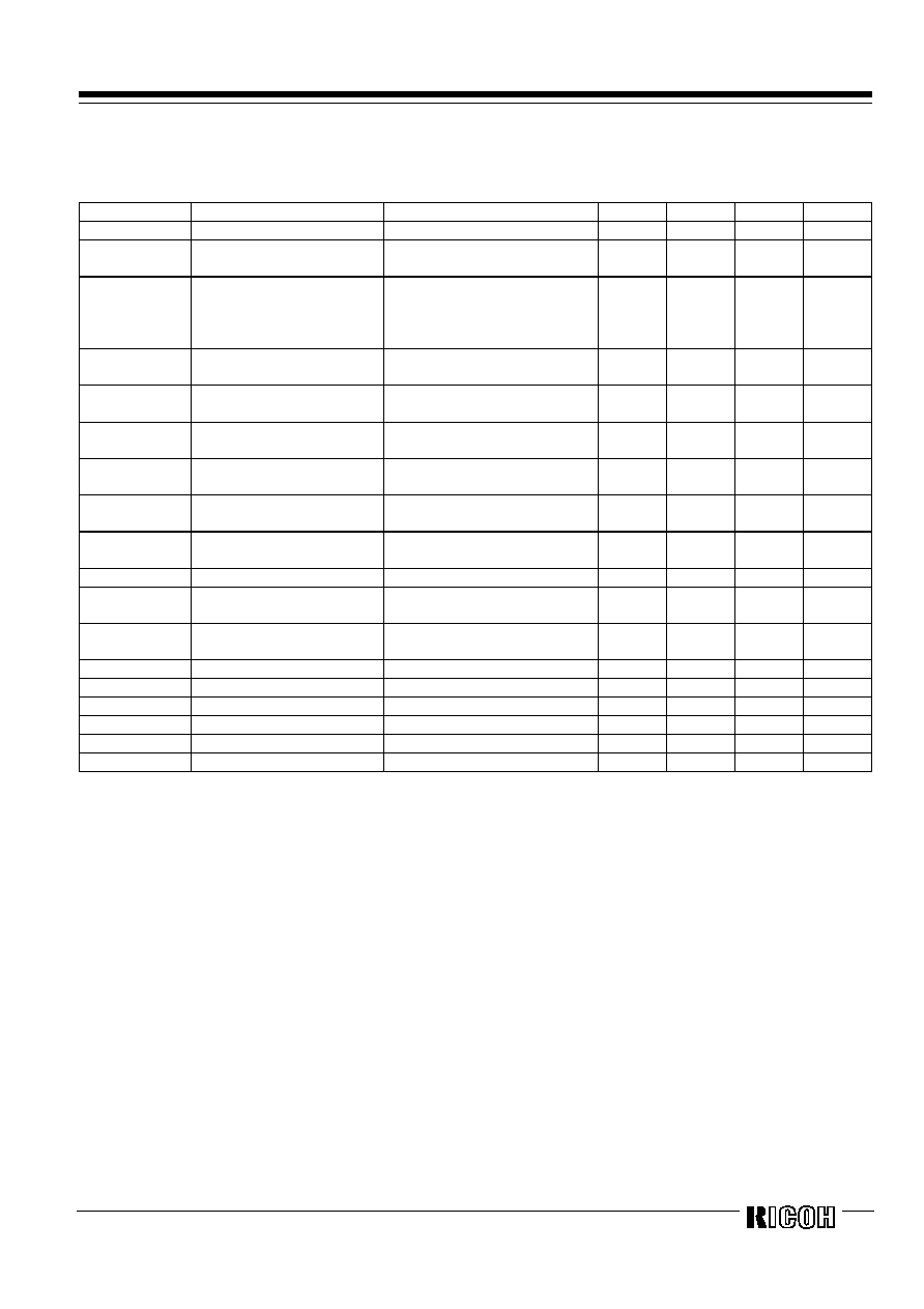
ELECTRICAL CHARACTERISTIC
q
R5421N111C
Topt=25�C
Symbol
Item
Conditions
MIN.
TYP.
MAX.
Unit
V
DD1
Operating input voltage
Voltage defined as V
DD
- V
SS
1.5
10
V
Vst
Minimum operating
Voltage for 0V charging
Voltage defined as V
DD
- V- ,
V
DD
- V
SS
=0V
1.2
V
V
DET1
Over-charge threshold
Detect rising edge of supply
voltage
(Topt=25�C)
(Topt=0 to 50�C)
*Note
4.225
4.220
4.250
4.250
4.275
4.280
V
V
V
REL1
Release voltage for over-
charge detection
4.00
4.05
4.10
V
tV
DET1
Output delay of over-
Charge
C3=0.01�F, V
DD
=3.6V to 4.3V
60
75
90
ms
V
DET2
Over-discharge threshold
Detect falling edge of supply
voltage
2.437
2.500
2.563
V
tV
DET2
Output delay of over-
Discharge
V
DD
=3.6V to 2.4V
7
10
13
ms
V
DET3
Excess current threshold
Detect rising edge of 'V-' pin
voltage
0.17
0.20
0.23
V
tV
DET3
Output delay of excess
Current
V
DD
=3.0V
9
13
17
ms
Vshort
Short protection voltage
V
DD
=3.0V
V
DD
-1.2
V
DD
-0.9
V
DD
-0.6
V
tshort
Output Delay of Short
protection
V
DD
=3.0V
5
50
�s
Rshort
Reset resistance for Excess
current protection
V
DD
=3.6V, V- =1.0V
50
100
150
k
Vol1
Nch ON voltage of C
OUT
Iol=50�A, V
DD
=4.4V
0.35
0.5
V
Voh1
Pch ON voltage of C
OUT
Ioh=-50�A, V
DD
=3.9V
3.4
3.7
V
Vol2
Nch ON voltage of D
OUT
Iol=50�A, V
DD
=2.4V
0.2
0.5
V
Voh2
Pch ON voltage of D
OUT
Ioh=-50�A, V
DD
=3.9V
3.4
3.7
V
I
DD
Supply current
V
DD
=3.9V, V- =0V
3.0
6.0
�A
Istandby
Standby current
V
DD
=2.0V
0.3
0.6
�A
*Note: Considering of variation in process parameters, we compensate for this characteristic related to temperature by laser-
trim, however, this specification is guaranteed by design, not production tested.

Rev.1.11
- 6 -
q
R5421N112C
Topt=25�C
Symbol
Item
Conditions
MIN.
TYP.
MAX.
Unit
V
DD1
Operating input voltage
Voltage defined as V
DD
- V
SS
1.5
10
V
Vst
Minimum operating
Voltage for 0V charging
Voltage defined as V
DD
- V- ,
V
DD
- V
SS
=0V
1.2
V
V
DET1
Over-charge threshold
Detect rising edge of supply
Voltage
Topt=25�C
Topt=0 to 50�C
*Note
4.325
4.320
4.350
4.350
4.375
4.380
V
V
V
REL1
Release voltage for over-
charge detection
4.100
4.150
4.200
V
tV
DET1
Output delay of over-
Charge
C3=0.01�F, V
DD
=3.6V to 4.4V
61
77
93
ms
V
DET2
Over-discharge threshold
Detect falling edge of supply
Voltage
2.437
2.500
2.563
V
tV
DET2
Output delay of over-
Discharge
V
DD
=3.6V to 2.4V
7
10
13
ms
V
DET3
Excess current threshold
Detect rising edge of 'V-' pin
Voltage
0.17
0.20
0.23
V
tV
DET3
Output delay of excess
Current
V
DD
=3.0V
9
13
17
ms
Vshort
Short protection voltage
V
DD
=3.0V
V
DD
-1.2
V
DD
-0.9
V
DD
-0.6
V
tshort
Output Delay of Short
protection
V
DD
=3.0V
5
50
�s
Rshort
Reset resistance for excess
current protection
V
DD
=3.6V, V- =1.0V
50
100
150
k
Vol1
Nch ON voltage of C
OUT
Iol=50�A, V
DD
=4.4V
0.35
0.5
V
Voh1
Pch ON voltage of C
OUT
Ioh=-50�A, V
DD
=3.9V
3.4
3.7
V
Vol2
Nch ON voltage of D
OUT
Iol=50�A, V
DD
=2.4V
0.2
0.5
V
Voh2
Pch ON voltage of D
OUT
Ioh=-50�A, V
DD
=3.9V
3.4
3.7
V
I
DD
Supply current
V
DD
=3.9V,V- =0V
3.0
6.0
�A
Istandby
Standby current
V
DD
=2.0V
0.3
0.6
�A
*Note: Considering of variation in process parameters, we compensate for this characteristic related to temperature by laser-
trim, however this specification is guaranteed by design, not production tested.

Rev.1.11
- 7 -
q
R5421N151F
Topt=25�C
Symbol
Item
Conditions
MIN.
TYP.
MAX.
Unit
V
DD1
Operating input voltage
Voltage defined as V
DD
- V
SS
1.5
10
V
Vst
Minimum operating
Voltage for 0V charging
Voltage defined as V
DD
- V- ,
V
DD
- V
SS
=0V
1.2
V
V
DET1
Over-charge threshold
Detect rising edge of supply
Voltage
Topt=25�C
Topt=0 to 50�C
*Note
4.225
4.220
4.250
4.250
4.275
4.280
V
V
V
REL1
Release voltage for over-
charge detection
4.000
4.050
4.100
V
tV
DET1
Output delay of over-
Charge
C3=0.01�F, V
DD
=3.6V to 4.3V
60
75
90
ms
V
DET2
Over-discharge threshold
Detect falling edge of supply
Voltage
2.437
2.500
2.563
V
tV
DET2
Output delay of over-
Discharge
V
DD
=3.6V to 2.4V
7
10
13
ms
V
DET3
Excess current threshold
Detect rising edge of 'V-' pin
Voltage
0.17
0.20
0.23
V
tV
DET3
Output delay of excess
Current
V
DD
=3.0V
9
13
17
ms
Vshort
Short protection voltage
V
DD
=3.0V
V
DD
-1.2
V
DD
-0.9
V
DD
-0.6
V
tshort
Output Delay of Short
protection
V
DD
=3.0V
5
50
�s
Rshort
Reset resistance for excess
current protection
V
DD
=3.6V, V- =1.0V
50
100
150
k
Vol1
Nch ON voltage of C
OUT
Iol=50�A, V
DD
=4.4V
0.35
0.5
V
Voh1
Pch ON voltage of C
OUT
Ioh=-50�A, V
DD
=3.9V
3.4
3.7
V
Vol2
Nch ON voltage of D
OUT
Iol=50�A, V
DD
=2.2V
0.2
0.5
V
Voh2
Pch ON voltage of D
OUT
Ioh=-50�A, V
DD
=3.9V
3.4
3.7
V
I
DD
Supply current
V
DD
=3.9V,V- =0V
3.0
6.0
�A
Istandby
Standby current
V
DD
=2.0V
1.0
2.0
�A
*Note: Considering of variation in process parameters, we compensate for this characteristic related to temperature by laser-
trim, however, this specification is guaranteed by design, not production tested.
Rev.1.11
- 8 -
q
R5421N152F
Topt=25�C
Symbol
Item
Conditions
MIN.
TYP.
MAX.
Unit
V
DD1
Operating input voltage
Voltage defined as V
DD
- V
SS
1.5
10
V
Vst
Minimum operating
Voltage for 0V charging
Voltage defined as V
DD
- V- ,
V
DD
- V
SS
=0V
1.2
V
V
DET1
Over-charge threshold
Detect rising edge of supply
Voltage
Topt=25�C
Topt=0 to 50�C
*Note
4.325
4.320
4.350
4.350
4.375
4.380
V
V
V
REL1
Release voltage for over-
charge detection
4.100
4.150
4.200
V
tV
DET1
Output delay of over-
Charge
C3=0.01�F, V
DD
=3.6V to 4.4V
61
77
93
ms
V
DET2
Over-discharge threshold
Detect falling edge of supply
Voltage
2.437
2.500
2.563
V
tV
DET2
Output delay of over-
Discharge
V
DD
=3.6V to 2.4V
7
10
13
ms
V
DET3
Excess current threshold
Detect rising edge of 'V-' pin
Voltage
0.17
0.20
0.23
V
tV
DET3
Output delay of excess
Current
V
DD
=3.0V
9
13
17
ms
Vshort
Short protection voltage
V
DD
=3.0V
V
DD
-1.2
V
DD
-0.9
V
DD
-0.6
V
tshort
Output Delay of Short
protection
V
DD
=3.0V
5
50
�s
Rshort
Reset resistance for excess
current protection
V
DD
=3.6V, V- =1.0V
50
100
150
k
Vol1
Nch ON voltage of C
OUT
Iol=50�A, V
DD
=4.4V
0.35
0.5
V
Voh1
Pch ON voltage of C
OUT
Ioh=-50�A, V
DD
=3.9V
3.4
3.7
V
Vol2
Nch ON voltage of D
OUT
Iol=50�A, V
DD
=2.2V
0.2
0.5
V
Voh2
Pch ON voltage of D
OUT
Ioh=-50�A, V
DD
=3.9V
3.4
3.7
V
I
DD
Supply current
V
DD
=3.9V,V- =0V
3.0
6.0
�A
Istandby
Standby current
V
DD
=2.0V
1.0
2.0
�A
*Note: Considering of variation in process parameters, we compensate for this characteristic related to temperature by laser-
trim, however, this specification is guaranteed by design, not production tested.

Rev.1.11
- 9 -
s
OPERATION
q
VD1 / Over-Charge Detector in the 'C' version
The VD1 monitors V
DD
pin voltage. When the V
DD
voltage crosses over-charge detector threshold V
DET1
from a low value to
a value higher than the V
DET1
, the VD1 can sense a over-charging and an external charge control Nch-MOS-FET turns to
"OFF" with C
OUT
pin being at "Low" level.
There can be two cases to reset the VD1 making the C
OUT
pin level to "High" again after detecting over-charge. Resetting
the VD1 can make charging system allowable to resumption of charging process.
The first case is in such conditions that a time when the V
DD
voltage is coming down to a level lower than "V
REL1
".
While in the second case, connecting a kind of loading to V
DD
after disconnecting a charger from the battery pack can make
the VD1 resetting when the V
DD
level is in between "V
DET1
" and "V
REL1"
.
After detecting over-charge with the V
DD
voltage of higher than V
DET1
, connecting system load to the battery pack makes
load current allowable through parasitic diode of external charge control FET.
The C
OUT
level would be High when the V
DD
level is coming down to a level below the V
DET1
by continuous drawing of load
current.
An output delay time for over-charge detection can be set by external capacitor C3 connecting between the V
SS
pin and Ct
pin. The external capacitor can make a delay time from a moment detecting over-charge to a time output a signal which
enables charge control FET turn to "OFF".
When the V
DD
level is going up to a higher level than V
DET1
if the V
DD
voltage would be back to a level lower than the V
DET1
within a time period of the output delay time, VD1 would not output a signal for turning "OFF" of charge control FET.
The output delay time can be calculated as below:
tV
DET1
[sec] = (C3[F]
�
(V
DD
[V]-0.7) / (0.48
�
10
-6
)
Note:Topt=25�C V
DD
value should be after over-charge detection.
A level shifter incorporated in a buffer driver for the C
OUT
pin makes the "Low" level of C
OUT
pin to the V - pin voltage and
the "High" level of C
OUT
pin is set to V
DD
voltage with CMOS buffer.
q
VD2 / Over-Discharge Detector
The VD2 is monitoring a V
DD
pin voltage. When the V
DD
voltage crosses the over-discharge detector threshold V
DET2
from a
high value to a value lower than the V
DET2
, the VD2 can sense an over-discharging and the external discharge control Nch
MOS FET turns to "OFF" with the D
OUT
pin being at "Low" level.
To reset the VD2 with the D
OUT
pin level being "H" again after detecting over-discharge it is necessary to connect a charger
to the battery pack for R5421NxxxC. When the V
DD
voltage stays under over- discharge detector threshold V
DET2
charge
current can flow through parasitic diode of external discharge control MOS FET, then after the V
DD
voltage comes up to a
value larger than V
DET2,
D
OUT
becomes "H" and discharging process would be able to advance through ON state MOS FET
for discharge control.
Connecting a charger to the battery pack makes the D
OUT
level being "H" instantaneously when the V
DD
voltage is higher
than V
DET2
.
Besides, for R5421NxxxF, when a cell voltage reaches equal or more than over-discharge released voltage, or V
REL2
, over-
discharge condition can be also released
When a cell voltage equals to zero, connecting charger to the battery pack makes the system allowable to charge with higher
charge voltage than Vst, 1.2V Max.
An output delay time for the over-discharge detection is fixed internally, tV
DET2
=10ms typ. at V
DD
=2.4V. When the V
DD
level
is going down to a lower level than V
DET2
if the V
DD
voltage would be back to a level higher than the V
DET2
within a time
period of the output delay time, VD2 would not output a signal for turning "OFF" of discharge control FET.
After detection of an over-discharge by VD2, supply current would be reduced to typically 0.3�A(for R5421NxxxC) or
1.0
�
A(for R5421NxxxF) at V
DD
=2.0V and into standby, only the charger detector is operating.
The output type of D
OUT
pin is CMOS having "H" level of V
DD
and "L" level of V
SS
.

Rev.1.11
- 10 -
q
VD3/Excess Current Detector, Short Circuit Protector
Both of the excess current detector and short circuit protector can work when both control FETs are in "ON" state.
When the V- pin voltage is going up to a value between the short protection voltage Vshort /V
DD
and excess current
threshold V
DET3
, the excess current detector operates and further soaring of V- pin voltage higher than Vshort makes the
short circuit protector enabled. This leads the external discharge control Nch MOS FET turns to "OFF" with the D
OUT
pin
being at "Low" level.
An output delay time for the excess current detector is internally fixed, 13ms typ. at V
DD
=3.0V.
A quick recovery of V- pin level from a value between Vshort and V
DET3
within the delay time keeps the discharge control
FET staying "High" state.
When the short circuit protector is enabled ,the D
OUT
would be Low and its delay time would be 5�s typ.
The V - pin has a built-in pulled down resistor ,typ.100k
, with connecting to the V
SS
pin.
After an excess current or short circuit protection is detected, removing a cause of excess current or external short circuit
makes an external discharge control FET to an "ON" state automatically with the V- pin level being down to the V
SS
level
through pulled down resistor built-in internally.
If V
DD
voltage would be higher than V
DET2
at a time when the excess current is detected the R5421NxxxC does not enter a
standby mode, or otherwise in case of lower V
DD
voltage than V
DET2
would lead the R5421NxxxC into a standby.
After detecting short circuit the R5421NxxxC will not enter a standby mode.
Rev.1.11
- 11 -
s
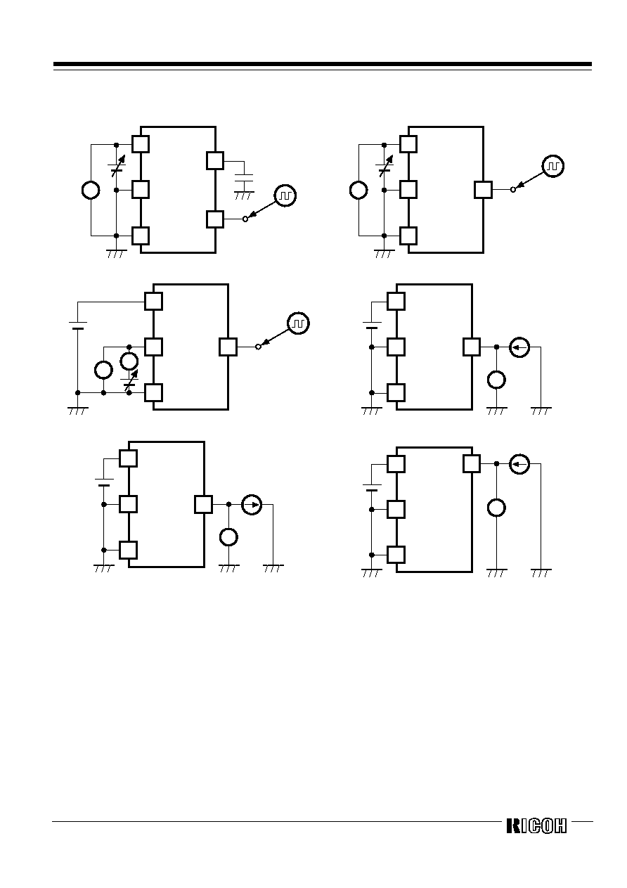
TEST CIRCUITS
5
2
V
6
4
3
0.01
�
F
5
2
V
6
1
Test Circuit 1
Test Circuit 2
5
2
V
A
6
1
5
2
V
6
3
50
�
A
Test Circuit 3
Test Circuit 4
5
2
V
6
3
50
�
A
5
2
V
6
1
50
�
A
Test Circuit 5
Test Circuit 6

Rev.1.11
- 12 -
5
2
V
6
1
50
�
A
5
2
A
6
Test Circuit 7
Test Circuit 8
C3
5
2
C1
R1
V
6
1
3
5
2
C2
R2
V
6
1
Test Circuit 9
Test Circuit 10
The typical characteristics were obtained by use of these test circuits.
Test Circuit 1
: Typical Characteristics 1) 5) 7) 17)
Test Circuit 2
: Typical Characteristics 2) 6) 8)
Test Circuit 3
: Typical Characteristics 3) 4) 9) 10) 19)
Test Circuit 4
: Typical Characteristics 13)
Test Circuit 5
: Typical Characteristics 14)
Test Circuit 6
: Typical Characteristics 15)
Test Circuit 7
: Typical Characteristics 16)
Test Circuit 8
: Typical Characteristics 11) 12)
Test Circuit 9
: Typical Characteristics 21)
Test Circuit 10
: Typical Characteristics 18) 20)
Rev.1.11
- 13 -
s
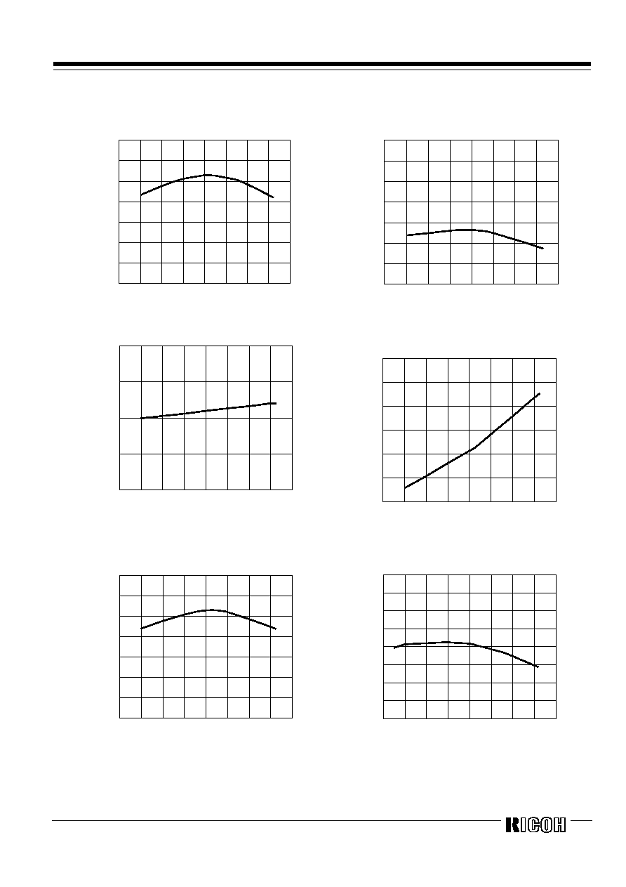
TYPICAL CHARACTERISTICS
1)
Over-charge Threshold vs. Temperature
2)
Over-discharge Threshold vs. Temperature
4.200
4.210
4.220
4.230
4.240
4.250
4.260
4.270
Temperature Topt (
�
C)
60
40
-40
-20
0
100
80
20
-60
Ov
er-charge Threshold V
DET1
(V)
2.470
2.480
2.490
2.500
2.510
2.520
2.530
2.540
Temperature Topt (
�
C)
60
40
-40
-20
0
100
80
20
-60
Ov
er-discharge Threshold V
DET2
(V)
3)
Excess Current Threshold vs. Temperature
4)
Short Circuit Protector Threshold vs. Temperature
0.190
0.195
0.200
0.205
0.210
Temperature Topt (
�
C)
60
40
-40
-20
0
100
80
20
-60
Excess
Current Threshold V
DET3
(V)
2.10
2.15
2.20
2.25
2.35
2.30
2.40
Temperature Topt (
�
C)
60
40
-40
-20
0
100
80
20
-60
Shor
t Circuit Protector
Threshold
Vshor
t (V)
V
DD
=3.0(V)
5)
Over-charge Released Voltage vs. Temperature
6)
Over-discharge Released Voltage vs. Temperature
(for R5421NxxxF)
4.000
4.010
4.020
4.030
4.040
4.050
4.060
4.070
Temperature Topt (
�
C)
60
40
-40
-20
0
100
80
20
-60
Ov
er-charge
Released V
oltage V
REL1
(V)
3.06
3.07
3.08
3.09
3.1
3.11
3.12
3.14
3.13
60
40
-40
-20
0
100
80
20
-60
Temperature Topt (
�
C)
Ov
er-charge
Released V
oltage V
REL2
(V)
Rev.1.11
- 14 -
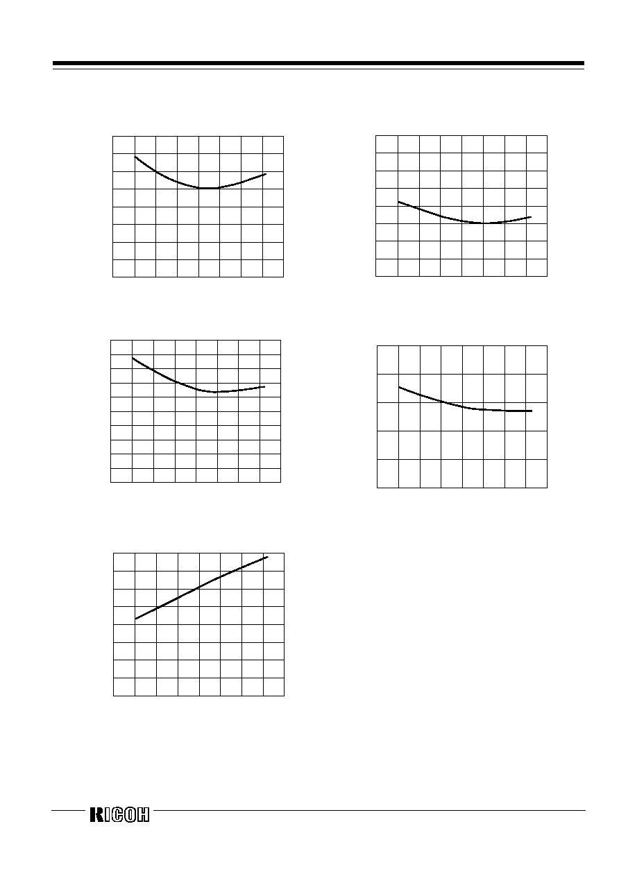
7)
Output Delay of Over-charge vs. Temperature
8)
Output Delay of Over-discharge vs. Temperature
20
30
40
50
60
70
80
90
100
C=0.01(
�
F) V
DD
=3.6(V)
4.3(V)
Temperature Topt (
�
C)
60
40
-40
-20
0
100
80
20
-60
Output Dela
y of Ov
er-charge tV
DET1
(ms)
2
4
6
8
10
12
14
16
18
V
DD
=3.6(V)
2.2(V)
Temperature Topt (
�
C)
60
40
-40
-20
0
100
80
20
-60
Output Dela
y of Ov
er-discharge tV
DET2
(ms)
9)
Output delay of Excess current vs. Temperature
10) Output Delay of Short circuit protector vs. Temperature
0
2
4
6
8
10
12
14
20
18
16
V
DD
=3.0(V)
Temperature Topt (
�
C)
60
40
-40
-20
0
100
80
20
-60
Output Dela
y of Excess Current tV
DET3
(ms)
0
2
4
6
10
8
V
DD
=3.0(V)
Temperature Topt (
�
C)
60
40
-40
-20
0
100
80
20
-60
Output Dela
y of Shor
t Circuit Protector tVshor
t (
�
s)
11) Supply Current vs. Temperature
0.0
0.5
1.0
1.5
2.0
2.5
3.0
3.5
4.0
V
DD
=3.9(V) V-=0(V)
Temperature Topt (
�
C)
60
40
-40
-20
0
100
80
20
-60
Supply Current I
DD
(
�
A)

Rev.1.11
- 15 -
12) Supply Current vs. Temperature(for R5421NxxxC)
12) Standby Current vs. Temperature(for R5421NxxxF)
Standb
y Current Istandb
y (
�
A)
0.00
0.05
0.10
0.15
0.20
0.25
0.30
0.35
0.40
V
DD
=2.0(V)
Temperature Topt (
�
C)
60
40
-40
-20
0
100
80
20
-60
0
0.6
0.4
0.6
0.8
1
1.2
1.4
V
DD
=2.0(V)
60
40
-40
-20
0
100
80
20
-60
Standb
y Current Istandb
y (
�
A)
Temperature Topt (
�
C)
13) C
OUT
Nch Driver ON Voltage vs. Temperature
14) C
OUT
Pch Driver ON Voltage vs. Temperature
I
OL
= 50(
�
A) V
DD
=4.4(V)
0.300
0.350
0.400
0.250
0.150
0.200
0.100
Temperature Topt (
�
C)
-60
-40
20
40
60
80
100
-20
0
C
OUT
Nch Dr
iv
er ON
V
oltage
V
OL1
(V)
I
CH
= 50(
�
A) V
DD
=3.9(V)
3.800
3.850
3.900
3.750
3.650
3.700
3.600
Temperature Topt (
�
C)
-60
-40
20
40
60
80
100
-20
0
C
OUT
Pch Dr
iv
er ON
V
oltage V
OH1
(V)
15) D
OUT
Nch Driver ON Voltage vs. Temperature
16) D
OUT
Pch Driver ON Voltage vs. Temperature
I
OL
= 50(
�
A) V
DD
=2.4(V)
0.350
0.400
0.450
0.500
0.300
0.250
0.100
0.150
0.200
0.050
Temperature Topt (
�
C)
-60
-40
20
40
60
80
100
-20
0
D
OUT
Nch Dr
iv
er ON
V
oltage V
OL2
(V)
I
CH
= 50(
�
A) V
DD
=3.9(V)
3.800
3.850
3.900
3.750
3.650
3.700
3.600
-60
-40
20
40
60
80
100
-20
0
D
OUT
Pch Dr
iv
er ON
V
oltage
V
OH2
(V)
Temperature Topt (
�
C)
Rev.1.11
- 16 -
17) Output Delay of Over-charge vs. Capacitance C3
18) Output Delay of Short protection vs. Capacitance C2
V
DD
=3.8V
4.3V(R1=100
, C1=0.1
�
F, R2=1k
, C2=0.1
�
F)
1.4
1.2
1
1.8
1.6
2
0.8
0.6
0.2
0.4
0
C3 (
�
F)
0
0.1
0.05
0.2
0.25
0.15
Output Dela
y of Ov
er-charge (s)
10000
1000
100
10
1
C2 (
�
F)
R1=100
, C1=0.1
�
F, C3=0.01
�
F, R2=1k
0.001
0.1
0.01
1
Output Dela
y of Shor
t Protection (
�
s)
19) Output Delay of Excess Current vs. V
DD
20) Excess Current Threshold vs. External Resistance R2
0
5
10
15
25
20
V-=0V
1V
Supply Voltage V
DD
(V)
4
3
4.5
3.5
2.5
Output Dela
y
Time of Excess Current tV
DET3
(ms)
0.19
0.20
0.21
0.23
0.22
R2 (k
)
2
0.5
1
3
2.5
1.5
0
Excess
Current Threshold V
DET3
(V)
21) Over-charge Threshold vs. External Resistance R1
R1 (
)
Ov
er-chag
re Threshold
(V)
4.264
4.266
4.268
4.27
4.274
4.272
600
200
400
1000
800
0
Rev.1.11
- 17 -
s
TYPICAL APPLICATION
R5421NxxxC
2
4
6
1
5
3
R1
100
R2
1k
C3
0.01
�
F
C2
0.1
�
F
C1
0.1
�
F
s
APPLICATION HINTS
R1 and C1 will stabilize a supply voltage to the R5421NxxxC. A recommended R1 value is less than 1k
.
A larger value of R1 leads higher detection voltage, makes some errors, because of shoot through current flowed in the
R5421NxxxC.
R2 and C2 will stabilize a V- pin voltage. The resetting from over-discharge with connecting a charger possibly be disabled by
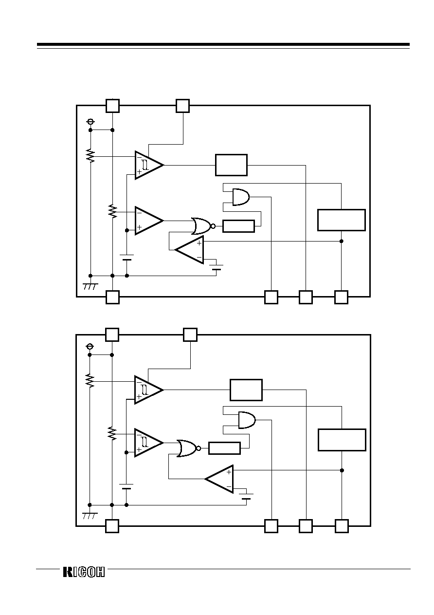
larger value of R2. Recommended value is less than 1 k
.
After an over-charge detection even connecting battery pack to a system probably could not allow a system to draw load
current by a larger R2C2 time constant in the C version.
Recommended C2 value is less than 1�F.
R1 and R2 can operate also as a part of current limit circuit against for setting cell reverse direction or for applying excess
charging voltage to the R5421NxxxC, battery pack, while smaller
R1 and R2 may cause a power consumption over rating of power dissipation of the R5421NxxxC and a total of 'R1+R2' should
be more than 1k
.
The time constants R1C1 or R2C2 must have a relations as below:
R1C1
R2C2
Because in case that R1C1, time constant for V
DD
pin ,would be larger than R2C2, time constant for V- pin, then the
R5421NxxxC might be into a standby mode after detecting excess current or short circuit current.
Rev.1.11
- 18 -
s
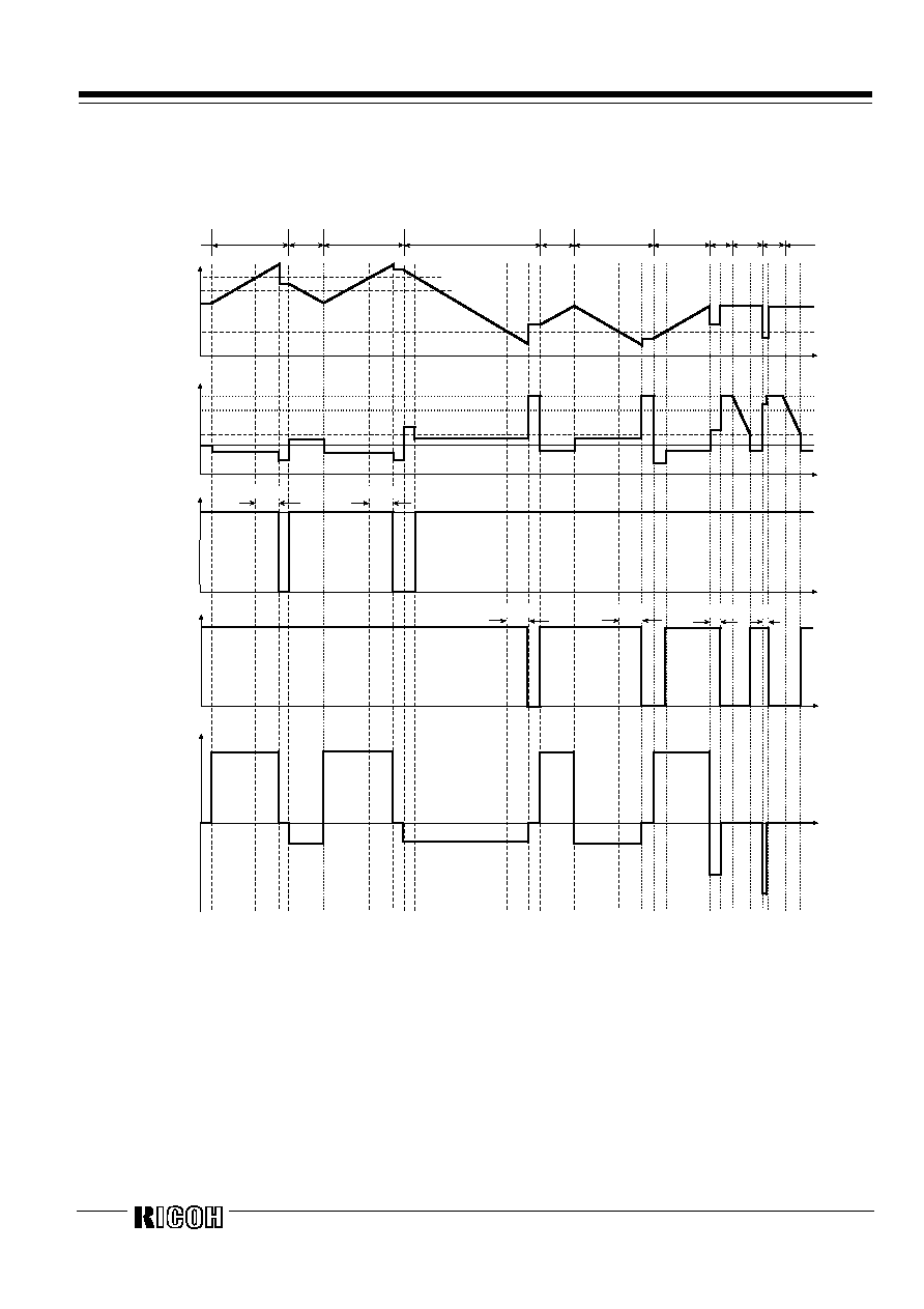
TIMING DIAGRAM
q
R5421NXXXC
t
t
t
t
t
V
DET
V
DET
Vshort
V
DET3
V
DD
V
DD
V
DD
V-
V-
C
OUT
D
OUT
V
DD
V
SS
V
SS
V
REL1
0
tV
DET1
tV
DET1
tV
DET2
tV
DET2
tV
DET3
tshort
Excess
current
Short
circuit
Open
Open
Charging
Current
Discharging
Current
Charging
Charging
Charging
Charging
Discharging
Discharging
Discharging
Rev.1.11
- 19 -
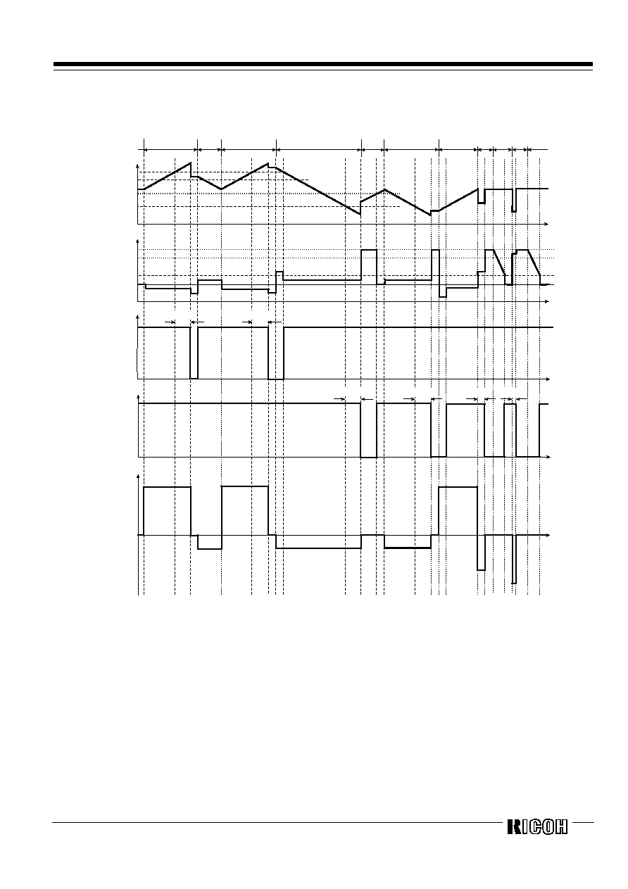
q
R5421NXXXF
t
t
t
t
t
V
DET1
V
DET
Vshort
V
DET3
V
DD
V
DD
V-
V-
D
OUT
C
OUT
V
DD
V
DD
V
SS
V
SS
V
REL1
V
REL2
0
tV
DET1
tV
DET1
tV
DET2
tV
DET2
tV
DET3
tshort
Charging
Charging
Charging
Discharging
Discharging
Discharging
Open
Short
circuit
Excess
current
Open
Open
Charging
Current
Discharging
Current