
'99.12.9
PRELIMINARY
Li-Ion BATTERY PROTECTOR
R5422NxxxC/xxxE series
Rev. 0.01
- 1 -
n
OUTLINE
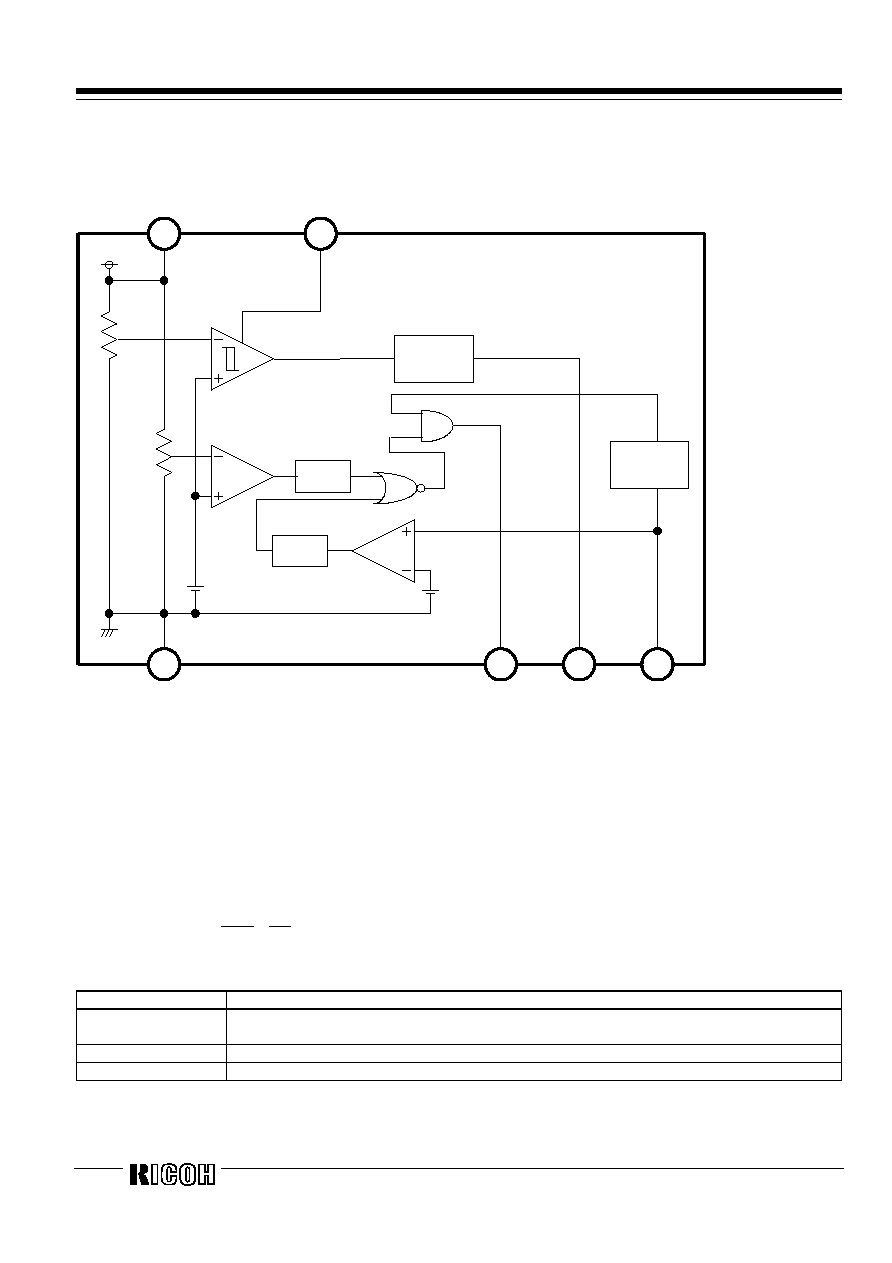
The R5422NxxxC/E Series are protection ICs for over-charge/discharge of rechargeable one-cell Lithium-ion (Li+) excess load
current, further include a short circuit protector for preventing large external short circuit current.
Each of these ICs is composed of three voltage detectors, a reference unit, a delay circuit, a short circuit protector, and a logic
circuit. When charging voltage crosses the detector threshold from a low value to a value higher than V
DET1
, the output of C
OUT
pin, the output of over-charge detector/VD1, switches to low level, charger's negative pin level after the delay time by setting an
external capacitor. After detecting over-charge the VD1 can be reset and the output of C
OUT
becomes high when the V
DD
voltage
is coming down to a level lower than "V
REL1
", or when a kind of loading is connected to V
DD
after a charger is disconnected from
the battery pack while the V
DD
level is in between "V
DET1
" and "V
REL1
" in the R5422NxxxC/E version.
The output of D
OUT
pin, the output of over-discharge detector/VD2, switches to low level after internally fixed delay time passed,
when discharging voltage crosses the detector threshold from a high value to a value lower than V
DET2
.
After R5422NxxxC/E Series detect the over-discharge voltage, connect a charger to the battery pack, and when the battery
supply voltage becomes higher than the over-discharge detector threshold, VD2 is released and the voltage of D
OUT
becomes
"H" level.
An excess load current can be sensed and cut off after internally fixed delay time passed through the built in excess current
detector, VD3, with D
OUT
being enabled to low level. Once after detecting excess current, the VD3 is released and D
OUT
level
switches to high by detaching a battery pack from a load system.
Further, short circuit protector makes D
OUT
level to low immediately with external short circuit current and removing external
short circuit leads D
OUT
level to high. After detecting over-discharge, supply current will be kept extremely low by halt some
internal circuits operation. Output type of C
OUT
and D
OUT
is CMOS. 6-pin, SOT23-6 is available.
n
FEATURES
l
High Voltage Process Technology Absolute Maximum Rating of Voltage level between V
DD
-V- 28v
l
Low supply current....................................................Supply current
Typ. 6.0µA
Standby current (detecting over-discharge)
Typ. 0.1µA
l
High accuracy detector threshold ..............................Over-charge detector (Topt=25∞C)
±25mV
(Topt=0 to 50∞C)
±30 mV
Over-discharge detector
±2.5%
Excess current detector
±20mV
l
Variety of detector threshold .....................................Over-charge detector threshold
4.0V - 4.5V step of 0.01V
Over-discharge detector threshold
2.0V - 3.0V step of 0.01V
l
Built-in protection circuit ..........................................Excess current protection
0.05V - 0.4V step of 0.01V
l
Output delay of over-charge ......................................Time delay at C=0.01µF tV
DET1
=75ms, tV
REL1
=20ms
l
Output delay of over-discharge .................................Internally fixed TYP. 17ms
l
Output delay of excess-current Internally fixed TYP. 10ms
l
2 Over-current modes Excess Current Mode / Short Mode
l
Charging Available / non-available at 0V Cell Acceptable of 0V Cell C version
Non-acceptable of 0V Cell E versi on
l
Small package............................................................SOT-23-6 / 6-pin
n
APPLICATIONS
l
Li+ one-cell protector for battery pack
Rev. 0.01
- 2 -
n
BLOCK DIAGRAM
Short
Detector
Dout
Cout
V-
Vss
2
3
1
Delay
4
Ct
V
DD
VD1
VD2
5
6
Level
Shift
VD3
Delay
n
SELECTION GUIDE
In the R5422Nxxxx Series, three of the input threshold for over-charge, over-discharge and excess current detectors can be
designated.
Part Number is designated as follows:
R5422N XXXX-XX
¨Part Number
- - -
a
b
c
Code
Description
a
Serial Number for the R5422N Series designating input threshold for over-charge, over-discharge
and excess current detectors as well as hysteresis range for over-charge detector.
b
Designation of version symbols
c
Taping Type: TR (refer to Taping Specification)
Rev.0.01
- 3 -
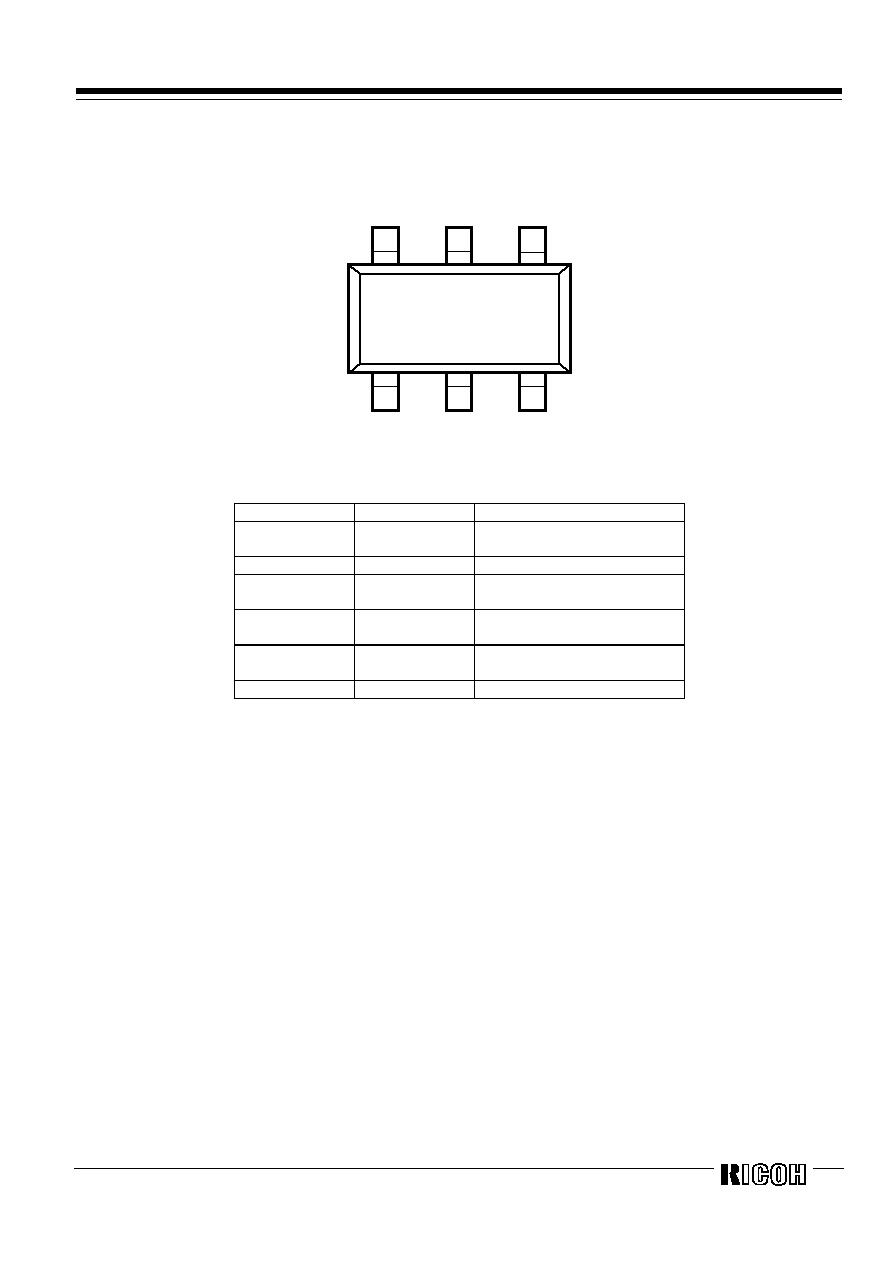
n
PIN CONFIGURATION
6
5
4
(mark side)
1
2
3
n
PIN DESCRIPTION
Pin No.
Symbol
Pin description
1
D
OUT
Output of over-discharge
detection, CMOS output
2
V-
Pin for charger negative input
3
C
OUT
Output of over-charge
detection, CMOS output
4
Ct
Pin for external capacitor
setting output delay of VD1
5
V
DD
Power supply(Substrate voltage
level of the IC)
6
V
SS
Ground(Ground pin of the IC)
Rev. 0.01
- 4 -
n
ABSOLUTE MAXIMUM RATINGS
V
SS
=0V
Symbol
Item
Ratings
Unit
V
DD
Supply voltage
-0.3 to 12
V
V-
VCt
Input Voltage
V - pin
Ct pin
V
DD
-28 to V
DD
+0.3
V
SS
-0.3 to V
DD
+0.3
V
V
VC
OUT
VD
OUT
Output voltage
C
OUT
pin
D
OUT
pin
V
DD
-28 to V
DD
+0.3
V
SS
-0.3 to V
DD
+0.3
V
V
P
D
Power dissipation
150
mW
Topt
Operating temperature
range
-40 to 85
∞C
Tstg
Storage temperature range
-55 to 125
∞C
ABSOLUTE MAXIMUM RATINGS
Absolute Maximum ratings are threshold limit values that must not be exceeded ever for an instant under any conditions.
Moreover, such values for any two items must not be reached simultaneously. Operation above these absolute maximum
ratings may cause degradation or permanent damage to the device. These are stress ratings only and do not necessarily imply
functional operation below these limits.
Rev.0.01
- 5 -
n
ELECTRICAL CHARACTERISTIC
l
R5422N111C
Unless otherwise provided,
Topt=25∞C
Symbol
Item
Conditions
MIN.
TYP.
MAX.
Unit
V
DD1
Operating input voltage
Voltage defined as V
DD
- V
SS
1.5
10
V
Vst
Minimum operating Voltage
for 0V charging
Voltage defined as V
DD
- V- ,
V
DD
- V
SS
=0V
1.2
V
V
DET1
Over-charge threshold
R1=330
W(Topt=25∞C)
R1=330
W (Topt=0 to 50∞C)
*Note
4.225
4.220
4.250
4.250
4.275
4.280
V
V
V
REL1
Release voltage for over-
charge detection
4.000
4.050
4.100
V
tV
DET1
Output delay of over-
Charge
C=0.01µF, V
DD
=3.6V to 4.3V
60
75
90
ms
tV
REL1
Output delay of Release
from Over-charge
C=0.01µF, V
DD
=4.3V to 4.1V
15
20
25
ms
V
DET2
Over-discharge threshold
Detect falling edge of supply
voltage
2.437
2.500
2.563
V
tV
DET2
Output delay of over-
Discharge
V
DD
=3.6V to 2.4V
12
17
22
ms
V
DET3
Excess current threshold
Detect rising edge of 'V-' pin
voltage
0.18
0.20
0.22
V
tV
DET3
Output delay of excess
Current
7
10
13
ms
Vshort
Short protection voltage
V
DD
=3.0V
V
DD
-1.2
V
DD
-0.9
V
DD
-0.6
V
tshort
Output Delay of Short
protection
V
DD
=3.0V
5
50
µs
Rshort
Reset resistance for Excess
current protection
V
DD
=3.6V, V- =1.0V
37
75
113
k
W
Vol1
Nch ON voltage of C
OUT
Iol=40µA, V
DD
=4.4V
0.3
0.5
V
Voh1
Pch ON voltage of C
OUT
Ioh=-40µA, V
DD
=3.9V
3.4
3.75
V
Vol2
Nch ON voltage of D
OUT
Iol=40µA, V
DD
=2.2V
0.2
0.5
V
Voh2
Pch ON voltage of D
OUT
Ioh=-40µA, V
DD
=3.9V
3.4
3.7
V
I
DD
Supply current
V
DD
=3.9V, V- =0V
6.0
10.0
µA
Istandby
Standby current
V
DD
=2.0V
0.1
µA
*Note: Considering of variation in process parameters, we compensate for this characteristic related to temperature by laser-trim,
however, this specification is guaranteed by design, not production tested.

Rev. 0.01
- 6 -
l
R5422N112C
Unless otherwise provided,
Topt=25∞C
Symbol
Item
Conditions
MIN.
TYP.
MAX.
Unit
V
DD1
Operating input voltage
Voltage defined as V
DD
- V
SS
1.5
10
V
Vst
Minimum operating Voltage
for 0V charging
Voltage defined as V
DD
- V- ,
V
DD
- V
SS
=0V
1.2
V
V
DET1
Over-charge threshold
R1=330
W(Topt=25∞C)
R1=330
W (Topt=0 to 50∞C)
*Note
4.325
4.320
4.350
4.350
4.375
4.380
V
V
V
REL1
Release voltage for over-
charge detection
4.100
4.150
4.200
V
tV
DET1
Output delay of over-
Charge
C=0.01µF, V
DD
=3.6V to 4.4V
61
77
93
ms
tV
REL1
Output delay of Release
from Over-charge
C=0.01µF, V
DD
=4.4V to 4.1V
15
20
25
ms
V
DET2
Over-discharge threshold
Detect falling edge of supply
Voltage
2.437
2.500
2.563
V
tV
DET2
Output delay of over-
Discharge
V
DD
=3.6V to 2.4V
12
17
22
ms
V
DET3
Excess current threshold
Detect rising edge of 'V-' pin
Voltage
0.18
0.20
0.22
V
tV
DET3
Output delay of excess
Current
7
10
13
ms
Vshort
Short protection voltage
V
DD
=3.0V
V
DD
-1.2
V
DD
-0.9
V
DD
-0.6
V
tshort
Output Delay of Short
protection
V
DD
=3.0V
5
50
µs
Rshort
Reset resistance for excess
current protection
V
DD
=3.6V, V- =1.0V
37
75
113
k
W
Vol1
Nch ON voltage of C
OUT
Iol=40µA, V
DD
=4.4V
0.3
0.5
V
Voh1
Pch ON voltage of C
OUT
Ioh=-40µA, V
DD
=3.9V
3.40
3.75
V
Vol2
Nch ON voltage of D
OUT
Iol=40µA, V
DD
=2.2V
0.2
0.5
V
Voh2
Pch ON voltage of D
OUT
Ioh=-40µA, V
DD
=3.9V
3.4
3.7
V
I
DD
Supply current
V
DD
=3.9V,V- =0V
6.0
10.0
µA
Istandby
Standby current
V
DD
=2.0V
0.1
µA
*Note: Considering of variation in process parameters, we compensate for this characteristic related to temperature by laser-trim,
however this specification is guaranteed by design, not production tested.

Rev.0.01
- 7 -
l
R5422N111E
Unless otherwise provided,
Topt=25∞C
Symbol
Item
Conditions
MIN.
TYP.
MAX.
Unit
V
DD1
Operating input voltage
Voltage defined as V
DD
- V
SS
1.5
10
V
Vnochg
Maximum Voltage for
disable of 0V charging
Voltage defined as V
DD
- V
SS
,
V
DD
≠ V-=4V
0.5
0.8
V
V
DET1
Over-charge threshold
R1=330
W(Topt=25∞C)
R1=330
W (Topt=0 to 50∞C)
*Note
4.225
4.220
4.250
4.250
4.275
4.280
V
V
V
REL1
Release voltage for over-
charge detection
4.000
4.050
4.100
V
tV
DET1
Output delay of over-
Charge
C=0.01µF, V
DD
=3.6V to 4.3V
60
75
90
ms
tV
REL1
Output delay of Release
from Over-charge
C=0.01µF, V
DD
=4.3V to 4.1V
15
20
25
ms
V
DET2
Over-discharge threshold
Detect falling edge of supply
Voltage
2.437
2.500
2.563
V
tV
DET2
Output delay of over-
Discharge
V
DD
=3.6V to 2.4V
12
17
22
ms
V
DET3
Excess current threshold
Detect rising edge of 'V-' pin
Voltage
0.18
0.20
0.22
V
tV
DET3
Output delay of excess
Current
7
10
13
ms
Vshort
Short protection voltage
V
DD
=3.0V
V
DD
-1.2
V
DD
-0.9
V
DD
-0.6
V
tshort
Output Delay of Short
protection
V
DD
=3.0V
5
50
µs
Rshort
Reset resistance for excess
current protection
V
DD
=3.6V, V- =1.0V
37
75
113
k
W
Vol1
Nch ON voltage of C
OUT
Iol=40µA, V
DD
=4.4V
0.3
0.5
V
Voh1
Pch ON voltage of C
OUT
Ioh=-40µA, V
DD
=3.9V
3.4
3.75
V
Vol2
Nch ON voltage of D
OUT
Iol=40µA, V
DD
=2.2V
0.2
0.5
V
Voh2
Pch ON voltage of D
OUT
Ioh=-40µA, V
DD
=3.9V
3.4
3.7
V
I
DD
Supply current
V
DD
=3.9V,V- =0V
6.0
10.0
µA
Istandby
Standby current
V
DD
=2.0V
0.1
µA
*Note: Considering of variation in process parameters, we compensate for this characteristic related to temperature by laser-trim,
however, this specification is guaranteed by design, not production tested.
Rev. 0.01
- 8 -
l
R5422N112E
Unless otherwise provided,
Topt=25∞C
Symbol
Item
Conditions
MIN.
TYP.
MAX.
Unit
V
DD1
Operating input voltage
Voltage defined as V
DD
- V
SS
1.5
10
V
Vnochg
Maximum Voltage for
disable of 0V charging
Voltage defined as V
DD
- V
SS
,
V
DD
≠ V-=4V
0.5
0.8
V
V
DET1
Over-charge threshold
R1=330
W(Topt=25∞C)
R1=330
W (Topt=0 to 50∞C)
*Note
4.325
4.320
4.350
4.350
4.375
4.380
V
V
V
REL1
Release voltage for over-
charge detection
4.100
4.150
4.200
V
tV
DET1
Output delay of over-
Charge
C=0.01µF, V
DD
=3.6V to 4.4V
61
77
93
ms
tV
REL1
Output delay of Release
from Over-charge
C=0.01µF, V
DD
=4.4V to 4.1V
15
20
25
ms
V
DET2
Over-discharge threshold
Detect falling edge of supply
Voltage
2.437
2.500
2.563
V
tV
DET2
Output delay of over-
Discharge
V
DD
=3.6V to 2.4V
12
17
22
ms
V
DET3
Excess current threshold
Detect rising edge of 'V-' pin
Voltage
0.18
0.20
0.22
V
tV
DET3
Output delay of excess
Current
V
DD
=3.0V
7
10
13
ms
Vshort
Short protection voltage
V
DD
=3.0V
V
DD
-1.2
V
DD
-0.9
V
DD
-0.6
V
tshort
Output Delay of Short
protection
V
DD
=3.0V
5
50
µs
Rshort
Reset resistance for excess
current protection
V
DD
=3.6V, V- =1.0V
37
75
113
k
W
Vol1
Nch ON voltage of C
OUT
Iol=40µA, V
DD
=4.4V
0.3
0.5
V
Voh1
Pch ON voltage of C
OUT
Ioh=-40µA, V
DD
=3.9V
3.4
3.7
V
Vol2
Nch ON voltage of D
OUT
Iol=40µA, V
DD
=2.2V
0.2
0.5
V
Voh2
Pch ON voltage of D
OUT
Ioh=-40µA, V
DD
=3.9V
3.4
3.7
V
I
DD
Supply current
V
DD
=3.9V,V- =0V
6.0
10.0
µA
Istandby
Standby current
V
DD
=2.0V
0.1
µA
*Note: Considering of variation in process parameters, we compensate for this characteristic related to temperature by laser-trim,
however, this specification is guaranteed by design, not production tested.
Rev.0.01
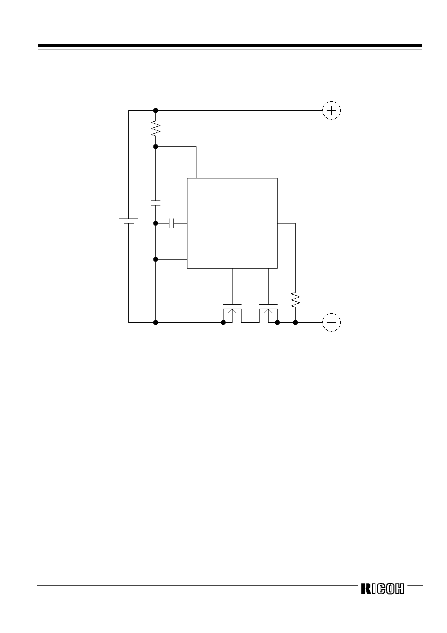
- 9 -
n
TYPICAL APPLICATION
5
2
3
1
6
0.1
m
F
4
0.01
m
F
1k
W
330
W
R5422N
n
APPLICATION HINTS
R1 and C1 will stabilize a supply voltage to the R5422Nxxxx. A recommended R1 value is less than 1k
W.
A larger value of R1 leads higher detection voltage, makes some errors, because of shoot through current flowed in the
R5422Nxxxx.
R2 will stabilize a V- pin voltage. The resetting from over-discharge with connecting a charger possibly be disabled by larger
value of R2. Recommended value is less than 1 k
W.
R1 and R2 can operate also as a part of current limit circuit against for setting cell reverse direction or for applying excess
charging voltage to the R5422Nxxxx, battery pack, while smaller R1 and R2 may cause a power consumption over rating of
power dissipation of the R5422Nxxxx and a total of 'R1+R2' should be more than 1k
W.