 | –≠–ª–µ–∫—Ç—Ä–æ–Ω–Ω—ã–π –∫–æ–º–ø–æ–Ω–µ–Ω—Ç: R5534V | –°–∫–∞—á–∞—Ç—å:  PDF PDF  ZIP ZIP |
R5534V
May. 2005
Rev. 1.10
- 1 -
PCMCIA Power Controller
s
s
s
s
DESCRIPTION
The R5534V switches between the three V
CC
voltages (0V/3.3V/5.0V) and the V
PP
voltages (off/0V/3.3V/5.0V).
The R5534V has two sets of V
CC
output and V
PP
output each, therefore it fits dual slot models. If V
CC
pin or V
PP
pin
may be clamped to the GND, short current limit works at 1A(Min.) for VCC and 0.15A(Min.) for V
PP
.
The R5534V is suitable for standard PCMCIA power controllers.
s
s
s
s
FEATURES
z Low on resistance P-channel MOSFET Switch
z Dual Slot Power Supply Control
z Over- Current Limit Protection
z Thermal Shutdown Protection
z Low Consumption Current
z Break-Before-Make Switching
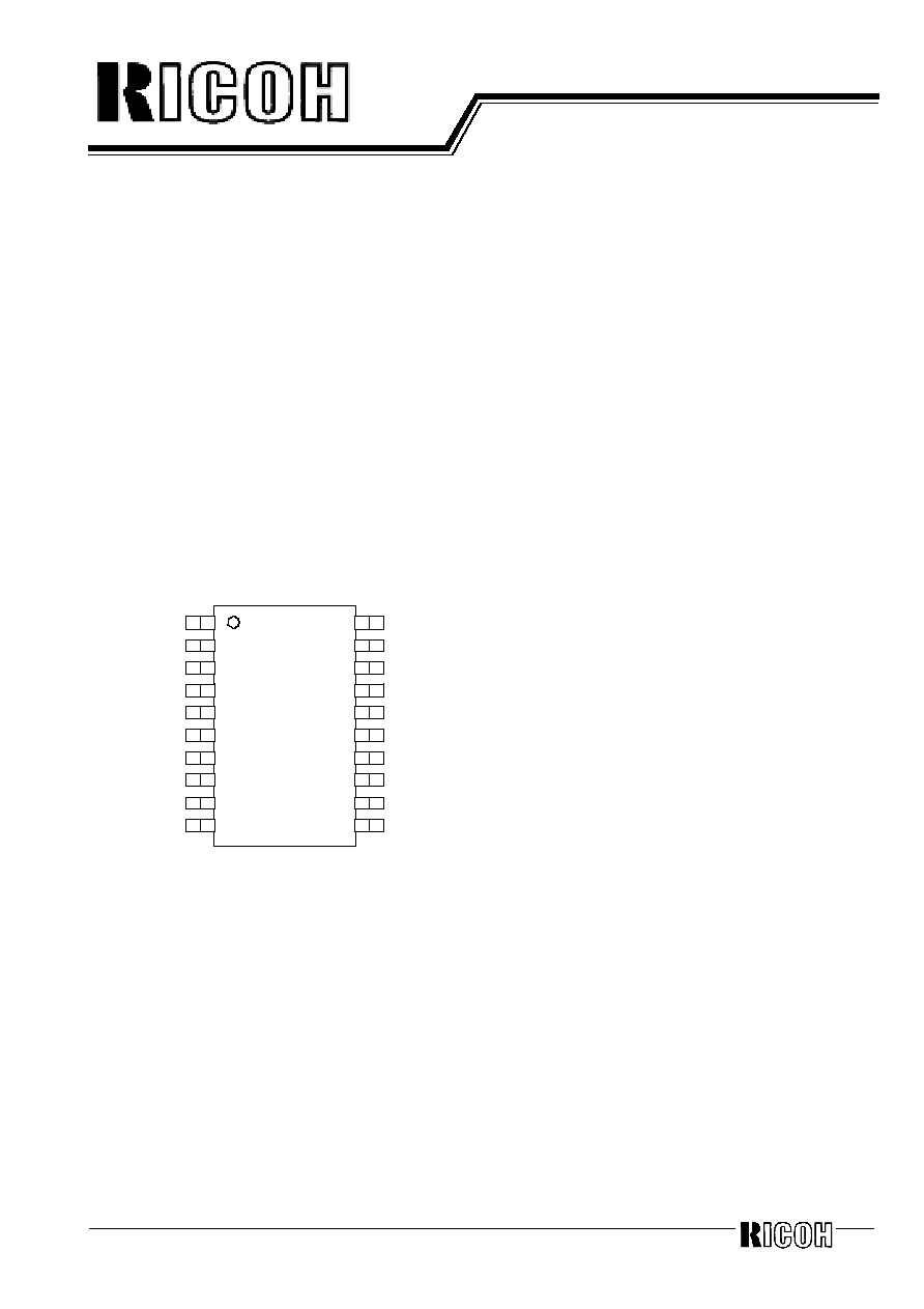
z SSOP-20 pin Package
s
s
s
s
APPLICATIONS
Dual Slot PC card Power Supply Pin Voltage Switch
Card-bus Slot Power Supply Control
PC Card Reader/Writer
s
PIN CONFIGURATION
1
2
3
4
5
6
7
8
20
19
18
17
9
10
11
12
16
15
14
13
V
CC3
IN
AV
CC
OUT
BEN0
AV
CC
OUT
AV
PP
OUT
BEN1
BV
CC5_EN
BV
CC3_EN
V
CC5
IN
GND
AEN1
AV
CC5_EN
AEN0
BV
CC
OUT
BV
PP
OUT
BV
CC
OUT
TST
AV
CC3_EN
V
CC3
IN
V
CC5
IN
*Note: Same name pins should be connected one another.
Connect TST pin to V
CC
5IN pin.

Rev. 1.10
- 2 -
s
s
s
s
BLOCK DIAGRAM
THERMAL
SHUTDOWN
GATE
CONTROL
LOGIC
CURRENT
LIMIT
V
CC5
IN
B V
PP
OUT
B V
CC
OUT
V
CC3
IN
B EN1
B EN0
B V
CC5_EN
B V
CC3_EN
GND
GATE
CONTROL
LOGIC
CURRENT
LIMIT
V
CC5
IN
AV
PP
OUT
AV
CC
OUT
V
CC3
IN
A EN1
A EN0
AV
CC5_EN
AV
CC3_EN
s
PIN DESCRIPTION
Symbol Pin description
V
CC5IN
5V Input Pin
V
CC3IN
3V Input Pin
GND
Ground Pin
V
CC5_EN
Logic Input Pin
V
CC3_EN
Logic Input Pin
EN1
Logic Input Pin
EN0
Logic Input Pin
V
CCOUT
V
CC
Output Pin
V
PPOUT
V
PP
Output Pin
TST
Test Pin

12345
Rev. 1.10
- 3 -
s
ABSOLUTE MAXIMUM RATINGS
Topt=25
∞
C
Item Symbol
Conditions
Ratings Unit
Input Voltage (5V)
V
cc5IN
-0.3 to 6.0
V
Input Voltage (3V)
V
cc3IN
-0.3 to 6.0
V
Logic Input Voltage
V
IN
-0.3 to 6.0
V
TST Input Voltage
V
TST
-0.3 to 6.0
V
I
O (VCC)
Each Slot
>1A, Internal Limited
Output Current
I
O (VPP)
Each Slot
>150mA, Internal Limited
Power Dissipation
P
D
Internal Limited
Operating Temperature Range
Topt
-40 to 85
∞
C
Storage Temperature Range
Tstg
-55 to 125
∞
C
*Note: Absolute maximum ratings are threshold limit values that must not be exceeded even for any
moment under any conditions. More over, such values for any two or more items of the ratings must not
be reached simultaneously. Operation above these absolute maximum ratings may cause degradation or
fatal damage to the device. These mean stress ratings and do not necessarily imply functional operation
below these limits.
Rev. 1.10
- 4 -
s
ELECTRICAL CHARACTERISTICS
Topt=25
∞
C
Symbol Item
Conditions
Min.
Typ.
Max.
Unit
V
cc5
Supply
Voltage
(5V)
3.0 5.0 5.5 V
V
cc3
Supply
Voltage
(3V)
3.0 3.3 5.5 V
I
cc5
Vcc
OUT
= 5V or 3.3V
60
120
µ
A
I
SLP5
Vcc
OUT
= 0V (sleep mode)
0.2
10.0
µ
A
I
CC3
Vcc
OUT
= 5V or 3.3V
20
60
µ
A
I
SLP3
Supply Current
Vcc
OUT
= 0V (sleep mode)
0.1
10
µ
A
Select Vcc
OUT
=5V, Vcc5IN=5.0V
110
170
m
Select Vcc
OUT
=3.3V, Vcc3IN=3.3V
130
180
m
RoV
cc
Vcc
OUT
switch resistance
Select Vcc
OUT
=0V, Vcc5IN=5.0V
500
3900
Select Vpp
OUT
=5V, Vcc5IN=5.0V
2.1
3.5
Select Vpp
OUT
=3.3V,
Vcc3IN=3.3V
3.3 5.5
RoV
pp
Vpp
OUT
switch resistance
Select Vpp
OUT
=0V, Vcc5IN=5.0V
2500
3900
I
PPL
Vpp
OUT
Leakage Current
Select Vpp
OUT
=Hi-Z
1
10
µ
A
I
CCSC
Vcc
OUT
=0V 1
1.5
A
I
PPSC
Short Current Limit
V
PP OUT
=0V 0.15
0.40
A
V
IH
Logic Input "H" Voltage
2.2
6.0
V
V
IL
Logic Input "L" Voltage
-0.3
0.8
V
I
IN
Logic
Input
Current
-1
1
µ
A
T
SD
Thermal Shutdown Temperature
135
∞
C
t1 Vcc
OUT
=0V to 10% of 3.3V
(Select 3.3V)
200
µ
s
t
2
Vcc Turn-on Delay Time
(*Note 2)
Vcc
OUT
=0V to 10% of 5.0V(Select 5V)
400
µ
s
t
3
Vcc
OUT
=10% to 90% of 3.3V
(Select 3.3V)
800
µ
s
t
4
Vcc Rising Time (*Note 2)
Vcc
OUT
=10% to 90% of 5.0V(Select 5V)
2300
µ
s
t
7
Vcc
OUT
=3.3V to Hi-Z
2.3
ms
t
8
Vcc Turn-off Delay Time
(*Note1,2,4)
Vcc
OUT
=5V to Hi-Z
2.8
ms
t5 Vcc
OUT
=90% to 10% of 3.3V
(Select 3.3V)
800
µ
s
t6
V
cc
Falling Time (*Note 3)
Vcc
OUT
=90% to 10% of 5.0V(Select 5V)
700
µ
s
t9 Vpp
OUT
=0V to 10% of 3.3V
(Select 3.3V)
5
µ
s
t10
Vpp Turn-on Delay Time
(*Note 3)
Vpp
OUT
=0V to 10% of 5.0V(Select 5V)
12
µ
s
t11 Vpp
OUT
=10% to 90% of 3.3V
(Select 3.3V)
300
µ
s
t12
Vpp Rising Time (*Note 3)
Vpp
OUT
=10% to 90% of 5.0V(Select 5V)
360
µ
s
t15 Vpp
OUT
=3.3V to Hi-Z
0.1
µ
s
t16
Vpp Turn-off Delay Time
(*Note 1,3)
Vpp
OUT
=5V to Hi-Z
0.1
µ
s
t13 Vpp
OUT
=90% to 10% of 3.3V
(Select 3.3V)
0.05
µ
s
t14
Vpp Falling Time (*Note 3)
Vpp
OUT
=90% to 10% of 5.0V(Select 5V)
0.05
µ
s
(*Note1) Delay from commanding Hi-Z or 0V to beginning slope
(*Note2) t1 to t8 Test Condition: RL=10
(*Note3) t9 to t15 Test Condition: RL=100
(*Note4) Do not apply to current limit or thermal shutdown conditions during these terms

12345
Rev. 1.10
- 5 -
Fig.1 R5534V Vcc Timing Diagram
V
CC
Enable
V
CC
Output
Vcc to 5V
FLG
0 V
Vcc to 3.3V
C
D
B
A
0 V
0 V
t7
t8
t3
t 1
t5
t4
t 2
t6
Vcc OFF
Vcc OFF
Fig. 2 R5534V V
PP
Timing Diagram
V
PP
Enable
V
PP
Output
V
PP
to 5V
V
PP
to 3.3V
C
D
B
A
0 V
0 V
t15
t16
t11
t 9
t13
t12
t 10
t14
V
PP
OFF
V
PP
OFF

Rev. 1.10
- 6 -
R5534V Control Logic Table
Vcc
5_EN
Vcc
3_EN
EN1 EN0 Vcc
OUT
Vpp
OUT
0 0 0 0 0V
0V
0 0 0 1 0V
Hi-Z
0 0 1 0 0V
Hi-Z
0 0 1 1 0V
Hi-Z
0 1 0 0 5V
0V
0 1 0 1 5V
5V
0 1 1 0 5V
Hi-Z
0 1 1 1 5V
Hi-Z
1 0 0 0 3.3V
0V
1 0 0 1 3.3V
3.3V
1 0 1 0 3.3V
Hi-Z
1 0 1 1 3.3V
Hi-Z
1 1 0 0 0V
0V
1 1 0 1 0V
Hi-Z
1 1 1 0 0V
Hi-Z
1 1 1 1 0V
Hi-Z
s
OPERATION
When the Vcc
OUT
=0V is selected, the IC switches into the sleep mode, and draws only some nano-amperes of leakage current.
Without being V
CCOUT
=0V, if commanded to immediately switch from 5V to 3.3V or vice versa, enhancement of the second
switch begins after the first is OFF, realizing break-before-make protection.
In case that an OUT pin may be clamped to the GND, if over-current would continue, the temperature of the IC would increase
drastically. If the temperature of the IC is beyond 135
∞
C, the switch transistor turns off. Then, when the temperature of the IC
decreases equal or lower than 125
∞
C, the switch transistor turns on. Unless the abnormal situation of OUT pin is removed or
turned off, the switch transistor repeats on and off.
Short over-current level is set internally in the IC. There are two types of response against over-current: Under the condition
that OUT pin is short or large capacity is loaded, if the IC is enabled, the IC becomes constant current state immediately.
Current level of constant current is short current limit. While the switch transistor is on, if OUT pin is short or large capacity is
loaded, until the current limit circuit responds, large transient current flows. The transient current depends on the impedance
between the power supply circuit, V
CC5IN
/V
CC3IN
and load capacitance. In other words, the transient current depends on the
transient response characteristics of the power supply circuit, V
CC5IN
/V
CC3IN
, PCB layout, and the connector of the card. After
the transient current is beyond the current limit threshold and current limit circuit responds, the IC becomes into the constant
current mode, and the current level is equal to short current limit.
s
s
s
s
APPLICATION NOTES
* V
CC5IN
voltage should be equal or more than V
CC3IN
.
* Same name pins should be connected one another.
* There is a parasitic diode between source and drain of the switch transistors. (Refer to the block diagram.)
Therefore, even If the switch may be disabled, in case the OUT voltage is higher than V
CC5IN
, some current flows
from OUT to V
CC5IN
.
* Connect TST pin to Vcc
5IN
* Set a bypass capacitor with capacitance ranging from 0.1
µ
F to 1.0
µ
F between V
CC5IN
pin and GND pin, and
between V
CC3IN
and GND pin each.

12345
Rev. 1.10
- 7 -
s
TYPICAL CHARACTERISTICS
1)V
CCOUT
Switch Resistance vs. Temperature
(Select VCCOUT=5V)
2)V
CCOUT
Switch Resistance vs. Temperature
(Select VCCOUT=3.3V)
40
60
80
100
120
140
160
180
-50
-25
0
25
50
75
100
Temperature Topt
Vcco
u
t
sw
i
t
ch
r
e
si
sta
n
c
e
R
o
Vc
c
[
m
ohm
]
(
5V
S
W
)
VCC5IN=5V
VCC3IN=3.3V
IOUT=1A
40
60
80
100
120
140
160
180
-50
-25
0
25
50
75
100
Temperature Topt
Vcco
u
t
sw
i
t
ch
r
e
si
sta
n
c
e
R
o
Vc
c
[
m
ohm
]
(
3.
3V
S
W
)
VCC5IN=5V
VCC3IN=3.3V
IOUT=1A
3) Vcc Turn-on Delay Time, Vcc Rising Time
(Select VCCOUT=5V)
4)Vcc Turn-off Delay Time, Vcc Falling Time
(Select VCCOUT=5V)
EN0=0V
EN1=0V
VCC3_EN=5V
R
L
=10
VCC5_EN
VCCOUT
EN0=0V
EN1=0V
VCC3_EN=5V
R
L
=10
VCC5_EN
VCCOUT
5) Vcc Turn-on Delay Time, Vcc Rising Time
(Select VCCOUT=3.3V)
6)Vcc Turn-off Delay Time, Vcc Falling Time
(Select VCCOUT=3.3V)
EN0=0V
EN1=0V
VCC5_EN=5V
R
L
=10
VCC3_EN
VCCOUT
EN0=0V
EN1=0V
VCC5_EN=5V
R
L
=10
VCC3_EN
VCCOUT
(
∞
C)
(
∞
C)