 | –≠–ª–µ–∫—Ç—Ä–æ–Ω–Ω—ã–π –∫–æ–º–ø–æ–Ω–µ–Ω—Ç: RF5C15 | –°–∫–∞—á–∞—Ç—å:  PDF PDF  ZIP ZIP |
DISCONTINUED
REAL-TIME CLOCK
1
RP/RF/RJ5C15
OUTLINE
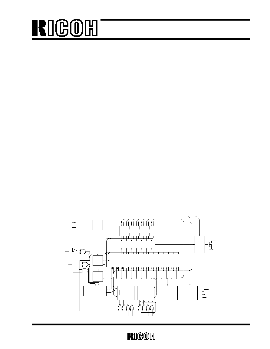
The RP/RF/RJ5C15 are real-time clocks for microcomputers that can be connected directly to data buses of
16bit CPUs, such as the 8086, Z8000, and 68000, and of 8bit CPUs, such as the 8085A, Z80, 6809, and 6502. They
allow setting or reading of the clock with the same procedures as for the Read/Write operation for memory.
These products have various features including clock, calendar and alarm functions and can be backed up by
batteries.
∑ Connected directly to CPU enabling fast access. ∑ 4bit bidirectional data bus : D0 - D3
∑ 4bit address input : A0 - A3
∑ Built-in clock counter (hour, minute, second) and calendar counter (leap year, year, month, day, day-of-the-week)
∑ All clock data expressed in BCD codes
∑ Backed up by batteries (minimum : 2.0V)
∑ Selectable basic clock frequency : 16kHz, 1kHz, 128Hz, 16Hz, 1Hz, 1/60Hz.
∑ Outputs alarm signals or timing pulse of 16Hz or 1Hz. ∑ CMOS technology
∑ Supply voltage : Single power supply of +5V
∑ Packages RP5C15......18pin DIP
RF5C15......18pin SOP
RJ5C15......28pin PLCC
FEATURES
NO. EK-086-9908
BLOCK DIAGRAM
S1 S2 S3 S4 S5 S6 S7 S8 S9 SA SB SC
OSCIN
OSCOUT
CS
CS
RD
WR
OSC
1/2
15
16
k
H
z
, 1
k
H
z
, 128H
z
, 16H
z
, 1H
z
, 1/60H
z
1H
z
, 16H
z
T.RESET
RD.WR.
BANK 1
ALARM
RESET
RD. WR.
ALARM
ALARM
OUTPUT
BANK 0. RD. WR.
CLOCK
HOLD
ADJ
HOLD
CONTROLLER
SO
SF
ADDRESS
DECODER
BUS
CONTROL
CLOCK
SELECT
CLOCK
OUTPUT
CLKOUT
ALARM
3
SD
-SF
4
4
3 4
3
4
2
3
4
2
4
1
4
4
2
S0
SECONDS MINUTES
HOURS
DAYS
MONTHS
YEARS
WEEK
LEAP YEARS
COMPARATOR
ALARM REGISTER
4
3
4
2
3
4
2
S
2
S
3
S
4
S
5
S
6
S
7
S
8
A
0
A
1
A
2
A
3
D
0
D
1
D
2
D
3
1
/
10
1
/
6
1
/
10
1
/
6
1
/
12
1
/
24
1
/
7
1
/
10
1
/
10
1
/
4
1
/
28
-
1
/
31
1
/
12
RP/RF/RJ5C15
2
DISCONTINUED
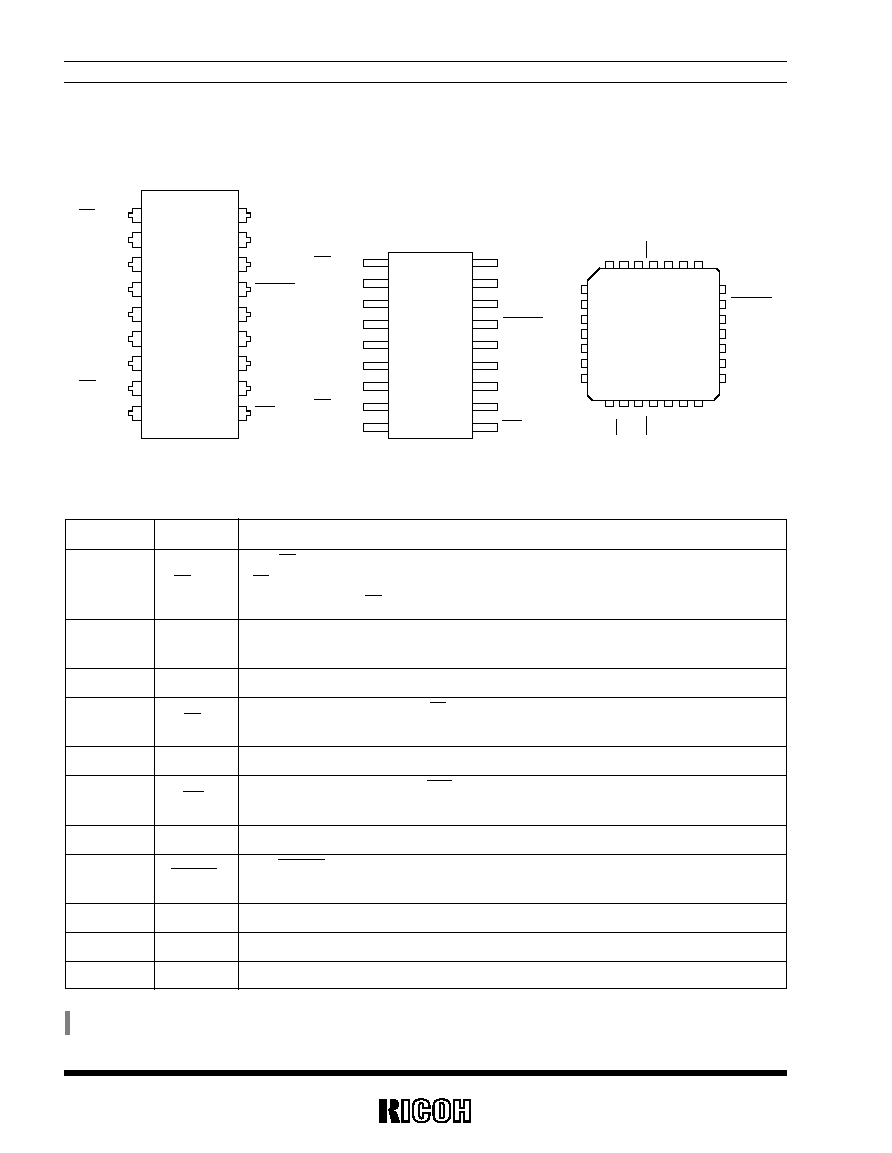
PIN CONFIGURATIONS
CS
CS
CLKOUT
A
0
A
1
A
2
A
3
RD
GND
V
CC
OSCOUT
OSCIN
ALARM
D
3
D
2
D
1
D
0
WR
CS
CS
CLKOUT
A
0
A
1
A
2
A
3
RD
GND
V
CC
OSCOUT
OSCIN
ALARM
D
3
D
2
D
1
D
0
WR
NC
A
0
NC
A
1
NC
A
2
NC
N
C
C
L
K
O
U
T
C
S
C
S
V
c
c
O
S
C
O
U
T
O
S
C
I
N
NC
ALARM
NC
D
3
NC
D
2
NC
5
6
7
8
9
10
11
25
24
23
22
21
20
19
12 13 14 15 16 17 18
4 3 2 1 28 27 26
A
3
R
D
G
N
D
W
R
N
C
D
0
D
1
1
2
3
4
5
6
7
8
9
18
17
16
15
14
13
12
11
10
1
2
3
4
5
6
7
8
9
18
17
16
15
14
13
12
11
10
∑
RP5C15 (18pin DIP)
∑
RF5C15 (18pin SOP)
∑
RJ5C15 (28pin PLCC)
PIN DESCRIPTION
*
) Pin numbers shown are for the RP5C15 and the RF5C15. These are different for the RJ5C15.
For specific pin number see the "PIN CONFIGURATIONS".
Pin No.
Symbol
Function
1,2
CS, CS
The CS and CS are used to interface with external devices. Enabled when CS ="H" and
CS="L". The CS is connected to the power down detector in the system power supply
assembly while the CS is connected to the microcomputer.
3
CLKOUT
Output pin for reference clock pulse and an open drain output. Selectable from 8 modes
based on the setting of the clock select register as shown in the separate table.
4,5,6,7
A
0
to A
3
Input pins for the address signal. These pins are connected to the CPU address bus.
8
RD
Input pin for I/O control. The RD is set to "L" when data is transferred from the
RP/RF/RJ5C15 to the CPU.
9
GND
Ground pin for the power supply of 0V.
10
WR
Input pin for I/O control. The WR is set to "L" when data is transferred from the CPU to
the RP/RF/RJ5C15.
11,12,13,14
D
0
to D
3
Bidirectional data bus. Connected to the data bus of the CPU.
15
ALARM
The ALARM outputs alarm signal and 16Hz and 1Hz clock pulses. This pin is an open
drain output.
16
OSCIN
The OSCIN and OSCOUT are connected to the 32.768kHz crystal oscillator.
17
OSCOUT
32.768kHz
18
V
CC
Input pin for the power supply of +5V.
DISCONTINUED
Absolute Maximum ratings are threshold limit values that must not be exceeded even for an instant under
any conditions. Moreover, such values for any two items must not be reached simultaneously. Operation
above these absolute maximum ratings may cause degradation or permanent damage to the device. These
are stress ratings only and do not necessarily imply functional operation below these limits.
RP/RF/RJ5C15
3
ABSOLUTE MAXIMUM RATINGS
RECOMMENDED OPERATING CONDITIONS
Symbol
Item
Conditions
Ratings
Unit
V
CC
Supply Voltage
≠0.3 to 7.0
V
V
I
Input Voltage
≠0.3 to V
CC
+0.3
V
V
O
Output Voltage
≠0.3 to V
CC
+0.3
V
Pd
Maximum Power Dissipation
Ta=25∞C
400
mW
Topr
Operating Temperature
≠20 to 70
∞C
Tstg
Storage Temperature
≠40 to 125
∞C
Symbol
Item
Conditions
MIN.
TYP.
MAX.
Unit
V
CC
Supply Voltage
4.5
5
5.5
V
V
DH
Data Preservation Voltage
2.0
5.5
V
f
XT
Crystal Oscillation Frequency
32.768
kHz
Referenced at GND pin
(Unless otherwise specified, Ta=≠20 to 70∞C)
ABSOLUTE MAXIMUM RATINGS
RP/RF/RJ5C15
4
DISCONTINUED
DC ELECTRICAL CHARACTERISTICS
Symbol
Item
Conditions
MIN.
TYP.
MAX.
Unit
V
IH
"H" Input Voltage (excluding OSCIN)
2.0
Vcc+0.3
V
"H" Input Voltage (OSCIN)
2.4
Vcc+0.3
V
V
IL
"L" Input Voltage (excluding OSCIN)
≠0.3
0.8
V
"L" Input Voltage (OSCIN)
≠0.3
0.5
V
V
OH
"H" Output Voltage
I
OH
=≠400µA
2.4
V
V
OL
"L" Output Voltage
I
OL
=2mA
0.4
V
I
LI
Input Leakage Current
V
IN
=0 to Vcc
≠10
10
µA
I
OZ
Output Off-state Leakage Current
Voz=0 to 5.5V
±10
µA
I
CC1
Supply Current for Backup
f
XT
=32.768kHz, Vcc=2.0V
15
µA
I
CC2
Operating Supply Current
f
XT
=32.768kHz, Vcc=5.5V*
250
µA
V
ILCS
CS pin "L" Input Voltage for Backup
Vcc=2.0V
≠0.2
0.2
V
V
IHCS
CS pin "H" Input Voltage for Backup
Vcc=2.0V
1.8
2.0
V
(Unless otherwise specified, Ta=≠20 to 70∞C, Vcc=5V±10%)
*
) RD, WR signal frequency : 100kHz ; Input pin is fixed at Vcc or GND level ; output pin open.
AC ELECTRICAL CHARACTERISTICS
Symbol
Item
Conditions
MIN.
TYP.
MAX.
Unit
t
AC
Address≠RD/WR Delay Time
50
ns
t
cc
RD/WR Pulse Width
120
13000
ns
t
CA
Address Effective Time after rising
10
ns
of RD/WR
t
RD
Data Delay Time after falling of RD
1TTL+100pF
120
ns
t
RDH
Data Hold Time after rising of RD
10
ns
t
WDS
Data Setup Time in Write operation
100
ns
t
WDH
Data Hold Time in Write operation
20
ns
t
TED
Timer Enable to Timer Disable
100
µs
t
ADJ
Adjust Completion Time
100
µs
t
AINH
Alarm Write Inhibit Time after Resetting
100
µs
t
RCV
RD/WR Recovery Time
1
µs
(Unless otherwise specified, Ta=≠20 to 70∞C, Vcc=5V±10%)
RP/RF/RJ5C15
5
DISCONTINUED
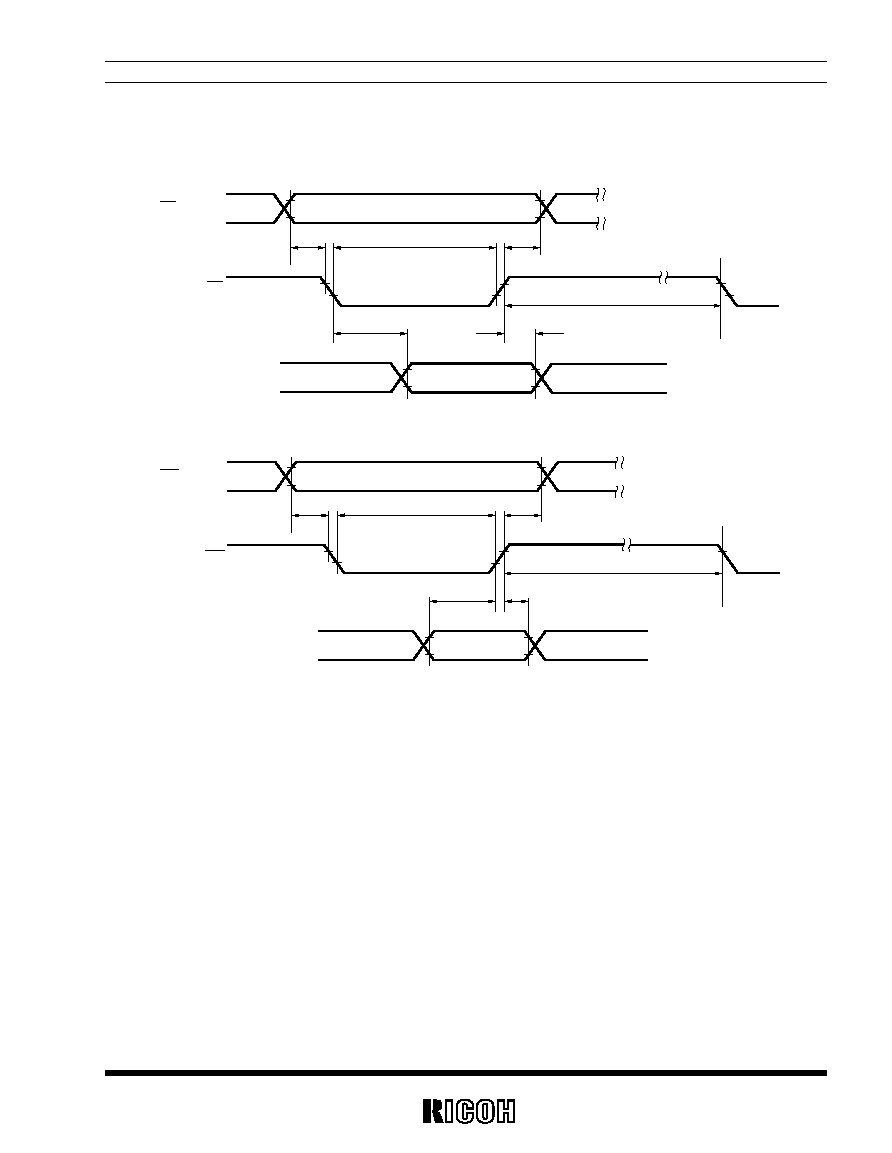
TIMING CHART
Valid
CS, A
0
to A
3
RD
D
0
to D
3
Valid
t
AC
t
CC
t
RD
t
RCV
t
RDH
t
CA
∑
Read Cycle
t
WDH
Valid
CS, A
0
to A
3
WR
D
0
to D
3
Valid
t
AC
t
CC
t
RCV
t
CA
t
WDS
∑
Write Cycle
RP/RF/RJ5C15
6
DISCONTINUED
MODE
BANK 0
BANK 1
A3 to A0
Description
D3
D2
D1
D0
Description
D3
D2
D1
D0
0
1-second counter
Clock output select
◊
register
1
10-second counter
◊
Adjust
◊
◊
◊
ADJ
2
1-minute counter
1-minute alarm register
3
10-minute counter
◊
10-minute alarm register
◊
4
1-hour counter
1-hour alarm register
5
10-hour counter
◊
◊
10-hour alarm register
◊
◊
6
Day-of-the-week counter
◊
Day-of-the-week alarm register
◊
7
1-day counter
1-day alarm register
8
10-day counter
◊
◊
10-day alarm register
◊
◊
9
1-month counter
◊
◊
◊
◊
A
10-month counter
◊
◊
◊
12/24 select register
◊
◊
◊
B
1-year counter
Leap year counter
◊
◊
C
10-year counter
◊
◊
◊
◊
D
MODE register
Timer EN Alarm EN
◊
BANK1/0
Timer EN Alarm EN
◊
BANK1/0
E
TEST register
Test 3
Test 2
Test 1
Test 0
Test 3
Test 2
Test 1
Test 0
F
RESET controller, etc. 1Hz ON 16Hz ON
Timer RESET Alarm RESET
1Hz ON 16Hz ON
Timer RESET Alarm RESET
*
) "x" means "Don't care" for Write ; always "0" for Read.
ADDRESS MAPPING
∑
Clock Output Select Register (BANK 1, Address 0h)
D3
D2
D1
D0
Clock Output
Remarks
◊
0
0
0
"Z"
High impedance
◊
0
0
1
16.384kHz
duty 50%
◊
0
1
0
1.024kHz
duty 50%
◊
0
1
1
128Hz
duty 50%
◊
1
0
0
16Hz
duty 50%
◊
1
0
1
1Hz
duty 50% When the second counter counts up.
◊
1
1
0
1/60Hz
duty 50% When the second counter counts up.
◊
1
1
1
"L"
*
) "x" means "Don't care" for Write ; always "0" for Read.

RP/RF/RJ5C15
7
DISCONTINUED
∑ ADJ (BANK1, Address 1h, D
0
)
Bit for correcting the second digit. When set to 1,
1) For digits ranging from 00 to 29 : Resets the lower-order counter than the 1-second counter and sets the second
digit to 00.
2) For digits ranging from 30 to 59 : Resets the lower-order counter than the 1-second counter, sets the second
digit to 00 and increments the minute digit by 1.
∑ MODE register (BANK1/0, Address Dh)
*
) When the Timer EN is set to 0, the 1-second counter and higher-order counters than the 1-second counter stop. If any carrying occurs in the lower-
order counters than the 1-second counter while the Timer EN is 0, carrying will be held and avoided until the Timer EN changes from 0 to 1. Thus, no
apparent delay is produced when the duration of the Timer EN = 0 is less than one second.
1: BANK1 : Setting and reading of alarm, 12-hour/24-hour,
leap year, clock output selection and adjust operation.
0: BANK0 : Setting and reading of time
1: Alarm output enable
0: Alarm output disable
(Note that 16Hz or 1Hz signals are not affected.)
1: Counting time starts ; 0 : the 1-second counter and
higher-order counters than the 1-second counter stop*
D
3
D
2
D
1
D
0
Timer EN Alarm EN
◊
BANK1/0
∑ 12/24 select register (BANK1, Address Ah)
D
0
=1 sets to 24-hour system ; D
0
=0 sets to 12-hour system.
Set the 10-hour counter as D
1
=1 for p.m., D
1
=0 for a.m.
∑ Leap year counter (BANK1, Address Bh)
(D
1
, D
0
)=(0, 0) sets the counter for leap years. The counter value changes in the order of (0, 0) (0, 1) (1, 0) (1, 1)
(0, 0) repeatedly in the same timing as the year counter.
∑ RESET controller/16Hz ∑ 1Hz clock register. (BANK1/0, Address Fh)
D
0
=1 : Resets all alarm registers.
D
1
=1 : Resets divider stages for seconds or smaller units.
D
2
=0 : 16Hz clock pulse ON.
D
3
=0 : 1Hz clock pulse ON.
∑ Test register (BANK1/0, Address Eh)
Register used for LSI inspection. Recommended setting is (D
3
, D
2
, D
1
, D
0
)=(0, 0, 0, 0)
*
) Addresses 0h to Dh are applicable both for Read and Write.
*
) Addresses Eh to Fh are applicable only for Write.
RP/RF/RJ5C15
8
DISCONTINUED
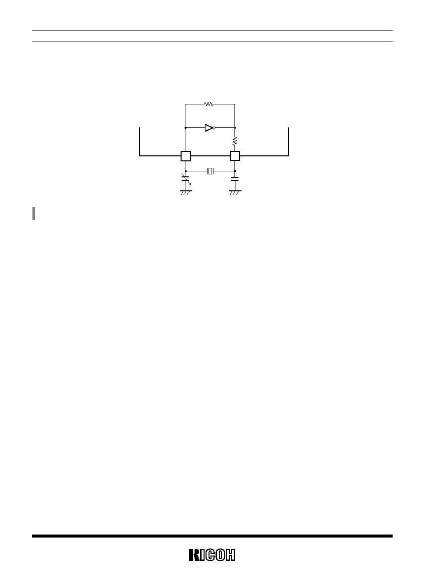
OSCILLATOR CIRCUIT
Since this circuit includes an output ballast resistor (=70k), no external device is necessary.
RP/RF/RJ5C15
OSCIN
OSCOUT
C
I
Co
32.768
k
H
z
70k
16
17
C
I
=Variable between 10 and 30pF.
C
O
=Standard 30pF
*
) Values of C
I
and C
O
are for reference only.
*
) In the RJ5C15, the OSCIN is 26pin and the OSCOUT is 27pin.
. .
DISCONTINUED
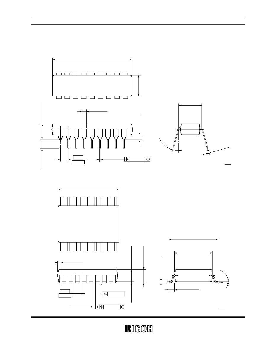
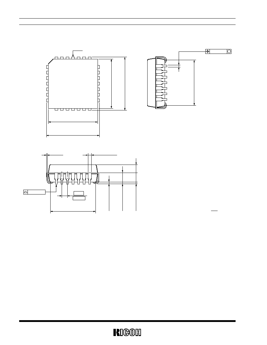
PACKAGE DIMENSIONS
∑ RP5C15 (18pin DIP)
24.8max.
0.976max.
6
.
4
±
0
.
2
0
.
2
5
2
±
0
.
0
0
8
18
1
10
9
1.5typ.
0.059typ.
4
.
7
m
a
x
.
0
.
1
8
5
m
a
x
.
0
.
5
1
m
i
n
.
0
.
0
2
0
m
i
n
.
2
.
8
m
i
n
.
0
.
1
1
0
m
i
n
.
2.54
0.100
0.46 +0.15
≠0.1
0.018+0.006
≠0.004
M
0.25(0.010)
0.25
+0.1
5
≠0.0
5
0.01
0
+0.0
06
≠0.0
02
7.62
0.300
0
∞
to
15
∞
(Unit : )
mm
inch
∑ RF5C15 (18pin SOP)
0.775max.
0.031max.
0.41
±
0.1
0.016
±
0.004
11.71max.
0.461max.
18
1
10
9
1.27
0.050
M
0.12(0.005)
0.12(0.005)
2
.
3
4
±
0
.
1
0
.
0
9
2
±
0
.
0
0
4
0
.
2
2
t
y
p
.
0
.
0
0
9
t
y
p
.
2
.
6
4
m
a
x
.
0
.
1
0
4
m
a
x
.
7.52
±
0.2
0.296
±
0.008
0.81
±
0.2
0.032
±
0.008
10.31
±
0.3
0.406
±
0.012
0
.
2
5
+
0
.
1
≠
0
.
0
5
0
.
0
1
0
+
0
.
0
0
4
≠
0
.
0
0
2
0∞
to
1
0
∞
(Unit : )
mm
inch
RP/RF/RJ5C15
9
RP/RF/RJ5C15
10
DISCONTINUED
∑ RJ5C15 (24pin PLCC)
11.48typ.
0.452typ.
0.490
±
0.005
12.45+0.12
≠0.13
1
1
.
4
8
t
y
p
.
0
.
4
5
2
t
y
p
.
0
.
4
9
0
±
0
.
0
0
5
1
2
.
4
5
+
0
.
1
2
≠
0
.
1
3
1
0
.
6
7
+
0
.
2
5
≠
0
.
7
6
0
.
4
2
0
+
0
.
0
1
≠
0
.
0
3
0.432
±
0.10
0.017
±
0.004
M
0.18(0.007)
0.254
0.010
0.737
±
0.076
0.029
±
0.003
10.67 +0.25
≠0.76
0.420 +0.01
≠0.03
1.27
0.050
0.10(0.004)
4
.
5
7
m
a
x
.
0
.
1
8
0
m
a
x
.
2
.
5
6
+
0
.
2
3
≠
0
.
0
2
0
.
1
0
1
+
0
.
0
0
9
≠
0
.
0
0
1
0
.
5
0
8
m
i
n
.
0
.
0
2
0
m
i
n
.
Pin No.1
(Unit : )
mm
inch

NOTICE
1. The products and the product specifications described in this document are subject to change or discontinuation
of production without notice for reasons such as improvement. Therefore, before deciding to use the products,
please refer to Ricoh sales representatives for the latest information thereon.
2. This document may not be copied or otherwise reproduced in whole or in part without prior written consent of
Ricoh.
3. Please be sure to take any necessary formalities under relevant laws or regulations before exporting or other-
wise taking out of your country the products or the technical information described herein.
4. The technical information described in this document shows typical characteristics of and example application
circuits for the products. The release of such information is not to be construed as a warranty of or a grant of
license under Ricoh's or any third party's intellectual property rights or any other rights.
5. The products listed in this document are intended and designed for use as general electronic components in
standard applications (office equipment, computer equipment, measuring instruments, consumer electronic
products, amusement equipment etc.). Those customers intending to use a product in an application requiring
extreme quality and reliability, for example, in a highly specific application where the failure or misoperation of
the product could result in human injury or death (aircraft, spacevehicle, nuclear reactor control system, traffic
control system, automotive and transportation equipment, combustion equipment, safety devices, life support
system etc.) should first contact us.
6. We are making our continuous effort to improve the quality and reliability of our products, but semiconductor
products are likely to fail with certain probability. In order prevent any injury to persons or damages to property
resulting from such failure, customers should be careful enough to incorporate safety measures in their design,
such as redundancy feature, fire-containment feature and fail-safe feature. We do not assume any liability or
responsibility for any loss or damage arising from misuse or inappropriate use of the products.
7. Anti-radiation design is not implemented in the products described in this document.
8. Please contact Ricoh sales representatives should you have any questions or comments concerning the prod-
ucts or the technical information.
June 1995

RICOH COMPANY, LTD.
ELECTRONIC DEVICES DIVISION
HEADQUARTERS
13-1, Himemuro-cho, Ikeda City, Osaka 563-8501, JAPAN
Phone +81-727-53-6003 Fax +81-727-53-2120
YOKOHAMA OFFICE (International Sales)
3-2-3, Shin-Yokohama, Kohoku-ku, Yokohama City, Kanagawa 222-8530,
JAPAN
Phone +81-45-477-1697 Fax +81-45-477-1694 ∑ 1695
http://www.ricoh.co.jp/LSI/english/
RICOH CORPORATION
ELECTRONIC DEVICES DIVISION
SAN JOSE OFFICE
1996 Lundy Avenue, San Jose, CA 95131, U.S.A.
Phone +1-408-944-3306 Fax +1-408-432-8375
http://www.ricoh-usa.com/semicond.htm