 | –≠–ª–µ–∫—Ç—Ä–æ–Ω–Ω—ã–π –∫–æ–º–ø–æ–Ω–µ–Ω—Ç: RH5RE58A | –°–∫–∞—á–∞—Ç—å:  PDF PDF  ZIP ZIP |
VOLTAGE REGULATOR
FOR MIDDLE OUTPUT CURRENT
1
Rx5RE SERIES
OUTLINE
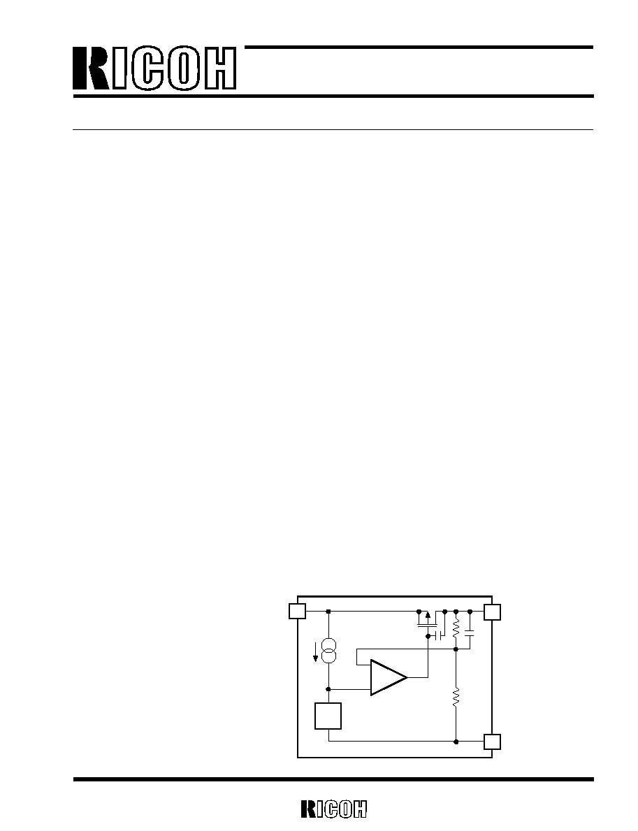
The Rx5RE Series are CMOS-based voltage regulator ICs with high output voltage accuracy and ultra-
low quiescent current. Each of these ICs consists of a voltage reference unit, an error amplifier, a driver
transistor, and resistors for setting output voltage, and a current limit circuit. By use of these ICs, a con-
stant voltage power supply circuit with high efficiency can be constructed because the dropout voltage and
quiescent current of these ICs are very small. Furthermore, theses ICs have a built-in current limit circuit.
The output voltage of these ICs is fixed with high accuracy.
Two types of packages, TO-92 and SOT-89 (Mini-power Mold) are available.
∑ Ultra-low Quiescent Current ...........................Typ. 1.1µA (Rx5RE30A,V
IN
=5.0V)
∑ Ultra-low Dropout Voltage ...............................Typ. 0.5V (Rx5RE50A,I
OUT
=60mA)
∑ Large Output Current ......................................Typ. 120mA (Rx5RE50A)
∑ Low Temperature-Drift Coefficient of Output Voltage ...........................Typ. ±100ppm/∞C
∑ Broad Operating Voltage Range ......................Max. 10.0V
∑ Excellent Line Regulation ................................Typ. 0.1%/V
∑ High Accuracy Output Voltage ........................±2.5%
∑ Output Voltage...................................................Stepwise setting with a step of 0.1V in the range of 2.0V to 6.0V is
possible (refer to Selection Guide)
∑ Two Types of Packages ..................................TO-92, SOT-89 (Mini-power Mold)
FEATURES
APPLICATIONS
∑
Power source for battery-powered equipment.
∑
Power source for cameras, video instruments such as camcorders, VCRs, and hand- held communication equipment.
∑
Precision voltage references.
BLOCK DIAGRAM
2
1
3
Vref
V
OUT
GND
V
IN
≠
+
NO. EA-016-0204
2
Rx5RE
Rx5RExxxx
≠
xx
Part Number
a
b c d e
SELECTION GUIDE
The package type, the output voltage, the packing type, and the taping type of Rx5RE Series can be
designated at the user's request by specifying the part number as follows.
}
}
For example, the product with Package Type SOT-89,Output Voltage 5.0V,Version A and Taping Type T1 are
designated by Part Number RH5RE50AA-T1.
Code
Contents
Designation of Package Type:
a
E: TO-92
H: SOT-89 (Mini-power Mold)
b
Setting Output Voltage (V
OUT
):
Stepwise setting with a step of 0.1V in the range of 2.0V to 6.0V is possible.
c
A
Designation of Packing Type:
d
A: Taping
C: Antistatic bag for TO-92 and samples
Designation of Taping Type:
Ex. TO-92 : RF, RR, TZ
e
SOT-89: T1, T2
(refer to Taping Specifications)
"TZ" and "T1" are prescribed as a standard.
Rx5RE
3
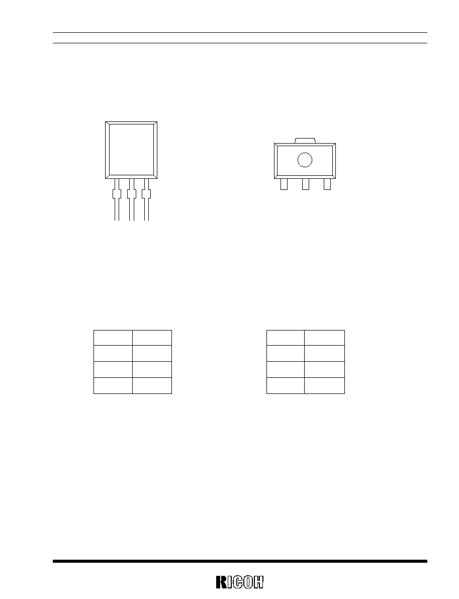
∑ TO-92
PIN CONFIGURATION
∑ SOT-89
PIN DESCRIPTION
∑ TO-92
∑ SOT-89
Pin No.
Symbol
1
GND
2
V
IN
3
V
OUT
Pin No.
Symbol
1
GND
2
V
IN
3
V
OUT
1
2
3
(mark side)
1
2
3
(mark side)
4
Rx5RE
ABSOLUTE MAXIMUM RATINGS
Symbol
Item
V
IN
Input Voltage
V
OUT
Output Voltage
I
OUT
Output Current
P
D
Power Dissipation
Topt
Operating Temperature
Tstg
Storage Temperature
Tsolder
Lead Temperature (Soldering)
Rating
Unit
+12
V
≠0.3 to V
IN
+0.3
V
300
mA
300
mW
≠40 to +85
∞C
≠55 to +25
∞C
260∞C, 10s
Absolute Maximum ratings are threshold limit values that must not be exceeded even for an instant under any
conditions. Moreover, such values for any two items must not be reached simultaneously. Operation above
these absolute maximum ratings may cause degradation or permanent damage to the device. These are stress
ratings only and do not necessarily imply functional operation below these limits.
ABSOLUTE MAXIMUM RATINGS

Rx5RE
5
ELECTRICAL CHARACTERISTICS
∑ Rx5RE20A
Symbol
Item
V
OUT
Output Voltage
I
OUT
Output Current
V
OUT
Load Regulation
I
OUT
V
DIF
Dropout Voltage
I
SS
Quiescent Current
V
OUT
V
IN
Line Regulation
V
IN
Input Voltage
Ilim
Current Limit
V
OUT
Output Voltage
Topt
Temperature Coefficient
Conditions Min.
Typ.
Max.
Unit
V
IN
=4.0V,I
OUT
=10mA
1.950
2.000
2.050
V
V
IN
=4.0V
40
60
mA
V
IN
=4.0V
1mA
I
OUT
50mA
40
80
mV
I
OUT
=30mA
0.5
0.7
V
V
IN
=4.0V
1.0
3.0
µA
I
OUT
=10mA
V
OUT
+1.0V
V
IN
10V
0.1
%/V
10
V
240
mA
I
OUT
=10mA
±100
ppm/∞C
≠40∞C
Topt85∞C
Topt=25∞C
∑ Rx5RE30A
Topt=25∞C
Symbol
Item
V
OUT
Output Voltage
I
OUT
Output Current
V
OUT
Load Regulation
I
OUT
V
DIF
Dropout Voltage
I
SS
Quiescent Current
V
OUT
V
IN
Line Regulation
V
IN
Input Voltage
Ilim
Current Limit
V
OUT
Output Voltage
Topt
Temperature Coefficient
Conditions Min.
Typ.
Max.
Unit
V
IN
=5.0V,I
OUT
=10mA
2.925
3.000
3.075
V
V
IN
=5.0V
50
80
mA
V
IN
=5.0V
1mA
I
OUT
60mA
40
80
mV
I
OUT
=40mA
0.5
0.7
V
V
IN
=5.0V
1.1
3.3
µA
I
OUT
=10mA
V
OUT
+1.0V
V
IN
10V
0.1
%/V
10
V
240
mA
I
OUT
=10mA
±100
ppm/∞C
≠40∞C
Topt85∞C

6
Rx5RE
∑
Rx5RE50A
Topt=25∞C
∑ Rx5RE40A
Topt=25∞C
Symbol
Item
V
OUT
Output Voltage
I
OUT
Output Current
V
OUT
Load Regulation
I
OUT
V
DIF
Dropout Voltage
I
SS
Quiescent Current
V
OUT
V
IN
Line Regulation
V
IN
Input Voltage
Ilim
Current Limit
V
OUT
Output Voltage
Topt
Temperature Coefficient
Conditions Min.
Typ.
Max.
Unit
V
IN
=6.0V,I
OUT
=10mA
3.900
4.000
4.100
V
V
IN
=6.0V
65
100
mA
V
IN
=6.0V
1mA
I
OUT
70mA
40
80
mV
I
OUT
=50mA
0.5
0.7
V
V
IN
=6.0V
1.2
3.6
µA
I
OUT
=10mA
V
OUT
+1.0V
V
IN
10V
0.1
%/V
10
V
240
mA
I
OUT
=10mA
±100
ppm/∞C
≠40∞C
Topt85∞C
Symbol
Item
V
OUT
Output Voltage
I
OUT
Output Current
V
OUT
Load Regulation
I
OUT
V
DIF
Dropout Voltage
I
SS
Quiescent Current
V
OUT
V
IN
Line Regulation
V
IN
Input Voltage
Ilim
Current Limit
V
OUT
Output Voltage
Topt
Temperature Coefficient
Conditions Min.
Typ.
Max.
Unit
V
IN
=7.0V,I
OUT
=10mA
4.875
5.000
5.125
V
V
IN
=7.0V
80
120
mA
V
IN
=7.0V
1mA
I
OUT
80mA
40
80
mV
I
OUT
=60mA
0.5
0.7
V
V
IN
=7.0V
1.3
3.9
µA
I
OUT
=10mA
V
OUT
+1.0V
V
IN
10V
0.1
%/V
10
V
240
mA
I
OUT
=10mA
±100
ppm/∞C
≠40∞C
Topt85∞C
Rx5RE
7
∑
Rx5RE60A
Topt=25∞C
Symbol
Item
V
OUT
Output Voltage
I
OUT
Output Current
V
OUT
Load Regulation
I
OUT
V
DIF
Dropout Voltage
I
SS
Quiescent Current
V
OUT
V
IN
Line Regulation
V
IN
Input Voltage
Ilim
Current Limit
V
OUT
Output Voltage
Topt
Temperature Coefficient
Conditions Min.
Typ.
Max.
Unit
V
IN
=8.0V,I
OUT
=10mA
5.850
6.000
6.150
V
V
IN
=8.0V
80
120
mA
V
IN
=8.0V
1mA
I
OUT
80mA
40
80
mV
I
OUT
=60mA
0.5
0.7
V
V
IN
=8.0V
1.4
4.2
µA
I
OUT
=10mA
V
OUT
+1.0V
V
IN
10V
0.1
%/V
10
V
240
mA
I
OUT
=10mA
±100
ppm/∞C
≠40∞C
Topt85∞C

8
Rx5RE
ELECTRICAL CHARACTERISTICS BY OUTPUT VOLTAGE
V
IN
≠
V
OUT
=2.0V
1mA
40
60
I
OUT
50mA
V
IN
≠
V
OUT
=2.0V
1mA
I
OUT
60mA
50
80
V
IN
≠
V
OUT
=2.0V
40
80
1mA
I
OUT
70mA
65
100
V
IN
≠
V
OUT
=2.0V
1mA
80
120
I
OUT
80mA
Rx5RE20A
1.950
2.000
2.050
Rx5RE21A
2.048
2.100
2.152
Rx5RE22A
2.145
2.200
2.255
Rx5RE23A
2.243
2.300
2.357
Rx5RE24A
2.340
2.400
2.460
Rx5RE25A
2.438
2.500
2.562
Rx5RE26A
2.535
2.600
2.665
Rx5RE27A
2.633
2.700
2.767
Rx5RE28A
2.730
2.800
2.870
Rx5RE29A
2.828
2.900
2.972
Rx5RE30A
2.925
3.000
3.075
Rx5RE31A
3.023
3.100
3.177
Rx5RE32A
3.120
3.200
3.280
Rx5RE33A
3.218
3.300
3.382
Rx5RE34A
3.315
3.400
3.485
Rx5RE35A
3.413
3.500
3.587
Rx5RE36A
3.510
3.600
3.690
Rx5RE37A
3.608
3.700
3.792
Rx5RE38A
3.705
3.800
3.895
Rx5RE39A
3.803
3.900
3.997
Rx5RE40A
3.900
4.000
4.100
Rx5RE41A
3.998
4.100
4.202
Rx5RE42A
4.095
4.200
4.305
Rx5RE43A
4.193
4.300
4.407
Rx5RE44A
4.290
4.400
4.510
Rx5RE45A
4.388
4.500
4.612
Rx5RE46A
4.485
4.600
4.715
Rx5RE47A
4.583
4.700
4.817
Rx5RE48A
4.680
4.800
4.920
Rx5RE49A
4.778
4.900
5.022
Rx5RE50A
4.875
5.000
5.125
Rx5RE51A
4.973
5.100
5.227
Rx5RE52A
5.070
5.200
5.330
Rx5RE53A
5.168
5.300
5.432
Rx5RE54A
5.265
5.400
5.535
Rx5RE55A
5.363
5.500
5.637
Rx5RE56A
5.460
5.600
5.740
Rx5RE57A
5.558
5.700
5.842
Rx5RE58A
5.655
5.800
5.945
Rx5RE59A
5.753
5.900
6.047
Rx5RE60A
5.850
6.000
6.150
Output Voltage
OutputCurrent
Load Regulation
Part Number
V
OUT
(V)
I
OUT
(mA)
V
OUT
/
I
OUT
(mV)
Conditions
Min.
Typ.
Max.
Conditions
Min.
Typ.
Conditions
Typ.
Max.
V
IN
≠
V
OUT
=2.0V
I
OUT
=10mA
V
IN
≠
V
OUT
=2.0V
I
OUT
=30mA
I
OUT
=40mA
0.5
0.7
I
OUT
=50mA
I
OUT
=60mA
Dropout Voltage
V
DIF
(V)
Conditions
Typ.
Max.
Rx5RE
9
Topt=25∞C
1.0
3.0
1.1
3.3
I
OUT
=10mA
I
OUT
V
IN
≠
=10mA
V
OUT
1.2
3.6
0.1
10
240
±100
=2.0V
V
OUT
+
≠40∞C
1.0V
Topt
V
IN
85∞C
10V
1.3
3.9
1.4
4.2
Quiescent Current
Line Regulation Input Voltage Current Limit Output Voltage Tempco.
Iss(µA)
V
OUT
/
V
I N
(%/V) V
I N
(V) Ilim(mA)
V
OUT
/
T(ppm/∞C)
Conditions
Typ.
Max.
Conditions
Typ.
Max.
Typ.
Conditions
Typ.

10
Rx5RE
OPERATION
Output voltage V
OUT
divided at the node between regis-
ters R1 and R2 is compared with reference voltage by
error amplifier, so that a constant voltage is output.
TEST CIRCUITS
FIG. 2 Test Circuit
FIG. 3 Quiescent Current Test Circuit
FIG. 4 Line Transient Response Test Circuit
FIG. 1 Brock Diagram
GND
GND
V
IN
≠
+
Error Amplifire
V
OUT
R2
R1
Vref
C
I
1
µF
Co
1
µF
V
IN
GND
Rx5RE
SERIES
V
OUT
I
OUT
V
OUT
V
IN
+
+
I
SS
C
I
1
µF
V
IN
GND
Rx5RE
SERIES
V
OUT
V
IN
+
Ro
Co
0.1
µF
P.G
GND
Rx5RE
SERIES
V
OUT
V
OUT
V
IN
+
Rx5RE
11
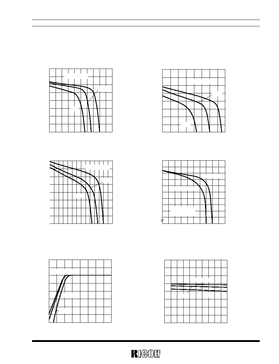
TYPICAL CHARACTERISTICS
1) Output Voltage vs. Output Current
Rx5RE40A
Rx5RE50A
Rx5RE50A
Output Current I
OUT
(mA)
Output Voltage V
OUT
(V)
0
3.7
3.8
3.9
4.1
4.0
V
IN
=6.0V
50
100
150
200
Topt=≠40∞C
85∞C
25∞C
4.7
4.8
4.9
5.1
5.0
V
IN
=7.0V
0
50
100
150
200
250
Output Voltage V
OUT
(V)
Output Current I
OUT
(mA)
with heatsink
without heatsink
4.7
4.8
4.9
5.1
5.0
V
IN
=7.0V
0
50
100
150
200
250
heatsink
30
◊
30
◊
1mm
Output Voltage V
OUT
(V)
Output Current I
OUT
(mA)
4.7
4.8
4.9
5.1
5.0
V
IN
=7.0V
0
50 100 150 200 250 300 350
25∞C
Topt=≠40∞C
85∞C
Rx5RE30A
Output Voltage V
OUT
(V)
Output Current I
OUT
(mA)
2.7
2.8
2.9
3.1
3.0
V
IN
=5.0V
0
50
100
150
200
250
Topt= ≠40∞C
25∞C
85∞C
Rx5RE20A
Rx5RE20A
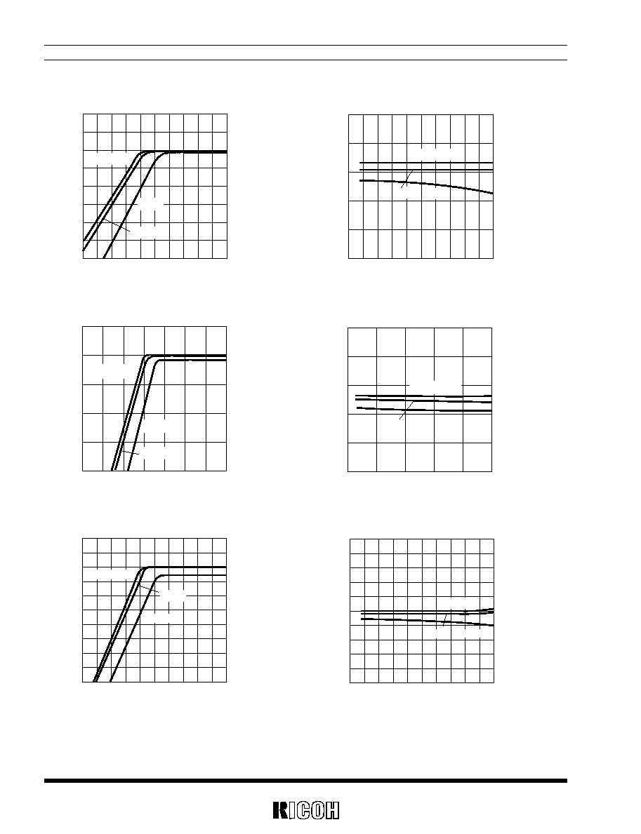
2) Output Voltage vs. Input Voltage
I
OUT
=1µA
Topt=25∞C
1.0
3.0
4.0
2.0
5.0
Input Voltage V
IN
(V)
1mA
10mA
Output Voltage V
OUT
(V)
1.0
1.2
0.8
1.4
1.6
1.8
2.0
2.2
2.4
Topt=25∞C
2
4
5
3
6
7
Input Voltage V
IN
(V)
Output Voltage V
OUT
(V)
1.98
1.96
2.00
2.02
2.04
I
OUT
=1µA
1mA
10mA
12
Rx5RE
Rx5RE30A
Rx5RE40A
Rx5RE30A
Rx5RE40A
Rx5RE50A
Rx5RE50A
Topt=25∞C
2.0
3.0
3.5
2.5
4.0
4.5
Input Voltage V
IN
(V)
Output Voltage V
OUT
(V)
2.0
2.2
1.8
2.4
2.6
2.8
3.0
3.2
3.4
I
OUT
=1mA
50mA
10mA
2.5
4.5
3.5
5.5
Input Voltage V
IN
(V)
Topt=25∞C
Output Voltage V
OUT
(V)
3.4
3.2
3.6
3.8
4.0
4.2
I
OUT
=1mA
50mA
10mA
Topt=25∞C
3.0
5.0
6.0
4.0
7.0
8.0
Input Voltage V
IN
(V)
Output Voltage V
OUT
(V)
2.96
2.95
2.97
2.98
2.99
3.00
I
OUT
=1µA
1mA
10mA
Topt=25∞C
4
6
7
5
8
9
Input Voltage V
IN
(V)
Output Voltage V
OUT
(V)
3.98
3.96
4.00
4.02
4.04
4.06
1mA
I
OUT
=1µA
10mA
Topt=25∞C
4.5
4.0
5.5
6.0
5.0
6.5
Input Voltage V
IN
(V)
Output Voltage V
OUT
(V)
4.4
4.2
4.6
4.8
5.0
5.1
I
OUT
=1mA
50mA
10mA
Topt=25∞C
6
5
8
9
7
10
Input Voltage V
IN
(V)
Output Voltage V
OUT
(V)
4.97
4.98
4.95
4.96
4.99
5.00
5.01
5.02
5.03
5.04
5.05
10mA
I
OUT
=1µA
1mA
Rx5RE
13
Rx5RE30A
Rx5RE40A
Rx5RE50A
3) Dropout Voltage vs. Output Curret
Output Current I
OUT
(mA)
Dropout Voltage V
DIF
(V)
0
20
40
60
80
100
Topt=≠40∞C
25∞C
85∞C
0.0
0.4
0.6
0.2
0.8
1.0
1.2
1.4
Output Current I
OUT
(mA)
Dropout Voltage V
DIF
(V)
0
20
40
60
80
100
85∞C
25∞C
Topt= ≠40∞C
0.0
0.4
0.5
0.7
0.6
0.2
0.3
0.1
0.8
Output Current I
OUT
(mA)
Dropout Voltage V
DIF
(V)
0
20
40
60
80
100
0.0
0.2
0.4
0.6
0.8
1.0
25∞C
Topt=≠40∞C
85∞C
Rx5RE30A
4) Output Voltage vs.Temperature
Temperature Topt(∞C)
Output Voltage V
OUT
(V)
-50 -30 -10 10
30
50
70
90
2.9
3.0
3.1
I
OUT
=10mA
Rx5RE40A
Temperature Topt(∞C)
Output Voltage V
OUT
(V)
3.9
4.0
4.1
-50 -30 -10 10
30
50
70
90
I
OUT
=10mA
14
Rx5RE
Rx5RE50A
Rx5RE20A
5) Quiescent Current vs. Input Voltage
Rx5RE40A
Rx5RE50A
Temperature Topt(∞C)
Output Voltage V
OUT
(V)
4.9
4.8
5.0
5.2
5.1
-50 -30 -10 10
30
50
70
90
I
OUT
=10mA
Input Voltage V
IN
(V)
0.6
3
4
5
6
7
8
9
10
0.7
0.8
0.9
1.0
1.1
Quiescent Current Iss(µA)
Topt=25∞C
Rx5RE30A
Input Voltage V
IN
(V)
1.0
2
4
3
5
6
7
8
9
10
1.1
1.2
1.3
1.4
Quiescent Current Iss(µA)
Topt=25∞C
Input Voltage V
IN
(V)
1.0
4
6
5
7
8
9
10
11
1.1
1.2
1.3
1.4
1.5
Quiescent Current Iss(µA)
Topt=25∞C
Input Voltage V
IN
(V)
0.5
0.6
7
6
5
8
9
10
11
12
0.7
0.8
0.9
1.0
1.1
1.2
1.3
1.5
1.4
Quiescent Current Iss(µA)
Topt=25∞C
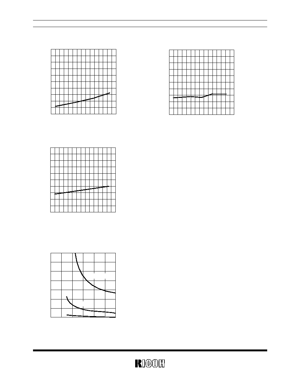
Rx5RE
15
Rx5RE20A
Rx5RE40A
6) Quiescent Current vs. Temperature
Quiescent Current Iss(
µ
A)
Temperature Topt(∞C)
0.5
0.6
0.7
0.8
0.9
1.0
1.5
1.1
1.2
1.3
1.4
≠50 ≠30 ≠10 10
30
50
70
90
Quiescent Current Iss(
µ
A)
Temperature Topt(∞C)
0.5
0.6
0.7
0.8
0.9
1.0
1.5
1.1
1.2
1.3
1.4
≠50 ≠30 ≠10
10
30
50
70
90
Rx5RE30A
Quiescent Current Iss(
µ
A)
Temperature Topt(∞C)
0.5
0.6
0.7
0.8
0.9
1.0
1.5
1.1
1.2
1.3
1.4
≠50 ≠30 ≠10
10
30
50
70
90
7) Dropout Voltage vs. Set Output Voltage
Rx5RE SERIES
0
1
2
3
4
5
6
0.0
0.2
0.1
0.3
0.4
0.5
0.6
0.7
Set Output Voltage Vreg(V)
Dropout Voltage V
DIF
(V)
1mA
Topt=25∞C
10mA
I
OUT
=50mA

16
Rx5RE
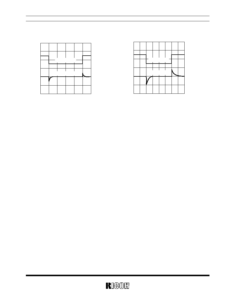
8) Line Transient Response (1)
Rx5RE30A
Rx5RE40A
Rx5RE20A
Rx5RE50A
9) Line Transient Response (2)
Rx5RE20A
Rx5RE30A
1.5
2.0
2.5
3.0
3.5
4.0
4.5
1.0
2.0
1.5
2.5
3.0
4.5
4.5
3.5
5.0
Input Voltage/Output Voltage V(V)
I
OUT
=1mA
Time t(ms)
Input Voltage
Output Voltage
1.5
2.0
2.5
3.0
3.5
4.0
4.5
2.0
4.0
3.0
5.0
7.0
6.0
8.0
Input Voltage/Output Voltage V(V)
I
OUT
=1mA
Time t(ms)
Input Voltage
Output Voltage
1.5
2.0
2.5
3.0
3.5
4.0
4.5
1.0
3.0
2.0
4.0
6.0
5.0
7.0
Input Voltage/Output Voltage V(V)
I
OUT
=1mA
Time t(ms)
Input Voltage
Output Voltage
0
0.5 1.0 1.5 2.0 2.5 3.0 3.5 4.0
Output Voltage
3.0
5.0
4.0
6.0
8.0
7.0
9.0
Input Voltage/Output Voltage V(V)
I
OUT
=1mA
Time t(ms)
Input Voltage
1.5
2.0
2.5
3.0
3.5
4.0
4.5
0.0
1.0
1.5
0.5
2.0
2.5
4.0
4.5
3.5
3.0
5.0
Input Voltage/Output Voltage V(V)
I
OUT
=30mA
Time t(ms)
Input Voltage
Output Voltage
1.5
2.0
2.5
3.0
3.5
4.0
4.5
1.0
3.0
2.0
4.0
6.0
5.0
7.0
Input Voltage/Output Voltage V(V)
I
OUT
=30mA
Time t(ms)
Input Voltage
Output Voltage
Rx5RE
17
Rx5RE40A
Rx5RE50A
1.5
2.0
2.5
3.0
3.5
4.0
4.5
2.0
4.0
3.0
5.0
7.0
6.0
8.0
Input Voltage/Output Voltage V(V)
I
OUT
=30mA
Time t(ms)
Input Voltage
Output Voltage
I
OUT
=30mA
0
0.5 1.0 1.5 2.0 2.5 3.0 3.5 4.0
Output Voltage
3.0
5.0
4.0
6.0
8.0
7.0
9.0
Input Voltage/Output Voltage V(V)
Time t(ms)
Input Voltage

18
Rx5RE
TYPICAL APPLICATION
In Rx5RE Series, a constant voltage can be obtained
without using capacitors C1 and C2. However, when the
wire connected to V
IN
is long, use capacitor C1. Output
noise can be reduced by using capacitor C2.
Insert capacitors C1 and C2 with the capacitance of
0.1µF to 2.0µF between input/output pins and GND pin
with minimum wiring.
The output voltage can be obtained by the follow-
ing formula :
V
OUT
=Vreg ∑ (1+R2/R1) + I
SS
∑ R2
Since the quiescent current of Rx5RE Series is so
small that the resistances of R1 and R2 can be set as
large as several hundreds k
and therefore the sup-
ply current of "Voltage Boost Circuit" itself can be
reduced.
Furthermore, since Rx5RE Series are operated by
a constant voltage, the supply current of "Voltage
Boost Circuit" is not substantially affected by the
input voltage.
As shown in the circuit diagram, a dual power sup-
ply circuit can be constructed by using two Rx5RE
Series.
This circuit diagram shows a dual power supply
circuit with an output of 3V and an output of 5V.
When the minimum output current of IC2 is larger
than I
SS
of IC1, resistor R is unnecessary. Diode D is
a protection diode for the case where V
OUT
2
becomes larger than V
OUT
1.
∑ VOLTAGE BOOST CIRCUIT
∑ DUAL POWER SUPPLY CIRCUIT
C2
C1
V
IN
GND
GND
GND
Rx5RE
SERIES
V
OUT
V
OUT
V
IN
+
+
C2
C1
V
IN
GND
GND
Rx5RE
SERIES
V
OUT
V
OUT
V
IN
R1
R2
I
SS
+
+
C1
C2
V
IN
GND
GND
GND
Rx5RE20A
Rx5RE30A
V
OUT
V
OUT
1
5V
V
OUT
2
3V
V
IN
C3
GND
V
OUT
V
IN
R
I
SS
IC1
IC2
D
+
+
+
*
1) Vreg : Set Output Voltage of Rx5RE Series.
*
1
APPLICATION CIRCUITS
Rx5RE
19
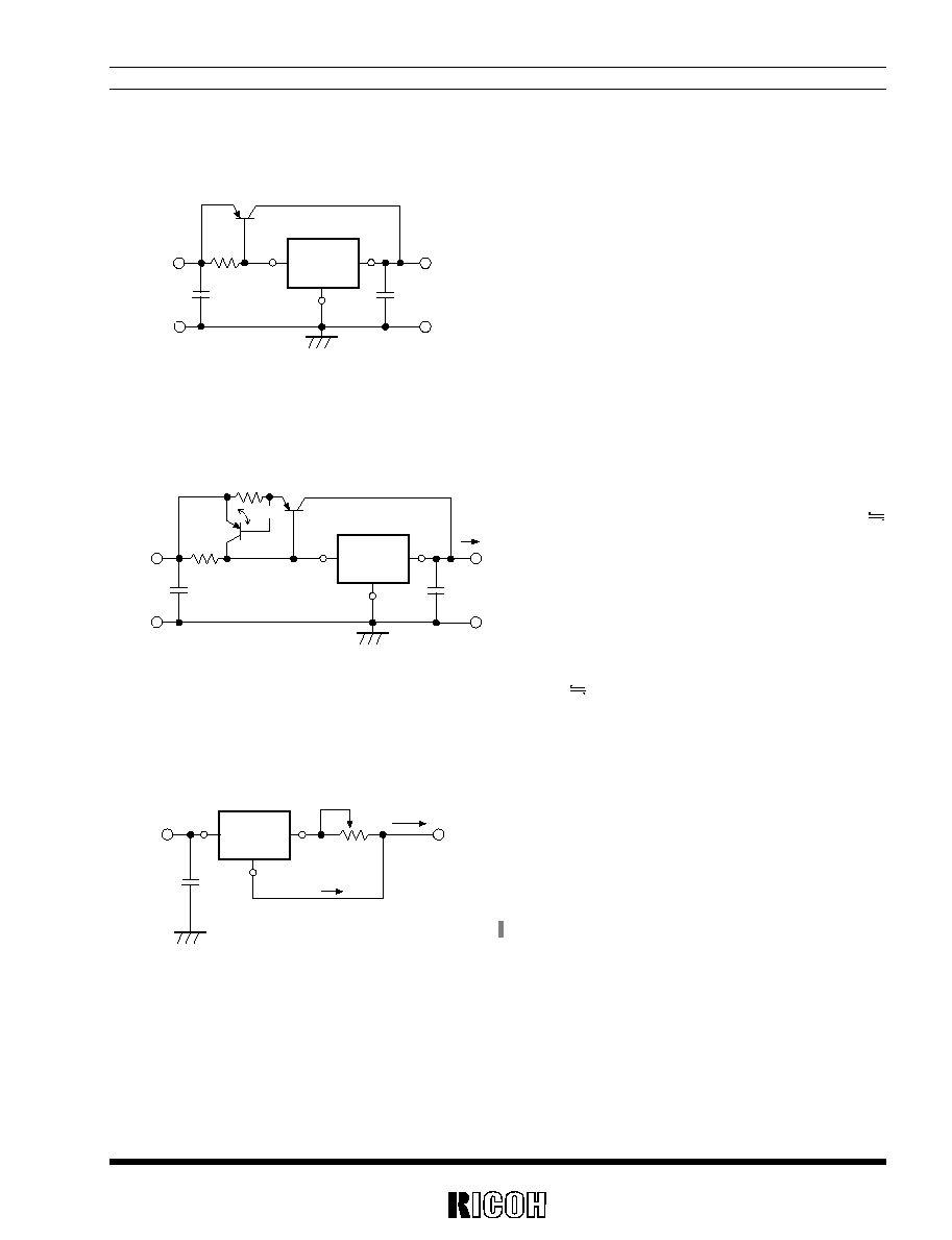
∑ CURRENT BOOST CIRCUIT
Output current of 120mA or more can be obtained
by the current boost circuit constructed as shown in
this circuit diagram.
∑ CURRENT BOOST CIRCUIT WITH OVERCURRENT LIMIT CIRCUIT
∑ CURRENT SOURCE
A current source with the structure as shown in
this circuit diagram can be used. Output Current
I
OUT
is obtained as follows :
I
OUT
=Vreg /R + I
SS
Take care that Output Current I
OUT
does not exceed
its allowable current.
C2
GND
GND
GND
Rx5RE
SERIES
V
OUT
V
OUT
C1
V
IN
V
IN
Tr.1
+
+
C2
GND
GND
GND
Rx5RE
SERIES
V
OUT
V
OUT
V
IN
V
IN
Tr.1
Tr.2
R1
R2
I
OUT
Vbe2
+
+
GND
Rx5RE
SERIES
C1
V
IN
V
IN
R
I
OUT
I
SS
V
OUT
+
A circuit for protecting Tr.1 from the destruction
caused by output short-circuit or overcurrent is shown in
this circuit diagram.
When the voltage reduction caused by the current (
aa
I
OUT
) which flows through R2 reaches Vbe2 of Tr.2 by
additionally providing the current boost circuit with Tr.2
and R2, Tr.2 is turned ON and the base current of Tr.1 is
increased, so that the output current is limited.
Current limit of Overcurrent Limit Circuit is obtained
as follows :
I
OUT
Vbe2/R2
*
1) Vreg : Set Output Voltage of Rx5RE Series.
*
1