 | –≠–ª–µ–∫—Ç—Ä–æ–Ω–Ω—ã–π –∫–æ–º–ø–æ–Ω–µ–Ω—Ç: RH5VT09A | –°–∫–∞—á–∞—Ç—å:  PDF PDF  ZIP ZIP |

ELECTRONIC DEVICES DIVISION
LOW VOLTAGE DETECTOR
R
◊
5VT SERIES
APPLICATION MANUAL
NO.EA-026-9803

NOTICE
1. The products and the product specifications described in this application manual are subject to change or dis-
continuation of production without notice for reasons such as improvement. Therefore, before deciding to use
the products, please refer to Ricoh sales representatives for the latest information thereon.
2. This application manual may not be copied or otherwise reproduced in whole or in part without prior written con-
sent of Ricoh.
3. Please be sure to take any necessary formalities under relevant laws or regulations before exporting or other-
wise taking out of your country the products or the technical information described herein.
4. The technical information described in this application manual shows typical characteristics of and example
application circuits for the products. The release of such information is not to be construed as a warranty of or a
grant of license under Ricoh's or any third party's intellectual property rights or any other rights.
5. The products listed in this document are intended and designed for use as general electronic components in
standard applications (office equipment, computer equipment, measuring instruments, consumer electronic
products, amusement equipment etc.). Those customers intending to use a product in an application requiring
extreme quality and reliability, for example, in a highly specific application where the failure or misoperation of
the product could result in human injury or death (aircraft, spacevehicle, nuclear reactor control system, traffic
control system, automotive and transportation equipment, combustion equipment, safety devices, life support
system etc.) should first contact us.
6. We are making our continuous effort to improve the quality and reliability of our products, but semiconductor
products are likely to fail with certain probability. In order prevent any injury to persons or damages to property
resulting from such failure, customers should be careful enough to incorporate safety measures in their design,
such as redundancy feature, fire-containment feature and fail-safe feature. We do not assume any liability or
responsibility for any loss or damage arising from misuse or inappropriate use of the products.
7. Anti-radiation design is not implemented in the products described in this application manual.
8. Please contact Ricoh sales representatives should you have any questions or comments concerning the prod-
ucts or the technical information.
June 1995

OUTLINE
......................................................................................................
1
FEATURES
....................................................................................................
1
APPLICATIONS
.............................................................................................
1
BLOCK DIAGRAMS
.......................................................................................
2
TIME CHART
.................................................................................................
2
DEFINITION OF OUTPUT DELAY TIME t
PLH
....................................................
2
SELECTION GUIDE
.......................................................................................
4
PIN CONFIGURATION
...................................................................................
5
PIN DESCRIPTION
........................................................................................
5
ABSOLUTE MAXIMUM RATINGS
...................................................................
6
ELECTRICAL CHARACTERISTICS
.................................................................
7
ELECTRICAL CHARACTERITICS BY DETECTOR THRESHOLD
....................
10
OPERATION
................................................................................................
14
TEST CIRCUITS
...........................................................................................
15
TYPICAL CHARACTERISTICS
......................................................................
16
1) Supply Current vs. Input Voltage
...........................................................................
16
2) Detector Threshold vs. Temperature
.......................................................................
16
3) Output Voltage vs. Input Voltage
...........................................................................
17
4) Nch Driver Output Current vs. V
DS
.........................................................................
18
5) Nch Driver Output Current vs. Input Voltage
................................................................
19
6) Pch Driver Output Current vs. Input Voltage
................................................................
20
7) Output Delay Time vs. Load Capacitance
..................................................................
20
8) Output Delay Time vs. Input Pin Capacitance
..............................................................
21
TYPICAL APPLICATIONS
............................................................................
22
∑ R
◊
5VT
◊◊
A CPU Reset Circuit(Nch Open Drain Output)
.......................................................
22
∑ R
◊
5VT
◊◊
C CPU Reset Circuit(CMOS Output)
................................................................
22
∑ R
◊
5VT
◊◊
A Output delay Time Circuit 1
.......................................................................
22
∑ R
◊
5VT
◊◊
A Output delay Time Circuit 2
.......................................................................
22
∑ Memory Back-up Circuit
.....................................................................................
22
∑ Voltage Level Indicator Circuit (lighted when the power runs out)
............................................
23
∑ Detector Threshold Changing Circuit
........................................................................
23
∑ Window Comparator Circuit
.................................................................................
23
∑ Excessive Charge Preventing Circuit
........................................................................
23
R
◊
5VT SERIES
APPLICATION MANUAL
CONTENTS

PACKAGE DIMENSIONS
.............................................................................
25
TAPING SPECIFICATIONS
...........................................................................
26

LOW VOLTAGE DETECTOR
R
◊
5VT SERIES
1
OUTLINE
The R
◊
5VT Series are voltage detector ICs with high detector threshold accuracy and ultra-low supply current
by CMOS process, which can be operated at an extremely low voltage and is used, for instance, for system reset.
Each of these ICs consists of a voltage reference unit, a comparator, resistors for voltage detection, an output
driver and a hysteresis circuit. The detector threshold is fixed with high accuracy.
The R
◊
5VT Series are operable by a lower voltage than that for the R
◊
5VL Series, and can be driven by a sin-
gle battery.
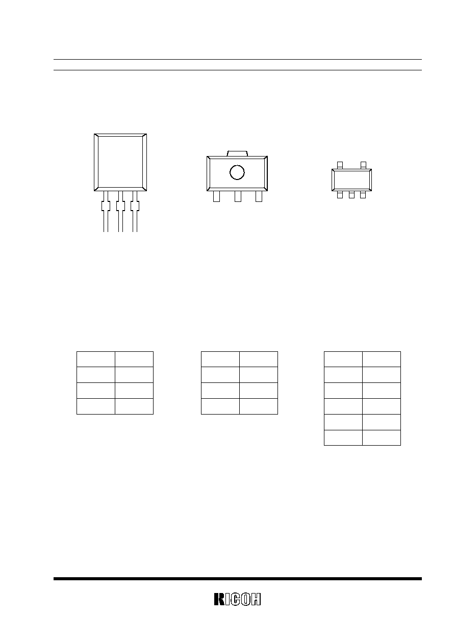
Two output types, Nch open drain type and CMOS type, are available. Three types of packages, TO-92, SOT-
89 (Mini-power Mold), SOT-23-5 (Mini-mold), are available.
∑ Ultra-low Supply Current ............................TYP. 0.8µA (V
DD
=1.5V)
∑ Broad Operating Voltage Range .................. 0.7V to 10.0V (Topt =25∞C)
∑ Detector Threshold........................................Stepwise setting with a step of 0.1V in the range of 0.9V to 6.0V
is possible (refer to Selection Guide).
∑ High Accuracy Detector Threshold..............±2.5%
∑ Low Temperature-Drift Coefficien of Detector Threshold..............TYP. ±100ppm/∞C
∑ Two Output Types.........................................Nch Open Drain and CMOS
∑ Three Types of Packages ..............................TO-92, SOT-89 (Mini-power Mold), SOT-23-5 (Mini-mold)
FEATURES
APPLICATIONS
∑
CPU & Logic Circuit Reset
∑
Battery Checker
∑
Window Comparator
∑
Wave Shaping Circuit
∑
Battery Back-Up Circuit
∑
Power Failure Detector
R
◊
5VT
2
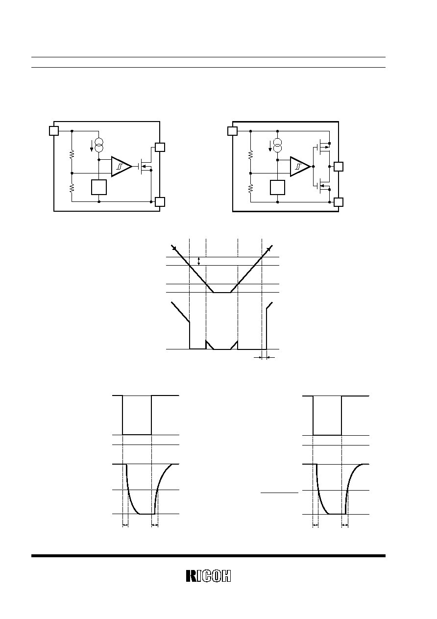
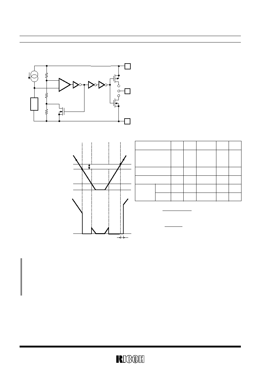
BLOCK DIAGRAMS
∑
Nch Open Drain Output (R
◊
5VT
◊◊
A)
∑
CMOS Output (R
◊
5VT
◊◊
C)
TIME CHART
DEFINITION OF OUTPUT DELAY TIME t
PLH
2
3
Vref
OUT
GND
V
DD
≠
+
1
V
DD
2
1
3
Vref
OUT
GND
≠
+
Detector Threshold Hysteresis
t
PLH
Released Voltage +V
DET
Detected Voltage ≠V
DET
Supply Voltage
(V
DD
)
Output Voltage
(OUT)
Minimum Operating Voltage
GND
GND
t
PLH
t
PHL
Input Voltage
(V
DD
)
Output Voltage
Nch Open Drain Output
GND
GND
2.5V
5.0V
0.7V
+V
DET
+ 2.0V
t
PLH
t
PHL
CMOS Output
GND
GND
0.7V
+V
DET
+ 2.0V
+V
DET
+2.0V
+V
DET
+ 2.0V
2
Input Voltage
(V
DD
)
Output Voltage

R
◊
5VT
3
Output Delay Time
t
PLH
is defined as follows:
1. In the case of Nch Open Drain Output:
When the time at which a pulse voltage which increases from 0.7V to +V
DET
+2.0V is applied to V
DD
is Time A, and
the time at which the output voltage reaches 2.5V under the conditions that the output pin (OUT) is pulled up
to 5V by a resistor of 470k
is Time B, the time period from Time A through Time B.
2. In the case of CMOS Output:
When the time at which a pulse voltage which increases from 0.7V to +V
DET
+2.0V is applied to V
DD
is Time A, and
the time at which the output voltage reaches the voltage of (+V
DET
+2.0V)/2 is Time B, the time period from
Time A through Time B.

R
◊
5VT
4
R
◊
5VT
◊◊◊◊
≠
◊◊
Part Number
a
b c d
e
}
SELECTION GUIDE
The package type, the detector threshold, the output type, the packing type, and the taping type of R
◊
5VT
series can be designating at the user's request by specifying the part number as follows:
For example, the product with Package Type SOT-89, Detector Threshold 3.5V, Output Type Nch Open Drain
and Taping Type T1, is designated by Part Number RH5VT35AA-T1.
Code
Contents
Designation of Package Type:
E: TO-92
a
H: SOT-89 (Mini-power Mold)
N: SOT-23-5 (Mini-mold)
b
Setting Detector Threshold (≠V
DET
):
Stepwise setting with a step of 0.1V in the range of 0.9V to 6.0V is possible.
Designation of Output Type:
c
A: Nch Open Drain
C: CMOS
Designation of Packing Type:
d
A: Taping
C: Antistatic bag for TO-92 and samples
Designation of Taping Type:
Ex. TO-92:
RF, RR, TZ
e
SOT-89:
T1, T2
SOT-23-5:
TR, TL
(refer to Taping Specifications)
"TZ", "T1" and "TR" are prescribed as a standard
}
R
◊
5VT
5
∑
TO-92
PIN CONFIGURATION
∑
SOT-89
∑
SOT-23-5
PIN DESCRIPTION
∑
TO-92
∑
SOT-89
∑
SOT-23-5
Pin No.
Symbol
1
OUT
2
V
DD
3
GND
4
NC
5
NC
Pin No.
Symbol
1
OUT
2
V
DD
3
GND
Pin No.
Symbol
1
OUT
2
V
DD
3
GND
1
2
3
(mark side)
1
2
3
(mark side)
1
2
3
(mark side)
5
4
6
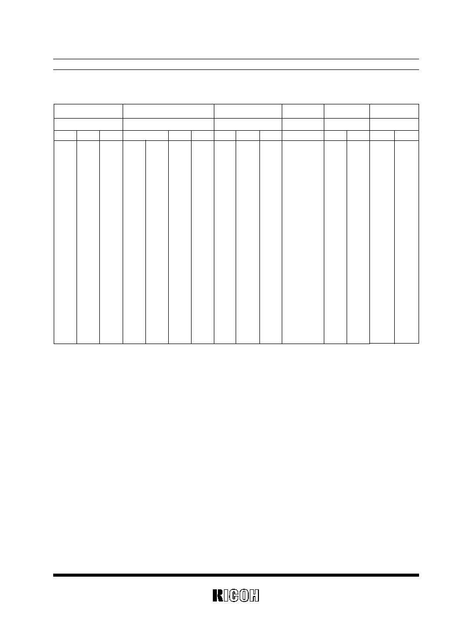
ABSOLUTE MAXIMUM RATINGS
Symbol
Item
V
DD
Supply Voltage
V
OUT
Output Voltage
I
OUT
Output Current
P
D
1
Power Dissipation 1
(
NOTE
1)
P
D
2
Power Dissipation 2
(
NOTE
2)
Topt
Operating Temperature Range
Tstg
Storage Temperature Range
Tsolder
Lead Temperature (Soldering)
Rating
Unit
12
V
CMOS
V
SS
≠0.3 to V
DD
+0.3
V
Nch
V
SS
≠0.3 to 12
70
mA
300
mW
150
mW
≠30 to +80
∞C
≠55 to +125
∞C
260∞C,10s
Topt=25∞C
(NOTE 1) applied to SOT-89 and TO-92
(NOTE 2) applied to SOT-23-5
Absolute Maximum ratings are threshold limit values that must not be exceeded even for an instant under any
conditions. Moreover, such values for any two items must not be reached simultaneously. Operation above
these absolute maximum ratings may cause degradation or permanent damage to the device. These are stress
ratings only and do not necessarily imply functional operation below these limits.
ABSOLUTE MAXIMUM RATINGS
R
◊
5VT
7
∑
R
◊
5VT18A/C
Topt=25∞C
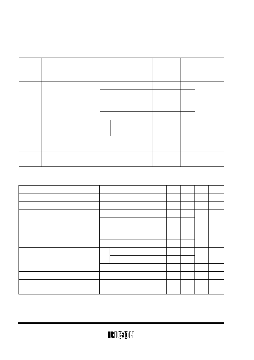
ELECTRICAL CHARACTERISTICS
∑
R
◊
5VT09A/C
Symbol
Item
≠V
DET
Detector Threshold
V
HYS
Detector Threshold Hysteresis
I
SS
Supply Current
V
DDH
Maximum Operating Voltage
V
DDL
Minimum Operating Voltage
I
OUT
Output Current
t
PLH
Output Delay Time
≠V
DET
Detector Threshold
Topt
Temperature Coefficient
Conditions
MIN.
TYP.
MAX.
Unit
Note
0.878
0.900
0.922
V
0.027
0.045
0.063
V
V
DD
=0.80V
0.8
2.4
V
DD
=2.90V
0.9
2.7
µA
10
V
Topt=25∞C
0.55
0.70
V
Note 1
≠30∞C
Topt
80∞C
0.65
0.80
Nch
V
DS
=0.05V,V
DD
=0.70V
0.01
0.05
mA
V
DS
=0.50V,V
DD
=0.85V
0.05
0.50
Pch V
DS
=≠2.1V,V
DD
=4.5V
1.0
2.0
mA
100
µs
Note 2
≠30∞C
Topt
80∞C
±100
ppm/∞C
Topt=25∞C
Symbol
Item
≠V
DET
Detector Threshold
V
HYS
Detector Threshold Hysteresis
I
SS
Supply Current
V
DDH
Maximum Operating Voltage
V
DDL
Minimum Operating Voltage
I
OUT
Output Current
t
PLH
Output Delay Time
≠V
DET
Detector Threshold
Topt
Temperature Coefficient
Conditions
MIN.
TYP.
MAX.
Unit
Note
1.755
1.800
1.845
V
0.054
0.090
0.126
V
V
DD
=1.70V
0.8
2.4
V
DD
=3.80V
1.0
3.0
µA
10
V
Topt=25∞C
0.55
0.70
V
Note 1
≠30∞C
Topt
80∞C
0.65
0.80
Nch
V
DS
=0.05V,V
DD
=0.70V
0.01
0.05
mA
V
DS
=0.50V,V
DD
=1.50V
1.00
2.00
Pch V
DS
=≠2.1V,V
DD
=4.5V
1.0
2.0
mA
100
µs
Note 2
≠30∞C
Topt
80∞C
±100
ppm/∞C
R
◊
5VT
8
Topt=25∞C
∑
R
◊
5VT27A/C
Topt=25∞C
Symbol
Item
≠V
DET
Detector Threshold
V
HYS
Detector Threshold Hysteresis
I
SS
Supply Current
V
DDH
Maximum Operating Voltage
V
DDL
Minimum Operating Voltage
I
OUT
Output Current
t
PLH
Output Delay Time
≠V
DET
Detector Threshold
Topt
Temperature Coefficient
Conditions
MIN.
TYP.
MAX.
Unit
Note
2.633
2.700
2.767
V
0.081
0.135
0.189
V
V
DD
=2.60V
0.9
2.7
V
DD
=4.70V
1.1
3.3
µA
10
V
Topt=25∞C
0.55
0.70
V
Note 1
≠30∞C
Topt
80∞C
0.65
0.80
Nch
V
DS
=0.05V,V
DD
=0.70V
0.01
0.05
mA
V
DS
=0.50V,V
DD
=1.50V
1.00
2.00
Pch V
DS
=≠2.1V,V
DD
=4.5V
1.0
2.0
mA
100
µs
Note 2
≠30∞C
Topt
80∞C
±100
ppm/∞C
Symbol
Item
≠V
DET
Detector Threshold
V
HYS
Detector Threshold Hysteresis
I
SS
Supply Current
V
DDH
Maximum Operating Voltage
V
DDL
Minimum Operating Voltage
I
OUT
Output Current
t
PLH
Output Delay Time
≠V
DET
Detector Threshold
Topt
Temperature Coefficient
Conditions
MIN.
TYP.
MAX.
Unit
Note
3.510
3.600
3.690
V
0.108
0.180
0.252
V
V
DD
=3.47V
1.0
3.0
V
DD
=5.60V
1.2
3.6
µA
10
V
Topt=25∞C
0.55
0.70
V
Note 1
≠30∞C
Topt
80∞C
0.65
0.80
Nch
V
DS
=0.05V,V
DD
=0.70V
0.01
0.05
mA
V
DS
=0.50V,V
DD
=1.50V
1.00
2.00
Pch V
DS
=≠2.1V,V
DD
=4.5V
1.0
2.0
mA
100
µs
Note 2
≠30∞C
Topt
80∞C
±100
ppm/∞C

R
◊
5VT
9
∑
R
◊
5VT54A/C
Topt=25∞C
(Note 1) Minimum Operating Voltage means the value of input voltage when output voltage maintains 0.1V or less, provided that in the case of
Nch Open Drain Type Products, the pull-up resistance is set at 470k
, and the pull-up voltage is set at 5.0V.
(Note 2) Refer to the previously defined "Output Delay Time
t
PLH
".
∑
R
◊
5VT45A/C
Topt=25∞C
Symbol
Item
≠V
DET
Detector Threshold
V
HYS
Detector Threshold Hysteresis
I
SS
Supply Current
V
DDH
Maximum Operating Voltage
V
DDL
Minimum Operating Voltage
I
OUT
Output Current
t
PLH
Output Delay Time
≠V
DET
Detector Threshold
Topt
Temperature Coefficient
Conditions
MIN.
TYP.
MAX.
Unit
Note
4.388
4.500
4.612
V
0.135
0.225
0.315
V
V
DD
=4.34V
1.1
3.3
V
DD
=6.50V
1.3
3.9
µA
10
V
Topt=25∞C
0.55
0.70
V
Note 1
≠30∞C
Topt
80∞C
0.65
0.80
Nch
V
DS
=0.05V,V
DD
=0.70V
0.01
0.05
mA
V
DS
=0.50V,V
DD
=1.50V
1.00
2.00
Pch V
DS
=≠2.1V,V
DD
=8.0V
1.5
3.0
mA
100
µs
Note 2
≠30∞C
Topt
80∞C
±100
ppm/∞C
Symbol
Item
≠V
DET
Detector Threshold
V
HYS
Detector Threshold Hysteresis
I
SS
Supply Current
V
DDH
Maximum Operating Voltage
V
DDL
Minimum Operating Voltage
I
OUT
Output Current
t
PLH
Output Delay Time
≠V
DET
Detector Threshold
Topt
Temperature Coefficient
Conditions
MIN.
TYP.
MAX.
Unit
Note
5.265
5.400
5.535
V
0.162
0.270
0.378
V
V
DD
=5.20V
1.2
3.6
V
DD
=7.40V
1.4
4.2
µA
10
V
Topt=25∞C
0.55
0.70
V
Note 1
≠30∞C
Topt
80∞C
0.65
0.80
Nch
V
DS
=0.05V,V
DD
=0.70V
0.01
0.05
mA
V
DS
=0.50V,V
DD
=1.50V
1.00
2.00
Pch V
DS
=≠2.1V,V
DD
=8.0V
1.5
3.0
mA
100
µs
Note 2
≠30∞C
Topt
80∞C
±100
ppm/∞C
R
◊
5VT
10
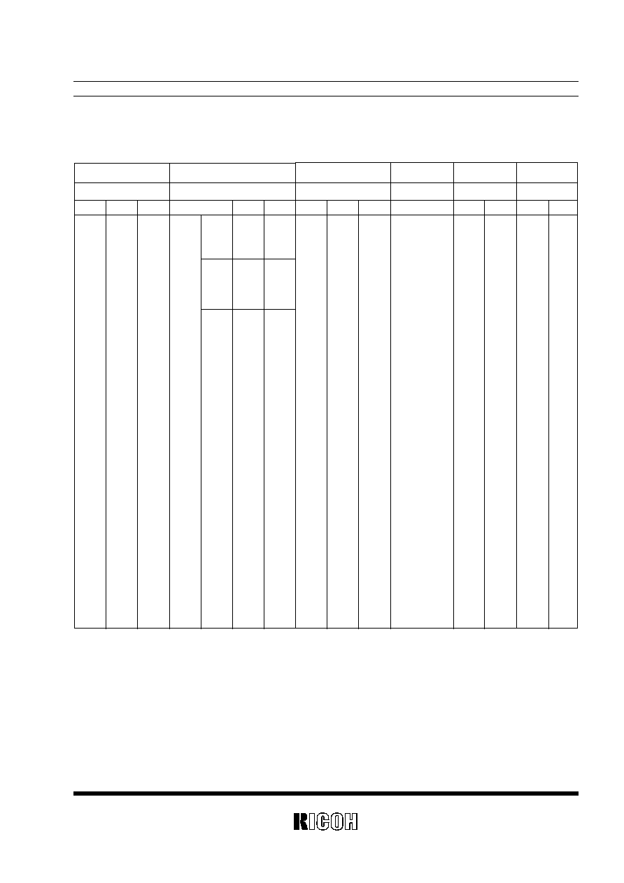
Supply Current 1
Supply Current 2
Iss(µA)
Iss(µA)
Conditions
TYP.
MAX.
Conditions
TYP.
MAX.
0.9
2.7
0.8
2.4
1.0
3.0
V
DD
=
(≠V
DET
)
≠0.10V
V
DD
=
0.9
2.7
(≠V
DET
)
1.1
3.3
+2.0V
V
DD
=
(≠V
DET
)
1.0
3.0
1.2
3.6
≠0.13V
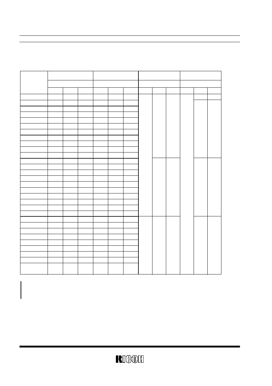
∑
R
◊
5VT09A/C to R
◊
5VT39A/C
Detector Threshold
Detector Threshold
Part Number
≠V
DET
(V)
V
HYS
(V)
MIN.
TYP.
MAX.
MIN.
TYP.
MAX.
R
◊
5VT09A/C
0.878
0.900
0.922
0.027
0.045
0.063
R
◊
5VT10A/C
0.975
1.000
1.025
0.030
0.050
0.070
R
◊
5VT11A/C
1.073
1.100
1.127
0.033
0.055
0.077
R
◊
5VT12A/C
1.170
1.200
1.230
0.036
0.060
0.084
R
◊
5VT13A/C
1.268
1.300
1.332
0.039
0.065
0.091
R
◊
5VT14A/C
1.365
1.400
1.435
0.042
0.070
0.098
R
◊
5VT15A/C
1.463
1.500
1.537
0.045
0.075
0.105
R
◊
5VT16A/C
1.560
1.600
1.640
0.048
0.080
0.112
R
◊
5VT17A/C
1.658
1.700
1.742
0.051
0.085
0.119
R
◊
5VT18A/C
1.755
1.800
1.845
0.054
0.090
0.126
R
◊
5VT19A/C
1.853
1.900
1.947
0.057
0.095
0.133
R
◊
5VT20A/C
1.950
2.000
2.050
0.060
0.100
0.140
R
◊
5VT21A/C
2.048
2.100
2.152
0.063
0.105
0.147
R
◊
5VT22A/C
2.145
2.200
2.255
0.066
0.110
0.154
R
◊
5VT23A/C
2.243
2.300
2.357
0.069
0.115
0.161
R
◊
5VT24A/C
2.340
2.400
2.460
0.072
0.120
0.168
R
◊
5VT25A/C
2.438
2.500
2.562
0.075
0.125
0.175
R
◊
5VT26A/C
2.535
2.600
2.665
0.078
0.130
0.182
R
◊
5VT27A/C
2.633
2.700
2.767
0.081
0.135
0.189
R
◊
5VT28A/C
2.730
2.800
2.870
0.084
0.140
0.196
R
◊
5VT29A/C
2.828
2.900
2.972
0.087
0.145
0.203
R
◊
5VT30A/C
2.925
3.000
3.075
0.090
0.150
0.210
R
◊
5VT31A/C
3.023
3.100
3.177
0.093
0.155
0.217
R
◊
5VT32A/C
3.120
3.200
3.280
0.096
0.160
0.224
R
◊
5VT33A/C
3.218
3.300
3.382
0.099
0.165
0.231
R
◊
5VT34A/C
3.315
3.400
3.485
0.102
0.170
0.238
R
◊
5VT35A/C
3.413
3.500
3.587
0.105
0.175
0.245
R
◊
5VT36A/C
3.510
3.600
3.690
0.108
0.180
0.252
R
◊
5VT37A/C
3.608
3.700
3.792
0.111
0.185
0.259
R
◊
5VT38A/C
3.705
3.800
3.895
0.114
0.190
0.266
Hysteresis
ELECTRICAL CHARACTEISTICS BY DETECTOR THRESHOLD
(Note 1) Refer to the previously defined "Output Delay Time
t
PLH
".
(Note 2) Refer to the previously defined "Minimum Operating Voltage".
Condition 1:Topt =25∞C
Condition 2:≠30∞C
Topt
80∞C
11
Output Current 1
Output Current 2
I
OUT
(mA)
I
OUT
(mA)
Conditions
MIN.
TYP.
Conditions
MIN.
TYP.
V
DD
=
0.05
0.50
0.85V
V
DD
=
0.2
1.0
1.0V
Nch
V
DS
=
V
DS
=
0.05V
0.01
0.05
0.50V
V
DD
=
1.5V
1.0
2.0
V
DD
=
0.7V
Output Current 3
Output Delay
Minimum
I
OUT
(mA)
t
PLH
(µs)
V
DDL
(V)
Conditions
MIN.
TYP.
MAX.
TYP.
MAX.
Pch
Note 2 Note 2
V
DS
=
Note 1
Condition 1 Condition 1
≠2.1V
1.0
2.0
100
0.55
0.70
V
DD
=
Condition 2 Condition 2
4.5V
0.65
0.80
Detector Threshold
Conditions
TYP.
≠30∞C
Topt
±100
80∞C
Time
Operating Voltage
Tempco.
≠V
DET
/
Topt
(ppm/∞C)
Topt=25∞C
R
◊
5VT
12
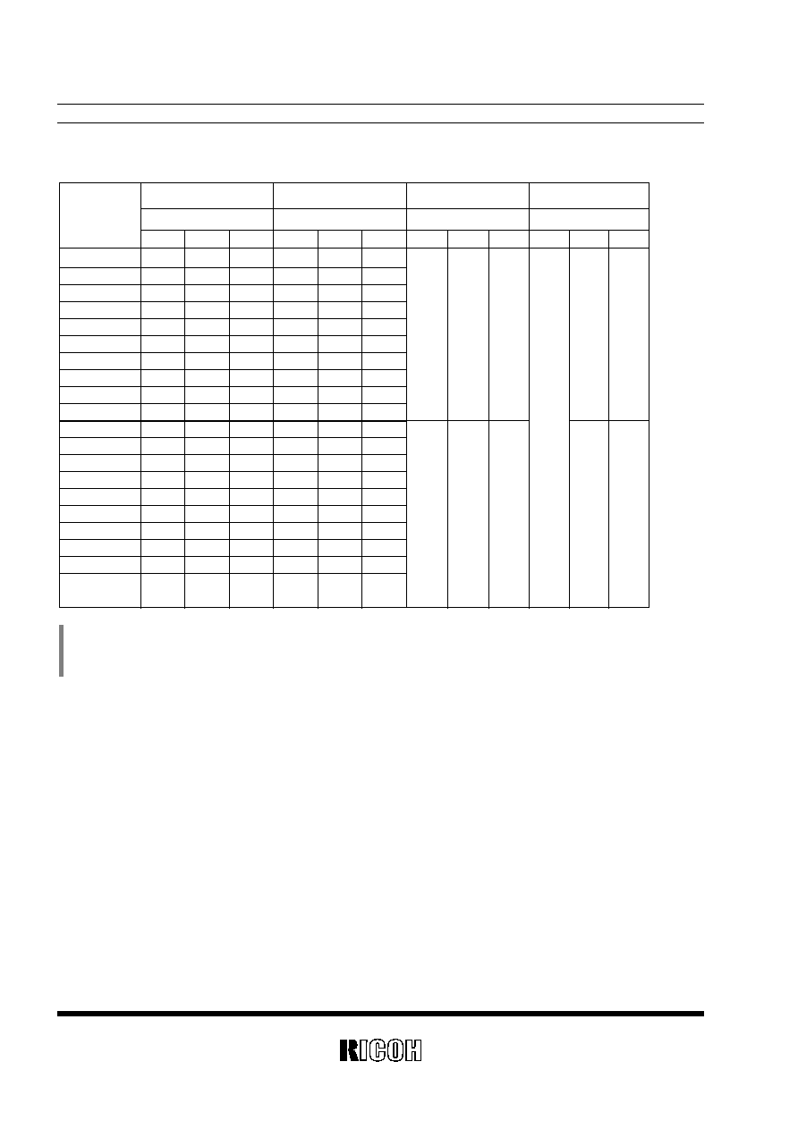
Supply Current 1
Supply Current 2
I
SS
(µA)
I
SS
(µA)
Conditions
TYP.
MAX.
Conditions
TYP.
MAX.
V
DD
=
(≠V
DET
)
1.1
3.3
1.3
3.9
≠0.16V
V
DD
=
(≠V
DET
)
+2.0V
V
DD
=
(≠V
DET
)
1.2
3.6
1.4
4.2
≠0.20V
Detector Threshold
Detector Threshold
Part Number
≠V
DET
(V)
V
HYS
(V)
MIN.
TYP.
MAX.
MIN.
TYP.
MAX.
R
◊
5VT40A/C
3.900
4.000
4.100
0.120
0.200
0.280
R
◊
5VT41A/C
3.998
4.100
4.202
0.123
0.205
0.287
R
◊
5VT42A/C
4.095
4.200
4.305
0.126
0.210
0.294
R
◊
5VT43A/C
4.193
4.300
4.407
0.129
0.215
0.301
R
◊
5VT44A/C
4.290
4.400
4.510
0.132
0.220
0.308
R
◊
5VT45A/C
4.388
4.500
4.612
0.135
0.225
0.315
R
◊
5VT46A/C
4.485
4.600
4.715
0.138
0.230
0.322
R
◊
5VT47A/C
4.583
4.700
4.817
0.141
0.235
0.329
R
◊
5VT48A/C
4.680
4.800
4.920
0.144
0.240
0.336
R
◊
5VT49A/C
4.778
4.900
5.022
0.147
0.245
0.343
R
◊
5VT50A/C
4.875
5.000
5.125
0.150
0.250
0.350
R
◊
5VT51A/C
4.973
5.100
5.277
0.153
0.255
0.357
R
◊
5VT52A/C
5.070
5.200
5.330
0.156
0.260
0.364
R
◊
5VT53A/C
5.168
5.300
5.432
0.159
0.265
0.371
R
◊
5VT54A/C
5.265
5.400
5.535
0.162
0.270
0.378
R
◊
5VT55A/C
5.363
5.500
5.637
0.165
0.275
0.385
R
◊
5VT56A/C
5.460
5.600
5.740
0.168
0.280
0.392
R
◊
5VT57A/C
5.558
5.700
5.842
0.171
0.285
0.399
R
◊
5VT58A/C
5.655
5.800
5.945
0.174
0.290
0.406
R
◊
5VT59A/C
5.753
5.900
6.047
0.177
0.295
0.413
Hysteresis
(Note 1) Refer to the previously defined "Output Delay Time t
PLH
".
(Note 2) Refer to the previously defined "Minimum Operating Voltage".
Condition 1:Topt =25∞C
Condition 2:≠30∞C
Topt
80∞C
∑
R
◊
5VT40A/C to R
◊
5VT60A/C
13
Output Current 1
Output Current 2
I
OUT
(mA)
I
OUT
(mA)
Conditions
MIN.
TYP.
Conditions
MIN.
TYP.
Nch
V
DS
=
V
DS
=
V
DD
=
0.05V
0.01
0.05
0.50V
1.5V
1.0
2.0
V
DD
=
0.7V
Output Current 3
Output Delay
Minimum
I
OUT
(mA)
t
PLH
(µs)
V
DDL
(V)
Conditions
MIN.
TYP.
MAX.
TYP.
MAX.
Pch
Note 2 Note 2
V
DS
=
Note 1
Condition 1 Condition 1
≠2.1V
1.5
3.0
100
0.55
0.70
V
DD
=
Condition 2 Condition 2
8.0V
0.65
0.80
Detector Threshold
Conditions
TYP.
≠30∞C
Topt
±100
80∞C
Time
Operating Voltage
Tempco.
≠V
DET
/
Topt
(ppm/∞C)
Topt=25∞C
14
OPERATION
FIG. 1 Block Diagram
Operation Diagram
Step 1. Output Voltage is equal to Power Source Voltage (V
DD
).
Step 2. When Input Voltage to Comparator reaches the state of Vref
V
DD
∑(Rb+Rc)/(Ra+Rb+Rc)at Point A (Detected Voltage ≠V
DET
), the output of Com-
parator is reserved, so that Output Voltage becomes GND.
Step 3. In the case of CMOS Output, Output Voltage becomes unstable when Supply Voltage (V
DD
) is smaller than Minimum Operating Voltage. In the
case of Nch Open Drain Output, a pulled-up voltage is output.
Step 4. Output Voltage becomes equal to GND.
Step 5. When Input Voltage to Comparator reaches the state of Vref
V
DD
∑ (Rb)/(Ra+ Rb) at Point B (Released Voltage +V
DET
), the output of Comparator is reversed,
so that Output Voltage becomes equal to Supply Voltage (V
DD
).
FIG. 2 Operation Diagram
Step
Step 1
Step 2
Step 3
Step 4
Step 5
Comparator(+) Pin
Input Voltage
I
II
II
II
I
Comparator Output
H
L
Indefinite
L
H
Tr. 1
OFF
ON
Indefinite
ON
OFF
Output Tr.
Pch
ON
OFF
Indefinite
OFF
ON
Nch
OFF
ON
Indefinite
ON
OFF
I
.
Rb + Rc
Ra + Rb + Rc
∑V
DD
II.
Rb
Ra + Rb
∑V
DD
GND
OUT
V
DD
Ra
Rb
Rc
Tr.1
V
r
e
f
Pch
Nch
≠
+
Detector Threshold Hysteresis
t
PLH
1
2
3
4
5
A
B
∑ In R
◊
5VT
◊◊
A, Nch Tr. drain is
connected to OUT pin.
∑ In R
◊
5VT
◊◊
C, Nch Tr. drain
and Pch Tr. drain are connected
to OUT pin.
Released Volage +V
DET
Supply Volage
Detected Volage ≠V
DET
(V
DD
)
Minimum Operating Volage
GND
Output Volage
(OUT)
GND
15
R
◊
5VT
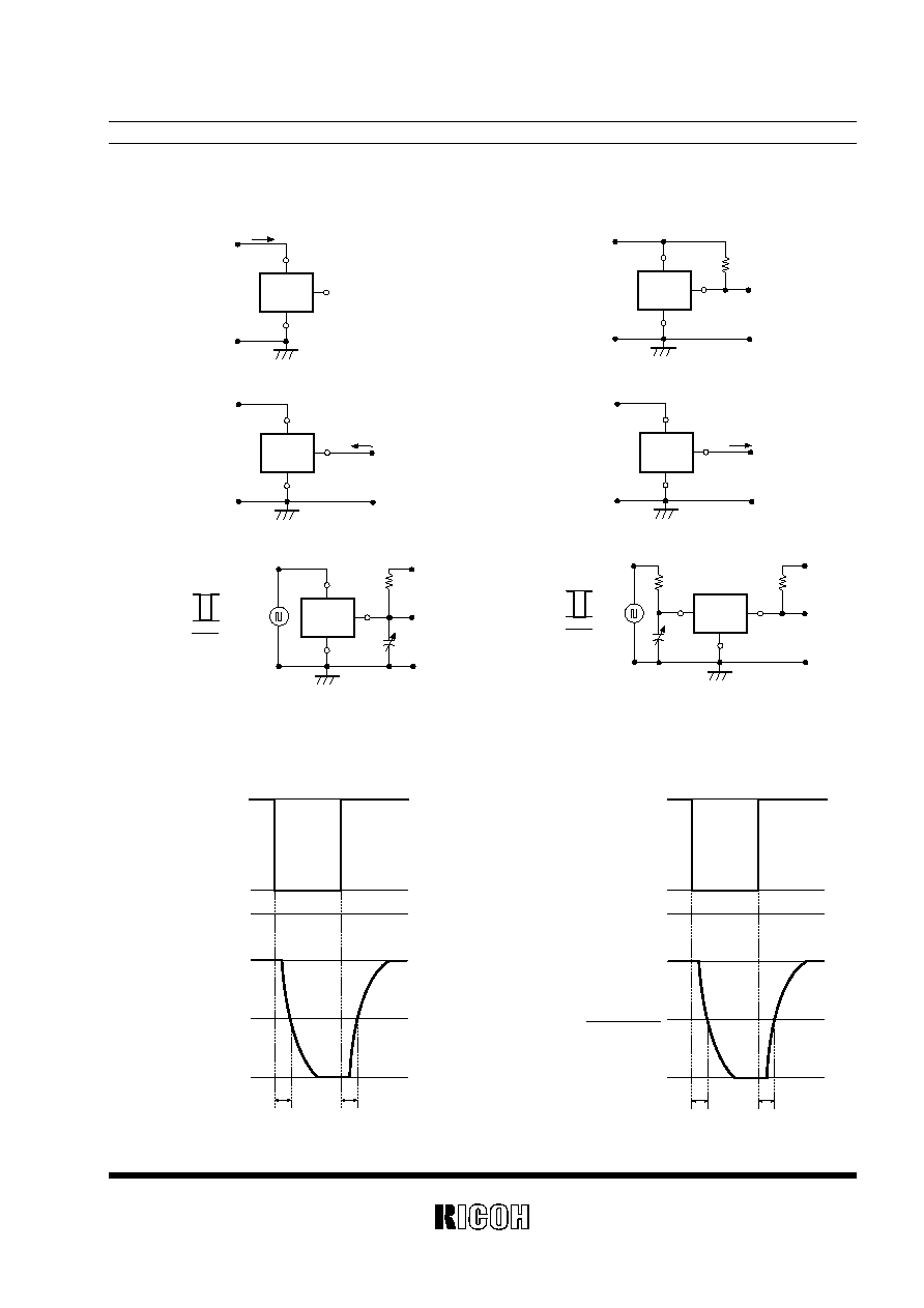
TEST CIRCUITS
FIG. 3 Supply Current Test Circuit
FIG. 5 Nch Driver Output Current Test Circuit
FIG. 4 Detector Threshold Test Circuit
FIG. 6 Pch Driver Output Current Test Circuit
FIG. 7 Output Delay Time Test Circuit
(
1
)
FIG. 8 Output Delay Time Test Circuit
(
2
)
In Output Delay Time Test Circuits (1) and (2) in FIG. 7 and FIG. 8, their respective Output Voltage Fall Times
(t
PHL
) and Rise Times (t
PLH
) are defined as shown below.
V
DD
VSS
I
SS
V
DD
GND
OUT
R
◊
5VT
SERIES
VDD
VSS
V
DD
GND
OUT
R
◊
5VT
SERIES
Rn
VSS
V
DET
Rn:R
◊
5VT
◊◊
A:470k
R
◊
5VT
◊◊
C:None
V
DD
VSS
V
DD
GND
OUT
R
◊
5VT
SERIES
I
OUT
VSS
+V
DS
V
DD
R
◊
5VT
◊◊
C
SERIES
VSS
V
DD
GND
OUT
I
OUT
VSS
V
DD
≠V
DS
P.G.
R
◊
5VT
◊◊
A
SERIES
V
DD
GND
OUT
OUT
VSS
C
OUT
+5.0V
R
OUT
470k
+V
DET
+2.0V
0.7V
VSS
R
◊
5VT
◊◊
A
SERIES
V
DD
GND
OUT
OUT
VSS
+5.0V
+V
DET
+2.0V
R
OUT
470k
100k
0.7V
VSS
P.G.
R
IN
C
IN
t
PHL
t
PLH
+V
DET
+2.0V
Input Voltage
Output Voltage
0.7V
GND
5.0V
2.5V
GND
Nch Open Drain Output
t
PHL
t
PLH
+V
DET
+2.0V
+V
DET
+2.0V
+V
DET
+2.0V
GND
0.7V
GND
2
CMOS Output
Input Voltage
Output Voltage
R
◊
5VT
16
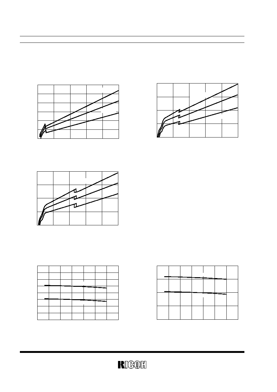
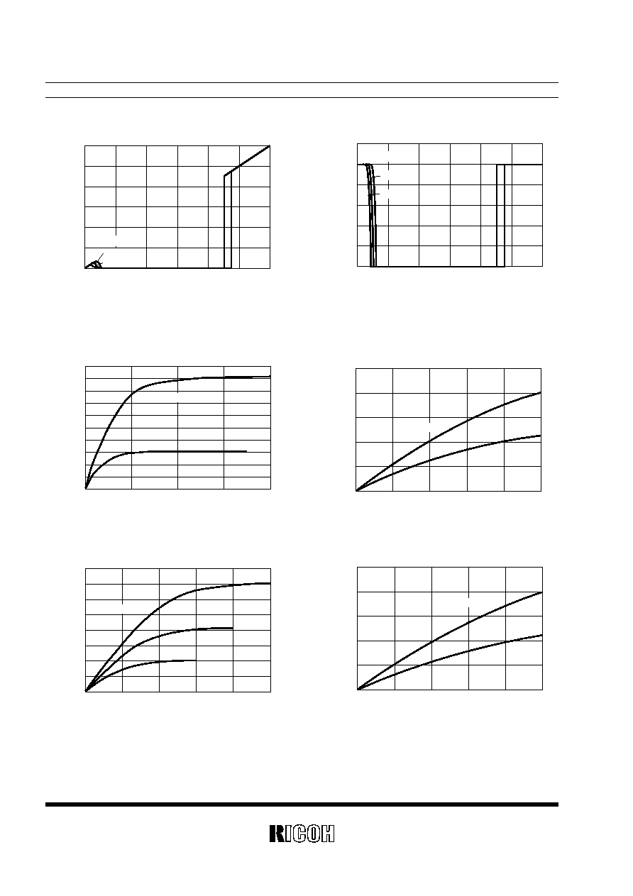
TYPICAL CHARACTERISTICS
1) Supply Current vs. Input Voltage
R
◊
5VT09C
R
◊
5VT27C
R
◊
5VT45C
R
◊
5VT09C
R
◊
5VT27C
0
0
0.5
1.0
1.5
2.0
2.5
3.0
2
4
6
8
10
Input Voltage V
IN
(V)
S
u
p
p
l
y
C
u
r
r
e
n
t
I
S
S
(
µ
A
)
Topt=80∞C
25∞C
≠30∞C
0
0
0.5
1.0
1.5
2.0
2
4
6
8
10
Input Voltage V
IN
(V)
S
u
p
p
l
y
C
u
r
r
e
n
t
I
S
S
(
µ
A
)
Topt=80∞C
≠30∞C
25∞C
≠30∞C
0
0
0.5
1.0
1.5
2.0
2.5
3.0
2
4
6
8
10
Input Voltage V
IN
(V)
S
u
p
p
l
y
C
u
r
r
e
n
t
I
S
S
(
µ
A
)
Topt=80∞C
25∞C
≠40
0.84
0.86
0.88
0.90
0.92
0.94
0.96
0.98
1.00
≠20
0
20
40
60
80
100
Tenperature Topt(∞C)
D
e
t
e
c
t
o
r
T
h
r
e
s
h
o
l
d
V
D
E
T
(
V
)
+V
DET
≠V
DET
≠40
2.5
2.6
2.7
2.8
2.9
≠20
0
20
40
60
80
100
Temperature Topt(∞C)
D
e
t
e
c
t
o
r
T
h
r
e
s
h
o
l
d
V
D
E
T
(
V
)
+V
DET
≠V
DET
2) Detector Threshold vs. Temperature

R
◊
5VT
17
R
◊
5VT45C
R
◊
5VT09A
R
◊
5VT09A
R
◊
5VT27A
3) Output Voltage vs. Input Voltage
R
◊
5VT27A
≠40
4.4
4.5
4.6
4.7
4.8
≠20
0
20
40
60
80
100
Temperature Topt(∞C)
D
e
t
e
c
t
o
r
T
h
r
e
s
h
o
l
d
V
D
E
T
(
V
)
+V
DET
≠V
DET
0
0.2
0.4
0.6
0.8
1.0
1.2
1.4
1.6
0
0.2
0.4
0.6
0.8
1.0
1.2
1.4
1.6
Input Voltage V
IN
(V)
V
DD
Pull-up 470k
O
u
t
p
u
t
V
o
l
t
a
g
e
V
O
U
T
(
V
)
25∞C
80∞C
Topt=≠30∞C
80∞C
0
0.2
0.4
0.6
0.8
1.0
1.2
1.4
1.6
0
1
2
3
4
5
6
Input Voltage V
IN
(V)
5V Pull-up 470k
O
u
t
p
u
t
V
o
l
t
a
g
e
V
O
U
T
(
V
)
25∞C
Topt=≠30∞C
0
0.5
1.0
1.5
2.0
2.5
3.0
3.5
4.0
0
2
1
3
4
Input Voltage V
IN
(V)
V
DD
Pull-up 470k
O
u
t
p
u
t
V
o
l
t
a
g
e
V
O
U
T
(
V
)
25∞C
80∞C
Topt=≠30∞C
0
0.5
1.0
1.5
2.0
2.5
3.0
3.5
4.0
0
1
2
3
4
5
6
Input Voltage V
IN
(V)
5V Pull-up 470k
O
u
t
p
u
t
V
o
l
t
a
g
e
V
O
U
T
(
V
)
25∞C
Topt=≠30∞C
80∞C
R
◊
5VT
18
4) Nch Driver Output Current vs. V
DS
R
◊
5VT45A
R
◊
5VT45A
R
◊
5VT09C
R
◊
5VT27C
R
◊
5VT27C
R
◊
5VT09C
0
0
1
2
3
4
5
6
1
2
3
4
5
6
Input Voltage V
IN
(V)
O
u
t
p
u
t
V
o
l
t
a
g
e
V
O
U
T
(
V
)
Topt=≠30∞C
25∞C
80∞C
V
DD
Pull-up 470k
0
0
1
2
3
4
5
6
1
2
3
4
5
6
Input Voltage V
IN
(V)
O
u
t
p
u
t
V
o
l
t
a
g
e
V
O
U
T
(
V
)
Topt=≠30∞C
25∞C
80∞C
5V Pull-up 470k
0
0
0.05
0.10
0.15
0.20
0.25
0.30
0.35
0.40
0.45
0.50
0.2
0.4
0.6
0.8
V
DS
(V)
Topt=25∞C
O
u
t
p
u
t
C
u
r
r
e
n
t
I
O
U
T
(
m
A
)
V
DD
=0.85V
0.7V
0
0
0.05
0.10
0.15
0.20
0.25
0.02
0.04
0.06
0.08
0.10
V
DS
(V)
Topt=25∞C
O
u
t
p
u
t
C
u
r
r
e
n
t
I
O
U
T
(
m
A
)
V
DD
=0.8V
0.7V
2.0V
1.5V
0
0.5
1.0
1.5
2.0
2.5
0
2
4
6
8
10
12
14
16
V
DS
(V)
O
u
t
p
u
t
C
u
r
r
e
n
t
I
O
U
T
(
m
A
)
Topt=25∞C
V
DD
=2.5V
0
0
0.20
0.15
0.10
0.05
0.25
0.02
0.04
0.06
0.08
0.10
V
DS
(V)
O
u
t
p
u
t
C
u
r
r
e
n
t
I
O
U
T
(
m
A
)
Topt=25∞C
0.7V
V
DD
=0.8V
19
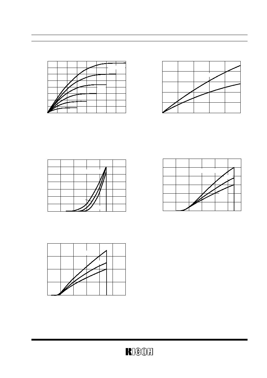
5) Nch Driver Output Current vs. Input Voltage
R
◊
5VT45C
R
◊
5VT45C
R
◊
5VT09C
R
◊
5VT27C
R
◊
5VT45C
R
◊
5VT
0
0
5
10
15
20
25
30
35
40
0.5
1.0
1.5
2.0
2.5
3.0
3.5
4.0
V
DS
(V)
O
u
t
p
u
t
C
u
r
r
e
n
t
I
O
U
T
(
m
A
)
3.5V
3.0V
2.5V
2.0V
1.5V
Topt=25∞C
V
DD
=4.0V
0
0
0.20
0.15
0.10
0.05
0.25
0.02
0.04
0.06
0.08
0.10
V
DS
(V)
O
u
t
p
u
t
C
u
r
r
e
n
t
I
O
U
T
(
m
A
)
Topt=25∞C
0.7V
V
DD
=0.8V
0
0
0.1
0.2
0.3
0.4
0.5
0.6
0.7
0.2
0.4
0.6
0.8
1.0
1.2
Input Voltage V
IN
(V)
V
DS
=0.5V
O
u
t
p
u
t
C
u
r
r
e
n
t
I
O
U
T
(
m
A
)
25∞C
Topt=80∞C
≠30∞C
V
DS
=0.5V
0
0
2
4
6
8
10
12
0.5
1.0
1.5
2.0
2.5
3.0
Input Voltage V
IN
(V)
O
u
t
p
u
t
C
u
r
r
e
n
t
I
O
U
T
(
m
A
)
25∞C
80∞C
Topt=≠30∞C
0
0
5
10
15
20
1
2
3
4
5
6
Input Voltage V
IN
(V)
V
DS
=0.5V
O
u
t
p
u
t
C
u
r
r
e
n
t
I
O
U
T
(
m
A
)
25∞C
80∞C
Topt=≠30∞C
R
◊
5VT
20
R
◊
5VT09C
6) Pch Driver Output Current vs. Input Voltage
R
◊
5VT45C
R
◊
5VT27A
R
◊
5VT09A
R
◊
5VT27C
7) Output Delay Time vs. Load Capacitance
0
2
4
6
8
0.0
0.2
0.4
0.6
0.8
1.0
1.2
1.4
Input Voltage V
IN
(V)
O
u
t
p
u
t
C
u
r
r
e
n
t
I
O
U
T
(
m
A
)
0.5V
Topt=25∞C
V
DS
=0.7V
0
1
2
3
4
5
6
7
0
0.5
1.0
1.5
2.0
2.5
3.0
Input Voltage V
IN
(V)
O
u
t
p
u
t
C
u
r
r
e
n
t
I
O
U
T
(
m
A
)
Topt=25∞C
1.5V
1.0V
0.5V
V
DS
=2.1V
0
2
4
6
8
10
0
1
2
3
4
Input Voltage V
IN
(V)
O
u
t
p
u
t
C
u
r
r
e
n
t
I
O
U
T
(
m
A
)
Topt=25∞C
1.5V
1.0V
0.5V
V
DS
=2.1V
0.0001
0.001
0.01
0.1
0.01
0.1
1
10
100
Load Capacitance C
OUT
(µF)
O
u
t
p
u
t
D
e
l
a
y
T
i
m
e
t
p
(
m
s
)
t
PHL
t
PLH
0.0001
0.001
0.01
0.1
0.01
0.1
1
10
100
Load Capacitance C
OUT
(µF)
O
u
t
p
u
t
D
e
l
a
y
T
i
m
e
t
p
(
m
s
)
t
PHL
t
PLH

21
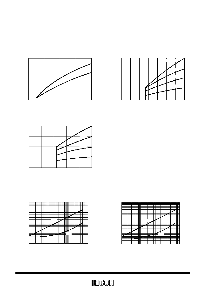
8) Output Delay Time vs. Input Pin Capacitance
R
◊
5VT45A
R
◊
5VT27A
R
◊
5VT09A
R
◊
5VT45A
R
◊
5VT
0.0001
0.001
0.01
0.1
0.01
0.1
1
10
100
Load Capacitance C
OUT
(µF)
O
u
t
p
u
t
D
e
l
a
y
T
i
m
e
t
p
(
m
s
)
t
PHL
t
PLH
0.0001
0.001
0.01
0.1
0.01
0.1
1
10
100
Input Pin Capacitance C
IN
(µF)
O
u
t
p
u
t
D
e
l
a
y
T
i
m
e
t
p
(
m
s
)
t
PHL
t
PLH
0.0001
0.001
0.01
0.1
0.01
0.1
1
10
100
Input Pin Capacitance C
IN
(µF)
O
u
t
p
u
t
D
e
l
a
y
T
i
m
e
t
p
(
m
s
)
t
PHL
t
PLH
0.0001
0.001
0.01
0.1
0.01
0.1
1
10
100
Input Pin Capacitance C
IN
(µF)
O
u
t
p
u
t
D
e
l
a
y
T
i
m
e
t
p
(
m
s
)
t
PHL
t
PLH
R
◊
5VT
22
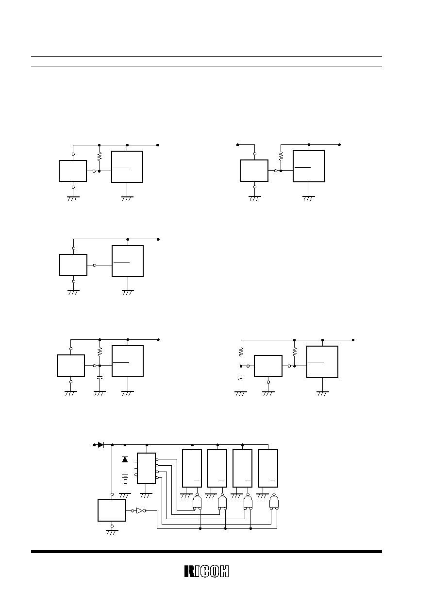
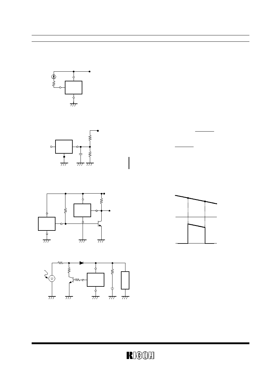
TYPICAL APPLICATIONS
∑
R
◊
5VT
◊◊
A CPU Reset Circuit (Nch Open Drain Output)
(1)Input Voltage to R
◊
5VT
◊◊
A is the same as
the input voltage to CPU.
(2) Input Voltage to R
◊
5VT
◊◊
A is different
from the input voltage to CPU.
∑
R
◊
5VT
◊◊
A Output delay Time Circuit 2
∑
Memory Back-up Circuit
∑
R
◊
5VT
◊◊
A Output delay Time Circuit 1
∑
R
◊
5VT
◊◊
C CPU Reset Circuit (CMOS Output)
R
V
DD
GND
OUT
470k
R
◊
5VT
◊◊
A
SERIES
V
DD
V
DD
CPU
RESET
GND
V
DD
V
DD1
V
DD2
GND
OUT
470k
R
R
◊
5VT
◊◊
A
SERIES
V
DD
CPU
RESET
GND
V
DD
V
DD
OUT
GND
R
◊
5VT
◊◊
C
SERIES
V
DD
CPU
RESET
GND
V
DD
V
DD
OUT
470k
R
GND
R
◊
5VT
◊◊
A
SERIES
V
DD
CPU
RESET
GND
V
DD
V
DD
GND
OUT
470k
100k
R2
R1
R
◊
5VT
◊◊
A
SERIES
V
DD
CPU
RESET
GND
OUT
D2
A
B
G
Y1
Y2
Y3
Y4
D1
V
CC
RAM1
GND CS
V
CC
RAM2
GND CS
V
CC
RAM3
GND CS
V
CC
RAM4
GND CS
GND
V
DD
V
DD
GND
V
CC
R
◊
5VT
◊◊
C
SERIES
R
◊
5VT
23
∑
Voltage Level Indicator Circuit (lighted when the power runs out)
( Nch Open Drain Output)
∑
Detector Threshold Changing Circuit
(Nch Open Drain Output)
∑
Window Comparator Circuit
(Nch Open Drain Output)
Changed Detector Threshold =
∑ (≠V
DET
)
Hysteresis Voltage =
∑ V
HYS
(Note) Please note that when the value of Ra becomes excessively large, the detector
threshold detected may differ from the value calculated by use of the above for-
mula.
Ra + Rb
Rb
Ra + Rb
Rb
V
DD
V
DD
GND
OUT
R
◊
5VT
◊◊
A
SERIES
C
V
DD
V
DD
OUT
GND
Ra
Rb
R
◊
5VT
◊◊
A
SERIES
+
V
DD
V
DD
V
DD
GND
GND
OUT
OUT
OUT
V
DET
2
V
DET
1
R
◊
5VT
◊◊
A
SERIES
R
◊
5VT
◊◊
A
SERIES
V
DD
V
DET
1
V
DET
2
VSS
OUT
VSS
∑
Excessive Charge Preventing Circuit
OUT
R2
R1
R3
R4
V
DD
V
SS
L
o
a
d
D1
S
o
l
a
r
B
a
t
t
e
r
y
Light
R
◊
5VT
◊◊
C
SERIES

R
◊
5VT
24
1. When R
◊
5VT
◊◊
C (CMOS Output) is used in FIG. 9, this IC may oscillate by the through-type current at the
detection when impedance is connected between Power Source V
DD
and R
◊
5VT V
DD
Pin.When
R
◊
5VT
◊◊
A (Nch Open Drain Output) is used in FIG. 9, and R becomes excessively large, Detector Threshold
may be varied because of the voltage drop of the supply current in the IC itself.
2. The connection as shown in FIG. 10 may cause the oscillation in both R
◊
5VT
◊◊
C (CMOS Output) and
R
◊
5VT
◊◊
A (Nch Open Drain Output).
FIG.9
SERIES
R
◊
5VT
V
DD
V
DD
GND
OUT
R2
R1
FIG.10
APPLICATION HINTS
SERIES
V
DD
V
DD
OUT
R
GND
R
◊
5VT
R
◊
5VT
25
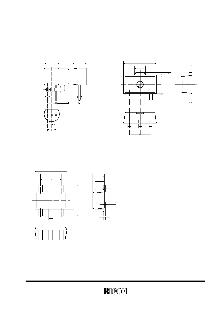
PACKAGE DIMENSIONS
(Unit: mm)
∑
TO-92
∑
SOT-89
∑
SOT-23-5
5.2MAX.
4.2MAX.
2
.
3
M
A
X
.
5
.
2
M
A
X
.
1
2
.
7
M
A
X
.
0.6MAX.
0.55MAX.
1.27
2.54
1
2
3
0
.
7
0.5MAX.
4.5±0.1
0.4±0.1
0.4±0.1
1.5±0.1
1.6±0.2
1.5±0.1
±0.1
±0.1
±0.1
1.5±0.1
2
.
5
±
0
.
1
0
.
4
M
I
N
.
4
.
2
5
M
A
X
.
0
.
8
¯1.0
1
2
3
0.42
0.4 7
0.42
2.9
±
0.2
0.4
±
0.1
1.9
±
0.2
(0.95)
(0.95)
5
4
1
2
3
+
0
.
2
≠
0
.
1
1
.
6
+0.2
≠0.1
1.1
+0.1
≠0.05
0.15
2
.
8
±
0
.
3
0 to 0.1
0
.
2
M
I
N
.
0.8
±
0.1

R
◊
5VT
26
TAPING SPECIFICATIONS
(Unit: mm)
∑
TO-92
(Note) When taping is conducted, the pins of TO-92 are
subjected to a particular forming.
(Note) TZ type tape is not in the form of a reel, but is
packed in a zigzag state in a box.Therefore, the
tape can be used as either an RF type tape or an
RR type tape,depending upon the pulling out
direction (B or F).
∑
SOT-23-5
∑
SOT-89
RF
RR
±1.0
0.3
12.7
12.7
¯ 4.0±0.2
6
.
0
±
0
.
5
±
9
.
0
±
0
.
5
0
.
5
M
A
X
.
1
8
.
0
+
1
.
0
≠
0
.
5
1
6
.
0
±
0
.
5
1
9
.
0
±
0
.
5
2
4
.
7
M
A
X
.
1.45 MAX.
0.7±0.2
*
*
: Mark Side
When TZ type tape is
pulled out from the
direction B
When TZ type tape is
pulled out from the
direction F
User Direction of Feed
(Note)
User Direction of Feed.
T 1
¯
T 2
8.0±0.1
5.0
1.5
4.0±0.1
2.0±0.05
1
.
5
±
0
.
1
5
.
6
5
±
0
.
0
5
4
.
7
1
2
±
0
.
3
+0.1
≠0
2.5MAX.
0.3±0.1
T R
T L
2.0MAX.
0.3±0.1
4.0±0.1
2.0±0.05
4.0±0.1
3.3
3.2
8
.
0
±
0
.
3
1
.
7
5
±
0
.
1
3
.
5
±
0
.
0
5
1.5
+0.1
≠0
¯
User Direction of Feed.
5.2 MAX.
4.2 MAX.
2
.
3
M
A
X
.
5
.
2
M
A
X
.
1
2
.
7
M
A
X
.
0.6 MAX.
0.55
1
2
3
0
.
7
0.5 MAX.
MAX.
2.5 ≠0.1
+0.4

RICOH COMPANY, LTD.
ELECTRONIC DEVICES DIVISION
HEADQUARTERS
13-1, Himemuro-cho, Ikeda City, Osaka 563-8501, JAPAN
Phone 81-727-53-1111 Fax 81-727-53-6011
YOKOHAMA OFFICE (International Sales)
3-2-3, Shin-Yokohama, Kohoku-ku, Yokohama City, Kanagawa 222-8530,
JAPAN
Phone 81-45-477-1697 Fax 81-45-477-1694 ∑ 1695
http://www.ricoh.co.jp/LSI/english/
RICOH CORPORATION
ELECTRONIC DEVICES DIVISION
SAN JOSE OFFICE
3001 Orchard Parkway, San Jose, CA 95134-2088, U.S.A.
Phone 1-408-432-8800 Fax 1-408-432-8375