
- 1 -
s
OUTLINE
The RS5C372B is a CMOS type real-time clock which is connected to the CPU via 2-wire and capable of serial
transmission of clock and calendar data to the CPU. The RS5C372B can generate various periodic interrupt
clock pulses lasting for long period (one month), and alarm interrupt can be made by days of the week, hours,
and minutes by two incorporated systems. Since an oscillation circuit is driven at a constant voltage, it
undergoes fluctuations of few voltage and consequently offers low current consumption (0.5µA at 3V). It also
provides an oscillator halt sensing function applicable for data validation at power-on and other occasions and
32kHz clock output (CMOS output) for an external micro computer. The product also incorporates a time
trimming circuit that adjusts the clock with higher precision by adjusting any errors in crystal oscillator
frequencies based on signals from the CPU. The crystal oscillator may be selected between 32.768kHz or
32.000kHz types. Integrated into an ultra compact and ultra thin 8 pin SSOP package, the RS5C372B is the
optimum choice for equipment requiring small sized and low power consuming products.
s
Features
q
Time keeping voltage 1.45V to 6.0V
q
Lowest supply current 0.5µA TYP (0.9µA MAX)
at 3V(25
∞
C)
(0.9µA MAX) at 3V(-40 to +85
∞
C)
q
Connected to the CPU via only 2-wire (I
2
C-bus interface, max.400KHz, address 7bits)
q
A clock counter (hours, minutes, and seconds) and a calendar counter (leap years, years, months, days,
and days of the week) in BCD codes
q
Interrupt to the CPU (period of one month to half second, with interrupt flag, interrupt halt function)
(/INTR)
q
Two systems of alarm functions (days of the week, hours, and minutes) (/INTR)
q
Oscillation halt sensing to judge internal data validity
q
Clock output of 32.768kHz(32.000kHz) ( output controllable via a register)
(32KOUT:CMOS push-pull output)
q
Second digit adjustment by ±30 seconds
q
Automatic leap year recognition up to the year 2099
q
12-hour or 24-hour time display selectable
q
Oscillation stabilizing capacity (CG, CD) incorporated
q
High precision clock error adjustment circuit
q
Oscillator of 32.768kHz or 32.000kHz may be used
q
CMOS logic
q
Package:8pin SSOP
*) I
2
C-bus is a trademark of PHILIPS ELECTRONICS N.V.
s
Block Diagram
32kHz OUTPUT
CONTROL
OSC
COMPARATOR_B
ALARM_B REGISTER
(WEEK,MIN,HOUR)
ADDRESS
DECODER
ADDRESS
REGISTER
OSC
DETECT
DIV
TIME COUNTER
(SEC,MIN,HOUR,WEEK,DAY,MONTH,YEAR)
SHIFT REGISTER
I/O
CONTROL
OSCIN
OSCOUT
INTERRUPT CONTROL
SDA
SCL
/INTR
DIVIDER
CORREC
-TION
VDD
VSS
COMPARATOR_A
ALARM_A REGISTER
(WEEK,MIN,HOUR)
32KOUT
RS5C372B
I
2
C-bus Serial Interface
Real Time Clock (8pin SSOP)
Dec. 15 '97
RS5C372B
- 2 -
s
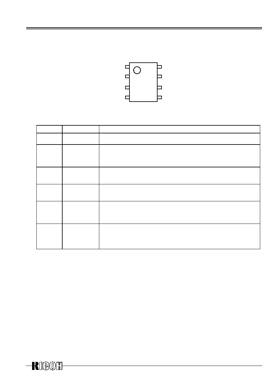
Pin Configuration
SCL
SDA
/INTR
VSS
VDD
OSCIN
OSCOUT
1
2
3
4
5
6
7
8
TOP VIEW
RS5C372B (8PIN SSOP)
32KOUT
s
Pin Description
Symbol
Pin Name
Description
SCL
Shift clock input This pin is used to input shift clock pulses to synchronize data input/output to
and from the SDA pin with this clock. Up to 6V beyond VDD may be input.
SDA
Serial input
output
This pin inputs and outputs written or read data in synchronization with shift
clock pulses from the SCL pin. Up to 6V beyond VDD may be input. This
pin functions as an Nch open drain output.
/INTR
Interrupt
output
This pin outputs periodic interrupt pulses and alarm interrupt (ALARM_A,
ALARM_B) to the CPU. This pin is off when power is activated from 0V.
This pin functions as an Nch open drain output.
32KOUT
32K Clock
Output
This pin outputs 32.768kHz pulses (when 32.768kHz crystal is used),
It outputs 32.768kHz when power source is activated from 0V. This pin
functions as an CMOS push-pull output.
OSCIN
OSCOUT
Oscillator
circuit
input/output
These pins configure an oscillator circuit by connecting a 32.768kHz or
32.000kHz crystal oscillator between the OSCIN≠OSCOUT pins.
(Any other oscillator circuit components are built into the RS5C372B.)
VDD
VSS
Positive power
supply input
Negative power
supply input
The VDD pin is connected to the positive power supply and Vss to the
ground.

RS5C372B
- 4 -
s
DC Characteristics
Unless otherwise specified: VSS=0V, VDD=3V, Topt=-40 to +85
∞
C
, Oscillation Frequency=32.768kHz or 32.000KHz(R1=30k
)
Symbol
Item
Pin Name
Conditions
MIN.
TYP.
MAX.
Unit
VIH
"H" input Voltage
SCL, SDA
0.8
VDD
6.0
V
VIL
"L" input voltage
SCL, SDA
-0.3
0.2
VDD
V
IOH
"H" output current 32KOUT
VOH=VDD-0.5V
-0.5
mA
IOL1
"L" output current /INTR, 32KOUT VOL1=0.4V
1
mA
IOL2
SDA
VOL2=0.6V
6
IILK
Input leakage
current
SCL
VI=6V or VSS
VDD=6V
-1
1
µA
IOZ
Output off state
leakage current
SDA, /INTR,
32KOUT
VO=6V or VSS
VDD=6V
-1
1
µA
IDD1 Standby current
VDD
VDD=3V, Topt=25
∞
C
0.5
0.9
µA
SCL,SDA=3V
Output=OPEN *)
IDD2
VDD
VDD=3V,
Topt=-40 to +85
∞
C
1.0
µA
SCL,SDA=3V
Output=OPEN *)
IDD3
VDD
VDD=6V
0.8
2.0
µA
SCL,SDA=6V
Output=OPEN *)
CG
Internal oscillation
capacitance 1
OSCIN
10
pF
CD
Internal oscillation
capacitance 2
OSCOUT
10
pF
*) The mode outputs no clock pulses and output is open (output off state).
For consumption current (output: no load) when 32kHz pulses are output from 32KOUT, see "Typical
Characteristics Measurement ".
RS5C372B
- 5 -
s
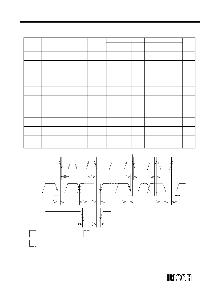
AC Characteristics
Unless otherwise specified: VSS=0V,Topt=-40 to +85
∞
C
I/O Conditions: VIH=0.8
◊
VDD,VIL=0.2
◊
VDD,VOL=0.2
◊
VDD,CL=50pF
VDD
2.0V
VDD
2.5V
Symbol
Item
Condi-
tions
MIN.
TYP.
MAX.
MIN.
TYP.
MAX.
Unit
f
SCL
SCL clock frequency
0
100
0
400
kHz
t
LOW
SCL clock "L" time
4.7
1.3
µ
s
t
HIGH
SCL clock "H" time
4.0
0.6
µ
s
t
HD;STA
Hold time for a (repeated)
start condition
4.0
0.6
µ
s
t
SU;STO
Set-up time for a stop
condition
4.0
0.6
µ
s
t
SU;STA
Set-up time for a repeated
start condition
4.7
0.6
µ
s
t
SU;DAT
Data set-up time
250
100
ns
t
HDH;DAT
"H" Data hold time
0
0
ns
t
HDL;DAT
"L" Data hold time
35
35
ns
t
PL;DAT
SDA low stable time after
falling of SCL
2.0
0.9
µ
s
t
PZ;DAT
SDA off stable time after
falling of SCL
2.0
0.9
µ
s
t
R
Rising time of SCL and
SDA (input)
1000
300
ns
t
F
Falling time of SCL and
SDA (input)
300
300
ns
t
SP
Pulse width of spikes which
must be suppressed by the
input Filter
50
50
ns
SDA(OUT)
SCL
S
Sr
P
t
PZ;DAT
t
HIGH
t
SU;DAT
t
HDH;DAT
t
HD;STA
t
SP
t
SU;STO
t
LOW
t
SU;STA
SDA(IN)
t
HD;STA
t
PL;DAT
Sr
P
Stop Condition
S
Start Condition
Repeated Start condition
t
HDL;DAT
*For detailed information refer to "
s
Operation 1.2. I
2
C-BUS
transmission system"
