 | –≠–Ľ–Ķ–ļ—ā—Ä–ĺ–Ĺ–Ĺ—č–Ļ –ļ–ĺ–ľ–Ņ–ĺ–Ĺ–Ķ–Ĺ—ā: RS5C62 | –°–ļ–į—á–į—ā—Ć:  PDF PDF  ZIP ZIP |

REAL-TIME CLOCK
RP/ RF/ RS5C62
ELECTRONIC DEVICES DIVISION
NO.EA-012-9803
APPLICATION MANUAL

NOTICE
1. The products and the product specifications described in this application manual are subject to change or dis-
continuation of production without notice for reasons such as improvement. Therefore, before deciding to use
the products, please refer to Ricoh sales representatives for the latest information thereon.
2. This application manual may not be copied or otherwise reproduced in whole or in part without prior written con-
sent of Ricoh.
3. Please be sure to take any necessary formalities under relevant laws or regulations before exporting or other-
wise taking out of your country the products or the technical information described herein.
4. The technical information described in this application manual shows typical characteristics of and example
application circuits for the products. The release of such information is not to be construed as a warranty of or a
grant of license under Ricoh's or any third party's intellectual property rights or any other rights.
5. The products listed in this document are intended and designed for use as general electronic components in
standard applications (office equipment, computer equipment, measuring instruments, consumer electronic
products, amusement equipment etc.). Those customers intending to use a product in an application requiring
extreme quality and reliability, for example, in a highly specific application where the failure or misoperation of
the product could result in human injury or death (aircraft, spacevehicle, nuclear reactor control system, traffic
control system, automotive and transportation equipment, combustion equipment, safety devices, life support
system etc.) should first contact us.
6. We are making our continuous effort to improve the quality and reliability of our products, but semiconductor
products are likely to fail with certain probability. In order prevent any injury to persons or damages to property
resulting from such failure, customers should be careful enough to incorporate safety measures in their design,
such as redundancy feature, fire-containment feature and fail-safe feature. We do not assume any liability or
responsibility for any loss or damage arising from misuse or inappropriate use of the products.
7. Anti-radiation design is not implemented in the products described in this application manual.
8. Please contact Ricoh sales representatives should you have any questions or comments concerning the prod-
ucts or the technical information.
June 1995

OUTLINE
......................................................................................................
1
FEATURES
....................................................................................................
1
BLOCK DIAGRAM
.........................................................................................
1
PIN CONFIGURATION
...................................................................................
2
PIN DESCRIPTION
........................................................................................
2
ABSOLUTE MAXIMUM RATINGS
...................................................................
3
RECOMMENDED OPERATING CONDITION
....................................................
3
DC ELECTRICAL CHARACTERISTICS
...........................................................
4
AC ELECTRICAL CHARACTERISTICS
...........................................................
5
TIMING CHART
.............................................................................................
5
FUNCTIONAL DESCRIPTION
.........................................................................
6
1. Addressing
.................................................................................................
6
2. Functions of Registers
...................................................................................
7
3. Functions of Counters
..................................................................................
15
USAGE
........................................................................................................
17
1. Reading and Writing Operations
......................................................................
17
2. Handling of CE Pin
......................................................................................
18
3. Configuration of Oscillatory Circuit
....................................................................
19
4. Adjustment of Oscillation Frequencies
...............................................................
20
5. Interrupts
.................................................................................................
22
6. Timer
......................................................................................................
23
7. Detection of Stop of Oscillation
........................................................................
24
8. Typical Power Supply Circuit
...........................................................................
25
9. Typical Connection between RP/RF/RS5C62 and CPU
...........................................
26
10. Typical Characteristics
..................................................................................
27
11. Typical Software-controlled Processes
...............................................................
29
RP/RF/RS5C62
APPLICATION MANUAL
CONTENTS

QUESTIONS AND ANSWERS ON USE
.........................................................
34
PACKAGE DIMENSIONS
..............................................................................
42
TAPING SPECIFICATIONS
...........................................................................
43
REAL-TIME CLOCK
1
RP/RF/RS5C62
OUTLINE
The RP/RF/RS5C62 are CMOS LSIs which serve microcomputers as real-time clocks providing time, calendar,
and alarm functions in direct coupling with the data buses of CPUs such as 8086 and 68000. A built-in timer counter
acts as a watchdog timer or interrupt timer. They are available in three different types of packages: the DIP type,
the SOP type, and the SSOP type.
∑ Directly connected to CPU, enabling fast access.
∑ 4bit bidirectional data bus, and 4bit address bus.
∑ The oscillator is driven by a constant voltage, so the oscillation frequency is stable even when the power supply
voltage fluctuates.
∑ Built-in timer counter using internal clock.
∑ Generates cyclic CPU interrupts, and generates alarm-match interrupts.
∑ Interrupt flag and interrupt inhibit.
∑ Clock (hour, minute, second), calendar (leap year, year, month, day, day-of-the-week), alarm (hour, minute).
∑ 12-or 24-hour mode is selectable.
∑ Recognizes leap years automatically.
∑ All clock and alarm data expressed in BCD codes.
∑ Ī30 seconds adjustment function.
∑ Determines whether clock data is valid or invalid.
∑ Consumes very low power due to CMOS technology, so it can be backed up by batteries.
∑ Power supply voltage between 3.0 to 5.0V.
∑ Time keeping supply voltage between 2.0 to 6.0V.
∑ Package : 18pin DIP for RP5C62, 18pin SOP for RF5C62, 20pin SSOP for RS5C62.
FEATURES
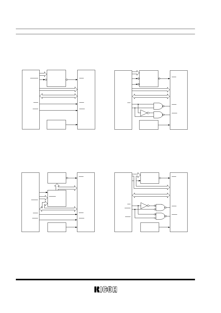
BLOCK DIAGRAM
INTERRURT
CONTROL
TIMER
CONTROL REGISTER
ADDRESS BUS
CONTROL
DATA BUS
CONTROL
D0D1D2
DIV
OSC DETECT
OSC
OSCIN
OSCOUT
CE
D3
A0 A1 A2 A3
ADDRESS
DECODER
ALARM REGISTER
COMPARATOR
WATCH & CALENDAR
VDD
VSS
TMOUT
CS
RD
WR
INTR

Function
CS and CE are used when interfacing external devices. They may be accessed
when CS is low and CE is high. CE is connected to an output of power down
detector on the system power supply side, and CS is connected to the microcom-
puter address bus.
Timer output may be used as an interrupt free-run timer or watchdog timer.
When CE is low (running on battery backup), operation stops (there is no output).
It is N-ch open drain output.
Address input is connected to the CPU address bus. It is gated internally with CE.
When RD falls from high to low, the contents of the counters or registers specified
by A0 to A3 are output to D0 to D3. It is valid when CS is low and CE is high. It is
CMOS input.
When WR falls from high to low or rises from low to high, the contents of D0 to
D3 are written to registers or counters specified by A0 to A3. WR is valid when CS
is low and CE is high. It is CMOS input.
D0 to D3 are connected to the CPU data bus. The input section is gated internally
with CE. It is CMOS input/output.
INTR outputs cyclic interrupts or alarm interrupts to CPU. It also operates when
CE is low (at battery backup). It is N-ch open drain output.
Crystal oscillator of 32.768kHz must be connected between OSCIN and OSCOUT.
Capacitance is connected externally between V
DD
and OSCIN and V
DD
and
OSCOUT, forming the oscillator circuit.
V
DD
connects to +5V or +3V and V
SS
to ground.
2
PIN CONFIGURATION
RP/RF/RS5C62
VDD
VDD
OSCOUT
OSCOUT
OSCIN
OSCIN
D3
D2
D1
D0
INTR
WR
CS
CE
TMOUT
A1
A2
A3
RD
A0
VSS
1
2
3
5
6
7
8
4
9
18
17
16
14
13
12
11
15
10
INTR
D3
D2
D1
D0
WR
CE
A0
A1
A2
A3
VSS
18
17
16
15
14
13
12
11
10
1
2
3
4
5
6
7
8
9
CS
TMOUT
RD
VDD
OSCOUT
OSCIN
NC
INTR
D3
D2
D1
D0
WR
CS
CE
TMOUT
NC
A0
A1
A2
A3
RD
VSS
20
19
18
17
16
15
14
13
12
11
1
2
3
4
5
6
7
8
9
10
PIN DESCRIPTION
Pin No. Symbol
Name
1
CS
Chip select input
2
CE
Chip enable input
3
TMOUT
Timer output
4 ≠7
A0 ≠A3
Address input
8
RD
Read control input
10
WR
Write control input
11≠14
D0 ≠D3
Bi-directional data
bus
15
INTR
Interrupt output
16
OSCIN
Oscillator circuit
17
OSCOUT
input/output
18
V
DD
9
V
SS
Power supply
*
) The pin numbers marked in the above table indicate the pins on the 18pin packages.
∑ RP5C62 (18pin DIP)
∑ RF5C62 (18pin SOP)
∑ RS5C62 (20pin SSOP)
3
RP/RF/RS5C62
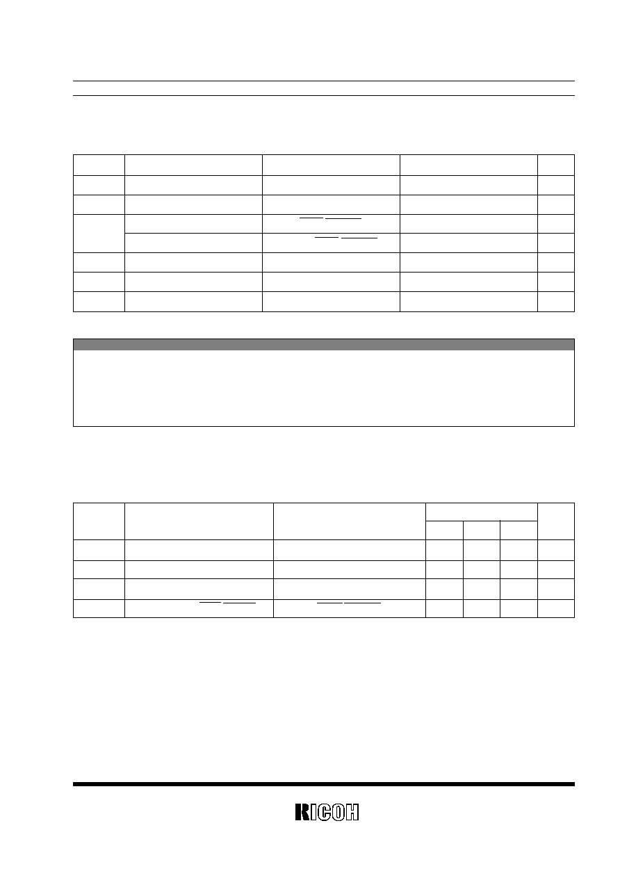
ABSOLUTE MAXIMUM RATINGS
RECOMMENDED OPERATING CONDITION
ABSOLUTE MAXIMUM RATINGS
V
SS
=0V
Symbol
Item
Conditions
Ratings
Unit
V
DD
Supply Voltage
≠0.3 to +7.0
V
V
I
Input Voltage
≠0.3 to +V
DD
+0.3
V
V
O
Output Voltage 1
INTR, TMOUT
≠0.3 to +12.0
V
Output Voltage 2
Except INTR, TMOUT
≠0.3 to +V
DD
+0.3
V
P
D
Maximum Power Dissipation
TA=25įC
300
mW
Topt
Operating Temperature
≠20 to +70
įC
Tstg
Storage Temperature
≠40 to +125
įC
V
SS
=0V, Topt=≠20 to +70įC
Symbol
Item
Conditions
Limits
Unit
MIN.
TYP.
MAX.
V
DD
Supply Voltage
2.7
5.0
6.0
V
V
CLK
Time Keeping Supply voltage
2.0
6.0
V
f
XT
Crystal Oscillation Frequency
32.768
kHz
V
PUP
Pull-up Voltage for INTR, TMOUT pin
INTR, TMOUT
10
V
Absolute Maximum ratings are threshold limit values that must not be exceeded even for an instant under
any conditions. Moreover, such values for any two items must not be reached simultaneously. Operation
above these absolute maximum ratings may cause degradation or permanent damage to the device. These
are stress ratings only and do not necessarily imply functional operation below these limits.
4
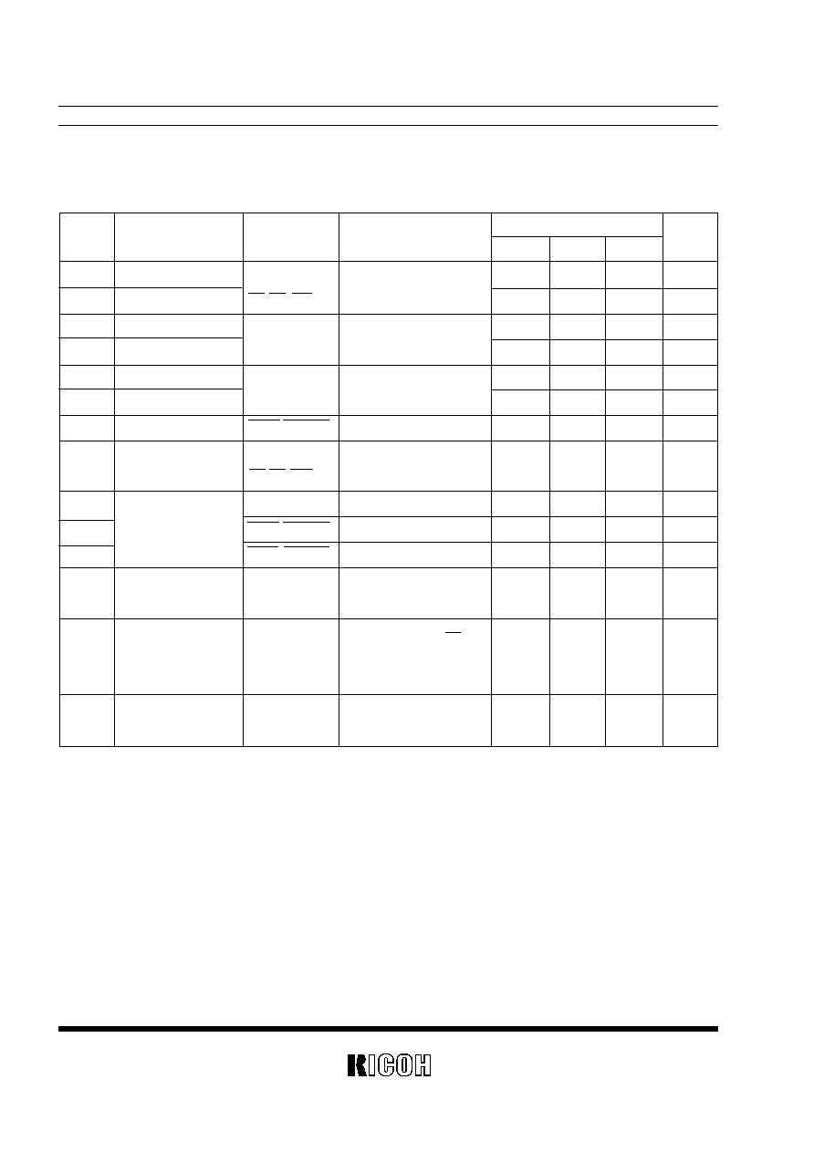
DC ELECTRICAL CHARACTERISTICS
RP/RF/RS5C62
Unless Noted, V
SS
=0V, V
DD
=5VĪ10%, Topt=≠20 to +70įC, X'tal=32.768kHz, (R
1
≤35kĹ), C
G
=10pF, C
D
=10pF
Symbol
Item
Pin Name
Conditions
Limits
Unit
MIN.
TYP.
MAX.
V
IH1
"H" input voltage
A0 to A3, D0 to D3
2.2
V
DD
+0.3
V
V
IL1
"L" input voltage
CS, RD, WR
≠0.3
0.8
V
V
IH2
"H" input voltage
CE
0.8
īV
DD
V
DD
+0.3
V
V
IL2
"L" input voltage
≠0.3
0.2
īV
DD
V
V
OH1
"H" output voltage
D0 to D3
I
OH1
=≠400ĶA
2.4
V
V
OL1
"L" output voltage
I
OL1
=2mA
0.4
V
V
OL2
"L" output voltage
INTR, TMOUT
I
OL2
=2mA
0.4
V
I
ILK
Input leak current
A0 to A3, CE,
V
ILK
=V
DD
or V
SS
≠1
1
ĶA
CS, RD, WR
I
OZ1
Output off leak
D0 to D3
V
OZ1
=V
DD
or V
SS
≠5
5
ĶA
I
OZ2
current
INTR, TMOUT
V
OZ2
=V
DD
≠2
2
ĶA
I
OZ3
INTR, TMOUT
V
OZ3
=10V
≠5
5
ĶA
I
DD1
Consumption
V
DD
V
DD
=2.5V, CE=L
3
ĶA
current for back-up
Others : OPEN
Consumption
V
DD
=5.5V, CE=H, CS=H,
I
DD2
current for stand-by
V
DD
Output : OPEN
8
ĶA
Input : V
DD
or V
SS
∂f
Oscillation frequency
OSCIN
V
DD
=2.5 to 5.5V
≠1
1
ppm
drift for voltage drift
OSCOUT
Topt=25įC
5
RP/RF/RS5C62
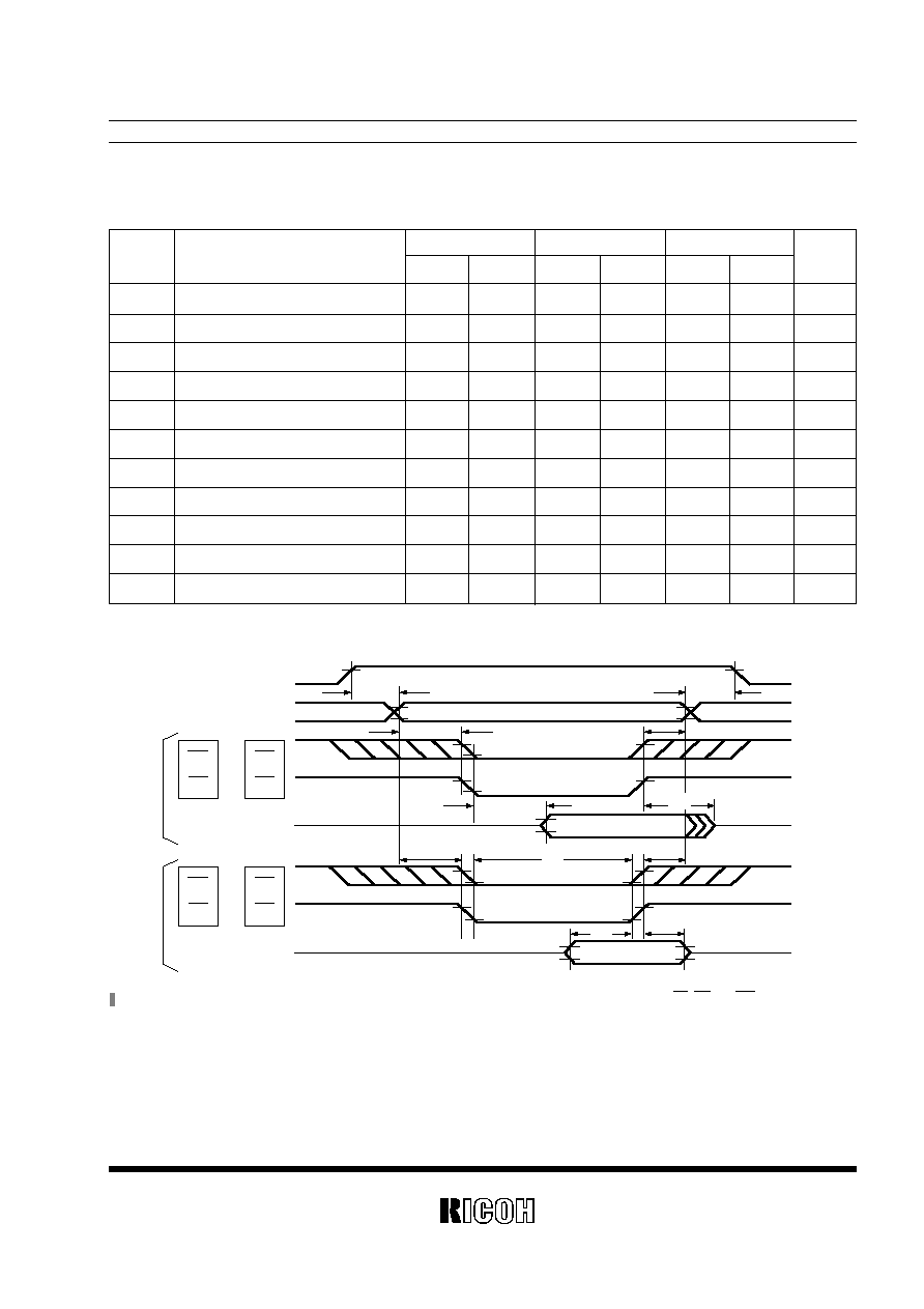
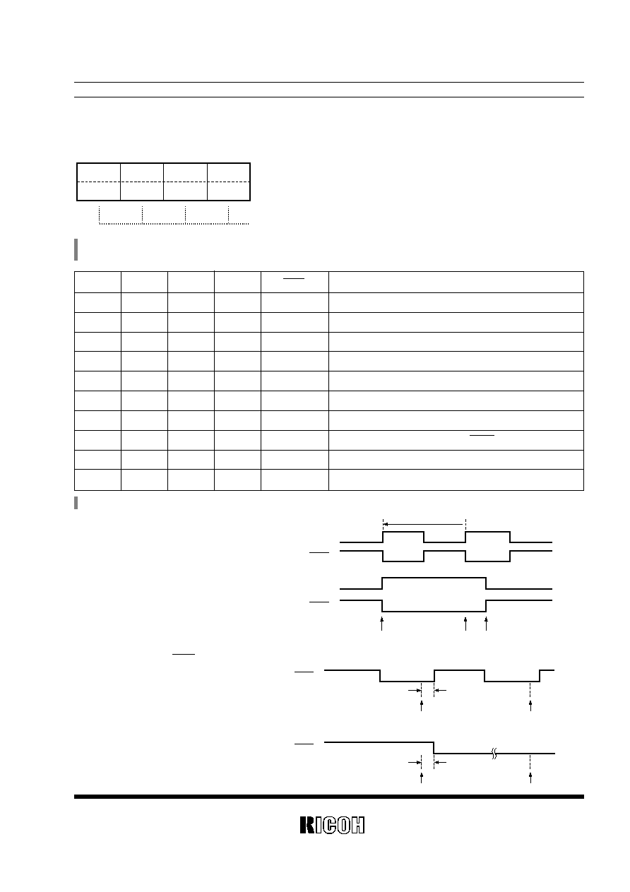
AC ELECTRICAL CHARACTERISTICS
TIMING CHART
V
SS
=0V, Topt=≠20 to +70įC
Symbol
Item
V
DD
=5VĪ10%
V
DD
=3VĪ10%
V
DD
=5VĪ20%
Unit
MIN.
MAX.
MIN.
MAX.
MIN.
MAX.
t
CES
CE Setup Time
500
1,000
500
ns
t
CEH
CE Hold Time
500
1,000
500
ns
t
AS
(RD)
Address Setup Time (For Read)
20
20
20
ns
t
AS
(WR)
Address Setup Time (For Write)
20
20
20
ns
t
AH
(RD)
Address Hold Time (For Read)
10
10
10
ns
t
AH
(WR)
Address Hold Time (For Write)
10
10
10
ns
t
RR
Output Data Delay Time (C
L
=100pF)
120
295
150
ns
t
RZ
Output Data Floating Time
70
95
75
ns
t
W
Write Pulse Width
120
195
150
ns
t
DS
Input Data Setup Time
60
95
75
ns
t
DH
Input Data Hold Time
10
10
10
ns
Read
CE
or
or
A0 to A3
D0 to D3
(Read Data)
D0 to D3
(Write Data)
Write
CS
RD
RD
CS
CS
WR
WR
CS
t
CES
t
CEH
t
DH
Valid
Valid
t
RR
t
AH(RD)
t
AS(RD)
t
AS(WR)
t
AH(WR)
t
RZ
t
DS
t
W
*
) The diagonally shaded sections marked in the above timing chart indicate the allowable high or low levels of the CS, RD, and WR pin inputs.
Input/Output Conditions
(V
DD
= 5VĪ10%)
(V
DD
= 3VĪ10%)
(V
DD
= 5VĪ20%)
V
IH
= 2.2V
V
IH
= 0.8
ī
V
DD
V
IH
= 2.4V
V
IL
= 0.8V
V
IL
= 0.2
ī
V
DD
V
IL
= 0.4V
V
OH
= 2.2V
V
OH
= 0.8
ī
V
DD
V
OH
= 2.4V
V
OL
= 0.8V
V
OL
= 0.2
ī
V
DD
V
OL
= 0.4V
6
RP/RF/RS5C62
FUNCTIONAL DESCRIPTION
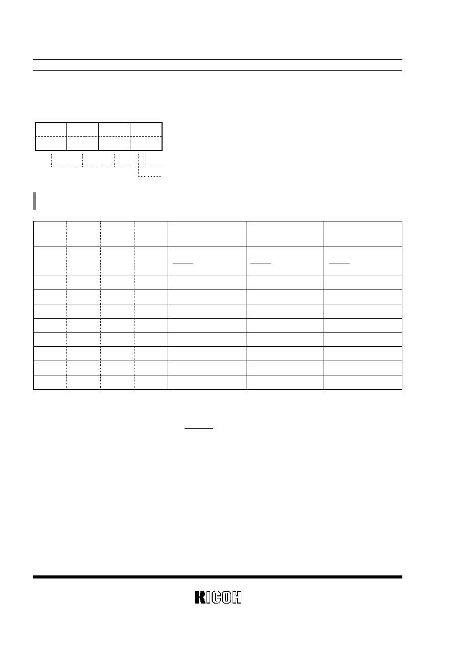
1. Addressing
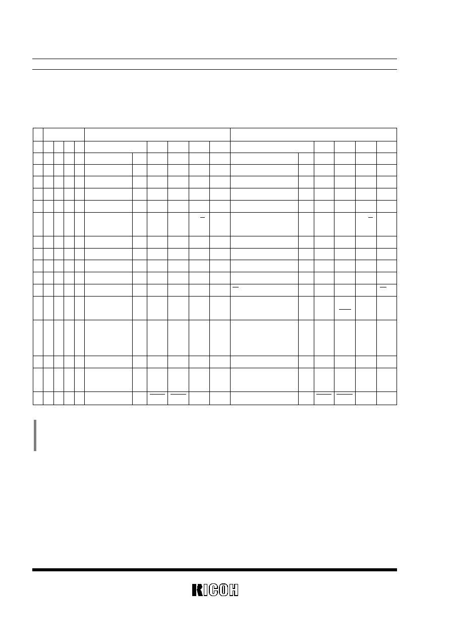
Address Bus
BANK 0 (BANK=0)
BANK 1 (BANK=1)
A3 A2 A1 A0
Description
D3
D2
D1
D0
Description
D3
D2
D1
D0
0
0
0
0
0
1 sec. Counter
R/W
S
8
S
4
S
2
S
1
Cyclic interrupt select Reg. W/O
CT
3
CT
2
CT
1
CT
0
1
0
0
0
1
10 sec. Counter
R/W
S
40
S
20
S
10
Adust Reg.
W/O
ADJ
2
0
0
1
0
1 min. Counter
R/W
M
8
M
4
M
2
M
1
1 min. alarm Reg.
R/W
AM
8
AM
4
AM
2
AM
1
3
0
0
1
1
10 min. Counter
R/W
M
40
M
20
M
10
10 min. alarm Reg.
R/W
AM
40
AM
20
AM
10
4
0
1
0
0
1 hour Counter
R/W
H
8
H
4
H
2
H
1
1 hour alarm Reg.
R/W
AH
8
AH
4
AH
2
AH
1
5
0
1
0
1
10 hour Counter
R/W
P/A
H
10
10 hour alarm Reg.
R/W
AP/A
AH
10
or H
20
or AH
20
6
0
1
1
0
day-of-the-week Counter R/W
W
4
W
2
W
1
7
0
1
1
1
1 day Counter
R/W
D
8
D
4
D
2
D
1
8
1
0
0
0
10 day Counter
R/W
D
20
D
10
9
1
0
0
1
1 month Counter R/W
MO
8
MO
4
MO
2
MO
1
A
1
0
1
0
10 month Counter R/W
MO
10
12/24 select Reg.
W/O
12/24
B
1
0
1
1
1 year Counter
R/W
Y
8
Y
4
Y
2
Y
1
Leap Year Reg.
R/O
LY
1
LY
0
R/W
LYE
W/O
TM
2
TM
1
TM
0
C
1
1
0
0
10 year Counter
R/W
Y
80
Y
40
Y
20
Y
10
Timer Clock Select Reg.
R/W
TM
3
R/O
TMFG
D
1
1
0
1
Control Reg. 1
W/O WTEN ALEN
TMR
BANK Control Reg. 1
W/O WTEN ALEN
TMR
BANK
E
1
1
1
0
Control Reg. 2
R/O
BSY
Control Reg. 2
R/O
BSY
R/W
CTFG
ALFG
XSTP
R/W
CTFG
ALFG
XSTP
F
1
1
1
1
Control Reg. 3
W/O TSTA
TSTB WTRST
Control Reg. 3
W/O TSTA
TSTB WTRST
*
1) R/W bits can be read and written. R/O bits can only be read. W/O bits can only be written.
*
2) It is no problem to attempt writing to R/O bits and blank bits, but the attempt will fail.
*
3) If W/O bits and blank bits are read, the returned value is 0.
*
4) The control registers 1, 2, and 3 have the same address assignment for BANK0 and BANK1.
7
RP/RF/RS5C62
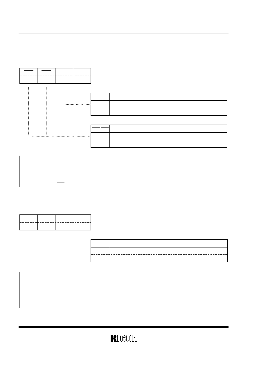
2. Functions of Registers
2.1 Control Register 1 (Bank0/1 at "Dh")
D3
D2
D1
D0
0
0
0
0
WTEN
ALEN
TMR
BANK
(For write operation)
(For read operation)
*
1
Bank switching bit
BANK
Function
0
1
Specifies selection of BANK0 in the address table.
Specifies selection of BANK1 in the address table.
TMR
Function
0
1
Specifies no change.
Specifies resetting of the timer conditional on restart.
Timer resetting bit *
2
ALEN
Function
0
1
Disables an alarm interrupt.
Enables an alarm interrupt.
Alarm operation setting bit *
3
WTEN
Function
0
1
Disables a carry to the 1-second time digit.
Enables a carry to the 1-second time digit.
Time count operation setting bit *
4
*
1) The BANK bit is intended for only write operation and always read as "0".
*
2) The timer frequency can be set by the timer clock selection register.
*
3) Setting the ALEN bit to "0" during output of an alarm interrupt from the INTR pin (while it is held low) turns off the INTR pin.
Setting the ALEN bit to "1" in matching between clock time and alarm time drives the INTR pin low within a maximum of 61.1Ķs.
*
4) A 1-second carry with the WTEN bit set to "0" increments the second digit by 1 upon setting of the WTEN bit to "1". This bit will
automatically be set to "1" upon driving low the CE pin.
8
RP/RF/RS5C62
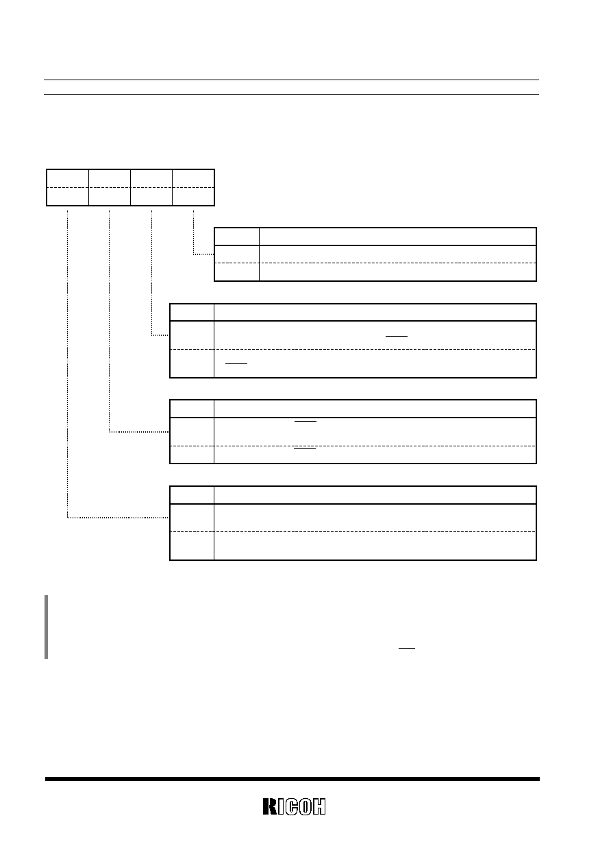
2.2 Control Register 2 (BANK0/1 at "Eh")
D3
D2
D1
D0
BSY
CTFG
ALFG
XSTP
CTFG
ALFG
XSTP
(For write operation)
(For read operation)
XSTP
Function
0
1
Indicates the progress of oscillation. Intended for setting to "0".
Indicates the stop of oscillation. Not intended for setting to "1".
ALFG
Function
0
1
Indicates an alarm interrupt is disabled or indicates mismatching between clock
time and alarm time (upon turning off the INTR pin). Intended for setting to "0".
I
ndicates matching between clock time and alarm time (upon driving low the
INTR pin). Not intended for setting to "0".
Alarm time match indication bit *
3
CTFG
Function
0
1
Indicates that the INTR pin is turned off. Intended for setting to "0" in the level
mode.
Indicates that the INTR pin is driven low. Not intended for setting to "0".
Cyclic interrupt indication bit *
4
BSY
Function
0
1
Indicates the normal state of the time and calendar counters (no carry or no
reset pulse).
Indicates the busy state of the time and calendar counters (a carry or a reset
pulse generated).
Time/calendar counter state indication bit *
5
*
*
1
Oscillation stop detection bit *
2
*
1) The BSY bit is intended for only read operation and is not intended for write operation.
*
2) The XSTP bit is used to detect the stop of the crystal oscillator. The XSTP bit is set to "1" upon the stop of oscillation and held at "1" after the restart
of oscillation. Upon detection of the stop of oscillation, the built-in timer counter is reset (because the TM
3
bit in the timer clock selection register is
reset).
*
3) When the ALEN bit is set to "1", the ALFG bit is also set to "1" upon output of an alarm interrupt from the INTR pin (while it is held low).
9
RP/RF/RS5C62
*
4) The CTFG bit is set to "1" upon output of a cyclic interrupt from the INTR pin (while it is held low).
(A cyclic interrupt may occur in the pulse mode and the level mode.)
ALFG
INTR
Alarm time match
Alarm time match
Setting the ALFG
bit to "0"
Alarm time match
CTFG
INTR
CTFG
INTR
Interrupt
Preset interrupt cycle
Setting the CTFG bit to "0"
Interrupt
*
5) When the BSY bit is set to "1", write operation must not be performed upon the time and calendar counters which are being updated. Normally, read
operation must be performed from the counters upon setting the BSY bit to "0". Reading from them without checking the BSY bit requires separate
software for preventing reading errors. The BSY bit is set to "1" in the four cases below:
Setting the ADJ bit to "1"
Setting the WTEN bit to "1"
Setting the WTRST bit to "1"
Completion of reset
Completion of pulse for carry to second digit
Completion of correction by +1
Completion of adjustment
MAX.122.1Ķs
MAX.122.1Ķs
MAX.122.1Ķs
30.5Ķs
91.6Ķs
∑ Pulse mode
(The CT
3
bit is set to "0".)
(The CTFG bit is not intended for write
operation.)
∑ Level mode
(The CT
3
bit is set to "1".)
(The CTFG bit is intended for setting to "0"
only.)
(I) Adjustment by Ī30 seconds
(II) Correction by +1
(when there is a 1-second carry in transition of the
WTEN bit from "0" to "1")
(III) Normal 1-second carry
(IV) Counter resetting (setting of WTRST bit)
(Resetting the 1 to 8Hz dividers)
10
RP/RF/RS5C62
2.3 Control Register 3 (BANK0/1 at "Fh")
D3
D2
D1
D0
0
0
0
0
(For write operation)
(For read operation)
*
2
Bit for resetting lower-order counter than the second counter. *
3
WTRST
Function
0
1
Specifies normal operation.
Specifies resetting of 1- to 8-Hz dividers conditional on restart.
TSTA,TSTB
Function
0
1
Specifies setting of the test mode.
Specifies setting of normal operation.
Test mode setting bits *
4
TSTA
TSTB
WTRST
*
*
1
*
1) The bit marked with "
*
" is not intended for write operation.
*
2) This bit is intended for only write operation and always read as "0".
*
3) When set to "1", the WTRST bit specifies resetting of the lower-order counter than the 1 second counter ranging from 8Hz and 4Hz to 2Hz and 1Hz
conditional on restart. The WTRST bit is used to adjust the lower-order counter than the 1 second counter. After the WTRST bit is set to "1", the
BSY bit is set to "1" for a maximum of 122.1Ķs.
*
4) Both the TSTA and TSTB bits must be set to "1" to specify normal operation and will automatically be set to "1" upon driving low the CE pin.
2.4 Adjustment Register (BANK1 at "1h")
D3
D2
D1
D0
0
0
0
0
(For write operation)
(For read operation)
*
2
Second digit adjustment bit *
3
Function
0
1
Specifies normal operation.
Specifies adjustment of second digit.
*
*
1
*
*
ADJ
ADJ
*
1) The bits marked with "
*
" are not intended for write operation.
*
2) This bit is intended for only write operation and always read as "0".
*
3) The ADJ bit is used to correct the second digit. When set to "1", the ADJ bit functions as follows:
1) For digits ranging from 00 seconds to 29 seconds
ģ
Resets the lower-order counter than the 1 second counter (in the same manner as the
WTRST bit) and sets the second digit to "00".
2) For digits ranging from 30 seconds to 59 seconds
ģ
Resets the second and lower-order counters (in the same manner as the WTRST bit), sets
the second digit to "00" and increments the minute digit by 1. The BSY bit is set to "1" for a maximum of 122.1Ķs after the ADJ bit is set to "1".
11
RP/RF/RS5C62
2.5 Interrupt Cycle Selection Register (BANK1 at "0h")
D3
D2
D1
D0
0
0
0
0
CT
3
CT
2
CT
1
CT
0
(For write operation)
(For read operation)
*
1
Interrupt cycle/output mode selection bits *
2
*
1) These bits are intended for only write operation and always read as "0".
*
2) The CT
3
to CT
0
bits are used to set interrupt cycles and output modes as shown in the table below:
*
) The bits marked with "
*
" are set to "0" or "1".
CTFG
Preset interrupt cycle
INTR
CTFG
INTR
Interrupt
Setting the CTFG bit to "0"
(Interrupt)
∑ Pulse mode
(The CT
3
bit is set to "0".)
(The CTFG bit is not intended for write operation.)
∑ Level mode
(The CT
3
bit is set to "1".)
(The CTFG bit is intended for setting to "0" only.)
CT3
CT2
CT1
CT0
INTR
Remarks
*
0
0
0
"OFF"
Disable a cyclic interrupt.
*
0
0
1
2048Hz
Specify a cycle (T) of 0.488ms (1/2048Hz).
*
0
1
0
1024Hz
Specify a cycle (T) of 0.977ms (1/1024Hz).
*
0
1
1
128Hz
Specify a cycle (T) of 7.813ms (1/128Hz).
*
1
0
0
16Hz
Specify a cycle (T) of 62.5ms (1/16Hz).
*
1
0
1
1Hz
Specify a cycle (T) of 1s (1/1Hz).
*
1
1
0
1/60Hz
Specify a cycle (T) of 60s (1/1/60Hz).
*
1
1
1
"ON"
Specify the fixed low level of the INTR pin output.
0
*
*
*
Pulse mode
Specify a duty cycle of 50%. See below.
1
*
*
*
Level mode
See below.
∑ Relationship between INTR pin output and
upward second count
INTR
INTR
Upward second count
Upward second count
Upward second count
Upward second count
(1) Pulse mode (when 1Hz or 1/60Hz is selected)
(2) Level mode (when 1Hz or 1/60Hz is selected)
30.5Ķs
30.5Ķs
D3
D2
D1
D0
AM
8
AM
4
AM
2
AM
1
(For read and write operations) 1-minute alarm digit (at "2h")
*
AM
40
AM
20
AM
10
(For read and write operations) 10-minute alarm digit (at "3h")
AH
8
AH
4
AH
2
AH
1
(For read and write operations) 1-hour alarm digit (at "4h")
*
*
AP/A or AH
20
AH
10
(For read and write operations) 10-hour alarm digit (at "5h")
12
RP/RF/RS5C62
2.6 Alarm Register (1-minute, 10-minute, 1-hour, and 10-hour) (BANK1 at "2h to 5h")
*
1) The bits marked with "
*
" are always read as "0" and not intended for write operation.
*
2) When enabling an alarm interrupt, non-existent minute and hour alarm digits must not be left (to prevent mismatching between clock time and alarm
time).
*
3) Alarm minute and hour settings are exemplified in the table below:
*
4) In the the 12-hour time scale, the hour digits of 12 and 32 indicate 0 o'clock a.m. and 0 o'clock p.m., respectively.
Alarm minute
12-hour time scale
24-hour time scale
and hour setting
10-hour
1-hour
10-minute 1-minute
10-hour
1-hour
10-minute 1-minute
digit
digit
digit
digit
digit
digit
digit
digit
0 : 00 a.m.
1
2
0
0
0
0
0
0
1 : 30 a.m.
0
1
3
0
0
1
3
0
11 : 59 a.m.
1
1
5
9
1
1
5
9
0 : 00 p.m.
3
2
0
0
1
2
0
0
1 : 30 p.m.
2
1
3
0
1
3
3
0
11 : 59 p.m.
3
1
5
9
2
3
5
9
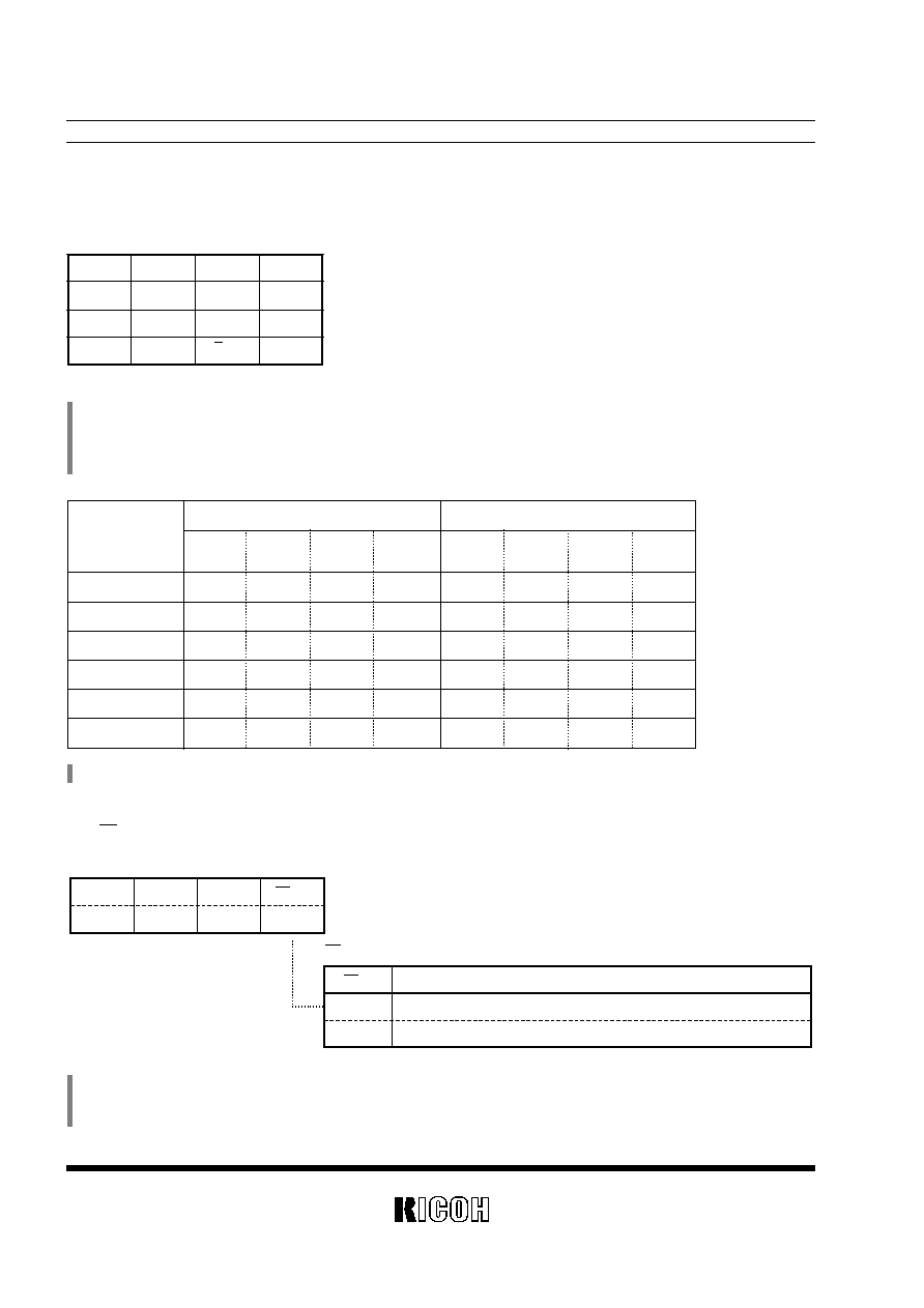
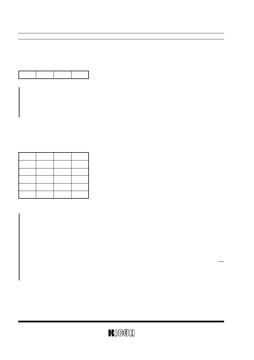
2.7 12/24-hour Time Scale Selection Register (BANK1 at "Ah")
D3
D2
D1
D0
0
0
0
0
(For write operation)
(For read operation)
*
2
12/24-hour time scale selection bit *
3,4
Function
0
1
Selects the 12-hour time scale with a.m. and p.m. indications.
Selects the 24-hour time scale.
*
*
1
*
*
12/24
12/24
*
1) The bits marked with "
*
" are not intended for write operation.
*
2) These bits are intended for only write operation and always read as "0".
*
3) The time digits are indicated in binary-coded decimal (BCD) notation as shown in the table below:
13
RP/RF/RS5C62
*
4) The 12-hour or 24-hour time scale must be selected before time of day adjustment or alarm time setting
(e.g. at the time of initialization after power-on from 0V)
D3
D2
D1
D0
0
LY
1
LY
0
(For write operation)
(For read operation)
(LY
1
,LY
0
)
Function
(0,0)
Any other value
Specifies leap year indication (including February 29) (when
the LYE bit is set to "0".
Specifies normal year indication (not including February 29).
*
*
1
*
*
Leap year indication bits (intended for only read operation) *
2
Function
0
1
Enables leap year indication.
Disables leap year indication.
Leap year indication selection bit *
3,4
LYE
LYE
LYE
2.8 Leap Year Indication Register (BANK1 at "Bh")
24-hour time scale 12-hour time scale 12-hour time scale 24-hour time scale
00
12 (AM12)
12
32 (PM12)
01
01 (AM 1)
13
21 (PM 1)
02
02 (AM 2)
14
22 (PM 2)
03
03 (AM 3)
15
23 (PM 3)
04
04 (AM 4)
16
24 (PM 4)
05
05 (AM 5)
17
25 (PM 5)
06
06 (AM 6)
18
26 (PM 6)
07
07 (AM 7)
19
27 (PM 7)
08
08 (AM 8)
20
28 (PM 8)
09
09 (AM 9)
21
29 (PM 9)
10
10 (AM10)
22
30 (PM10)
11
11 (AM11)
23
31 (PM11)
*
1) The bits marked with "
*
" are not intended for write operation.
*
2) The LY1 and LY0 bits cycle from "00" via "01" and "10" to "11" with the passage of years.
*
3) Upon setting the LYE bit to "0", automatic correction is made for leap years in the years 1901 to 2099 (e.g. 1992, 1996, and 2000).
Upon setting the LYE bit to "1", leap year indication is disabled (counting up to February 28).
*
4) Writing to the 1-year or 10-year counter enables leap year indication (sets the LYE bit to "0").
14
RP/RF/RS5C62
*
1) Only the TM
3
bit is intended for read operation. The D0 bit is always read as "TMFG". The D2 and D1 bits are always read as "0".
*
2) The TM
3
to TM
0
bits are used to set cycles for the counters as shown in the table below.
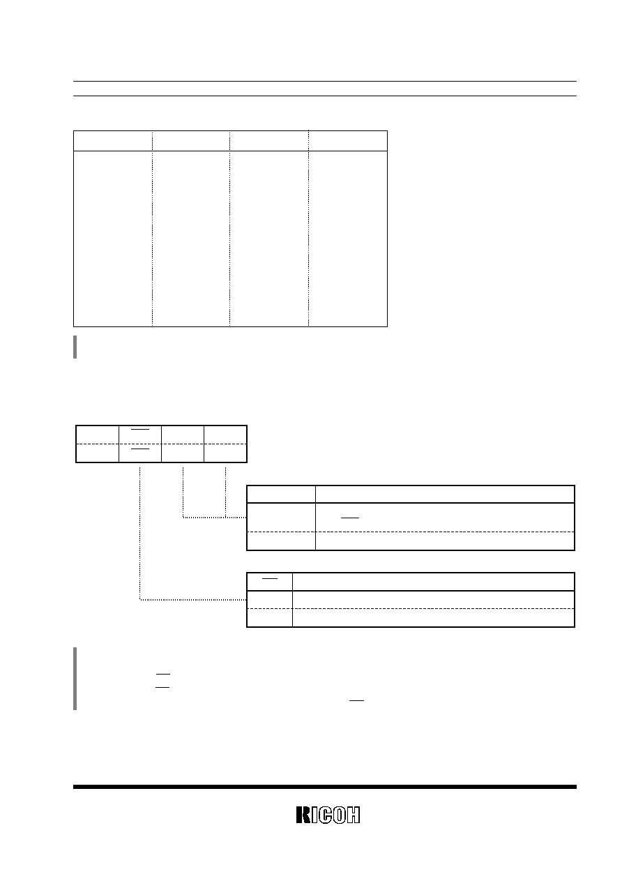
2.9 Timer Clock Selection Register (BANK1 at "Ch")
D3
D2
D1
D0
0
0
TMFG
TM
3
TM
3
TM
2
TM
1
TM
0
(For write operation)
(For read operation)
*
1
Timer counter cycle setting bit (TM
3
to TM
0
) *
2
Timer output indication bit (TMFG) *
3
T1 : Maximum time during which timer output is disabled after timer resetting.
(Timer reset occurs upon setting the TMR bit to "1" in the control register 1.)
(Timer output occurs upon driving low the TMOUT pin output.)
T2 : Time between timer output and cycle setting during timer resetting (upon setting the TM
3
bit to "0" ),
or timer resetting, or transition of the CE pin input from its low to high levels.
T3 : Timer output cycle without timer reset.
TM
3
TM
2
TM
1
TM
0
T1
T2
T3
(Watchdog timer cycle)
(Output time after timer resetting) (Free-running timer cycle)
0
*
*
*
Timer output disabled
Timer output disabled
Timer output disabled
(TMOUT pin output turned off)
(TMOUT pin output turned off)
(TMOUT pin output turned off)
1
0
0
0
562ms
562 to 626ms
625ms
1
0
0
1
281ms
281 to 313ms
312.5ms
1
0
1
0
140ms
140 to 157ms
156.3ms
1
0
1
1
70.3ms
70.3 to 78.2ms
78.13ms
1
1
0
0
35.1ms
35.1 to 39.1ms
39.06ms
1
1
0
1
17.5ms
17.5 to 19.6ms
19.53ms
1
1
1
0
8.78ms
8.78 to 9.77ms
9.766ms
1
1
1
1
4.39ms
4.39 to 4.89ms
4.883ms
D3
D2
D1
D0
S
8
S
4
S
2
S
1
(For read and write operations) 1-second time digit (at "0h")
*
S
40
S
20
S
10
(For read and write operations) 10-second time digit (at "1h")
M
8
M
4
M
2
M
1
(For read and write operations) 1-minute time digit (at "2h")
*
M
40
M
20
M
10
(For read and write operations) 10-minute time digit (at "3h")
H
8
H
4
H
2
H
1
(For read and write operations) 1-hour time digit (at "4h")
*
*
P/A or H
20
H
10
(For read and write operations) 10-hour time digit (at "5h")
15
RP/RF/RS5C62
*
3) Relationship between TMFG Bit and TMOUT pin output
*
4) The timer is stopped (the TMOUT pin output is turned off) upon driving low the CE pin input, but restarted upon driving high the CE pin input.
*
5) Timer output is disabled (the TMOUT pin output is turned off) upon resetting the TM
3
bit to "0" when the stop of oscillation is detected (setting the
XSTP bit to "1").
*
6) Timer output is turned off (the TMOUT pin output is turned off) upon setting the TMR bit to "1" in the control register 1 during timer output (while the
TMOUT pin is held low).
*
1) The bits marked with "
*
" are always read as "0" and not intended for write operation.
*
2) Upon setting the WTEN bit to "0" in the control register 1, a carry to the 1-second time digit from the second counter is disabled.
*
3) The time digits are indicated in BCD notation as shown below:
Second digit: Ranges from 00 to 59 and carried to the minute digit in transition from 59 to 00.
Minute digit: Ranges from 00 to 59 and carried to the hour digit in transition from 59 to 00.
Hour digit: Ranges as shown in "2. 7 12/24-hour Time Scale Selection Register" and carried to the day or day-of-the-week digit in transition from 11
p.m. to 12 a.m. or from 23 to 00.
*
4) A carry from any non-existent time digit must be avoided because it may cause malfunction in the time counter.
TMOUT
TMFG
Setting the TMR bit to "1"
Setting the TMR bit to "1"
0.244ms
MAX.T
1
T
2
T
3
3. Functions of Counters
3.1 Time Counter (BANK0 at "0h to 5h")
D3
D2
D1
D0
D
8
D
4
D
2
D
1
(For read and write operations) 1-day calendar digit (at "7h")
*
*
1
*
D
20
D
10
(For read and write operations) 10-day calendar digit (at "8h")
MO
8
MO
4
MO
2
MO
1
(For read and write operations) 1-month calendar digit (at "9h")
*
*
*
MO
10
(For read and write operations) 10-month calendar digit (at "Ah")
Y
8
Y
4
Y
2
Y
1
(For read and write operations) 1-year calendar digit (at "Bh")
Y
80
Y
40
Y
20
Y
10
(For read and write operations) 10-year calendar digit (at "Ch")
D3
D2
D1
D0
*
W
4
W
2
W
1
(For read and write operations) Day-of-the-week counter
16
RP/RF/RS5C62
*
1) The bits marked with "
*
" are always read as "0" and not intended for write operation.
*
2) The day-of-the-week counter is incremented by 1 in a carry to the 1-day calendar digit.
*
3) Days of the week written to the W
4
, W
2
, and W
1
bits are counted up in septimal notation as shown below :
(000)
ģ
(001)
ģ
.....
ģ
(110)
ģ
(000)
The correspondence between days of the week and readings of the day-of-the-week counter is user-definable (e.g. Sunday=000)
*
4) The W
4
, W
2
, and W
1
bits must not be all set to 1.
3.2 Day-of-the-week Counter (BANK0 at "6h")
3.3 Calendar Counter (BANK0 at "7h" to "Ch")
*
1) The bits marked with "
*
" are always read as "0" and not intended for write operation.
*
2) The calendar digits are indicated in BCD notation by the automatic calendar function as shown below:
Day digit
: Ranges from 1 to 31 (in January, March, May, July, August, October, and December)
Ranges from 1 to 30 (in April, June, September, and November)
Ranges from 1 to 29 (in February in leap years)
Ranges from 1 to 28 (in February in normal years)
Carried to the month digit in transition back to 1.
Month digit : Ranges from 1 to 12 carried to the year digit in transition back to 1.
Year digit : Ranges from 00 to 99 including leap years of 00, 04, 08, - - - - - -, 92, and 96 (when leap year indication is enabled by setting the LYE
bit in the leap year indication register to "0" ).
*
3) A carry from any non-existent calendar digit must be avoided because it may cause malfunction in the calendar counter.
17
RP/RF/RS5C62
USAGE
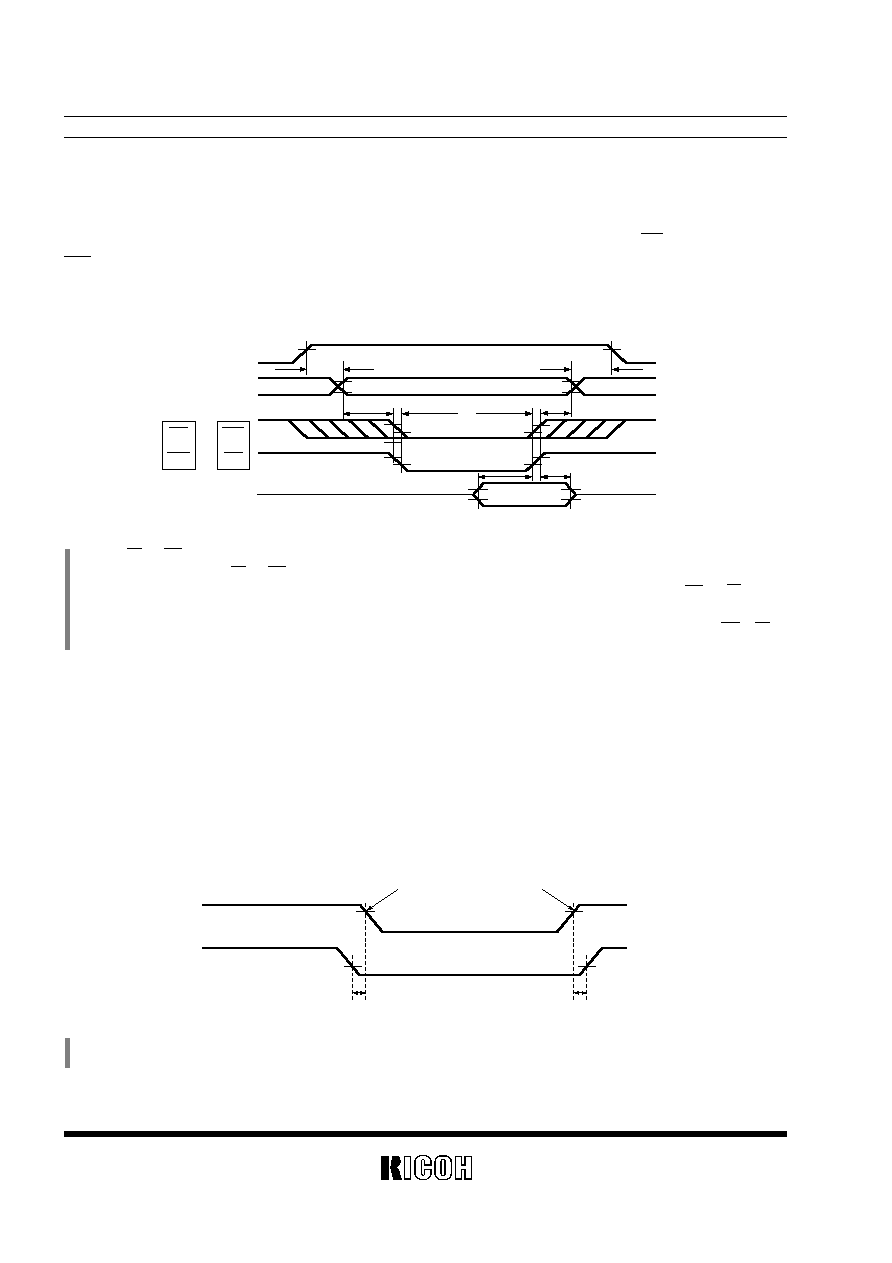
1. Reading and Writing Operations
CE
Address
Reading operation
Writing operation
Data bus
A3 to A0
D3 to D0
CS
WR
RD
Upon driving high the CE pin, the interfacing input/out-
put pins are enabled, establishing equivalence in logic
between the RD and CS pin inputs during read opera-
tion and between the WR and CS pin inputs during
write operation. Upon driving low the CE pin, the inter-
facing input/output pins are disabled, preventing occur-
rence of invalid leak current due to their floating. The
CE pin must always be driven either high or low and
must never be left floating.
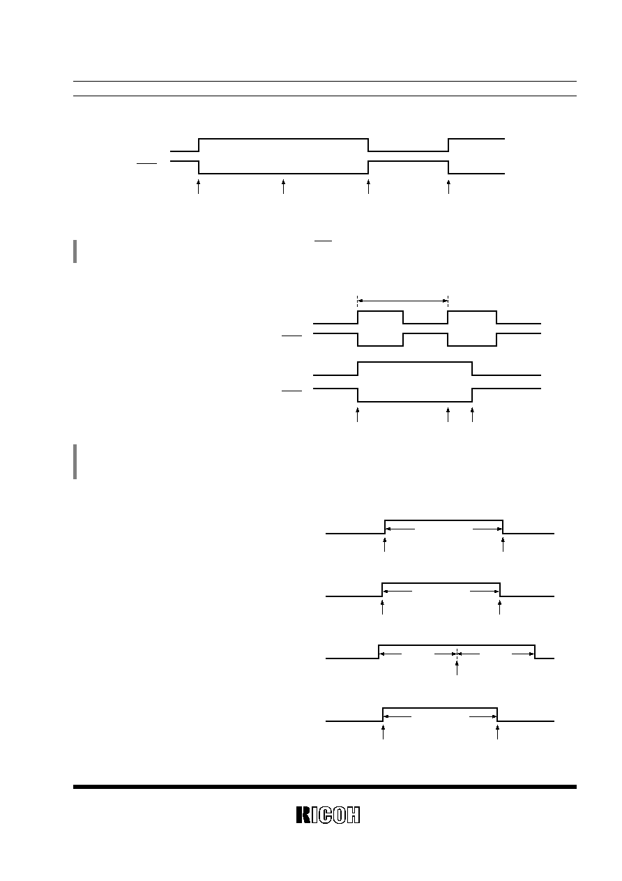
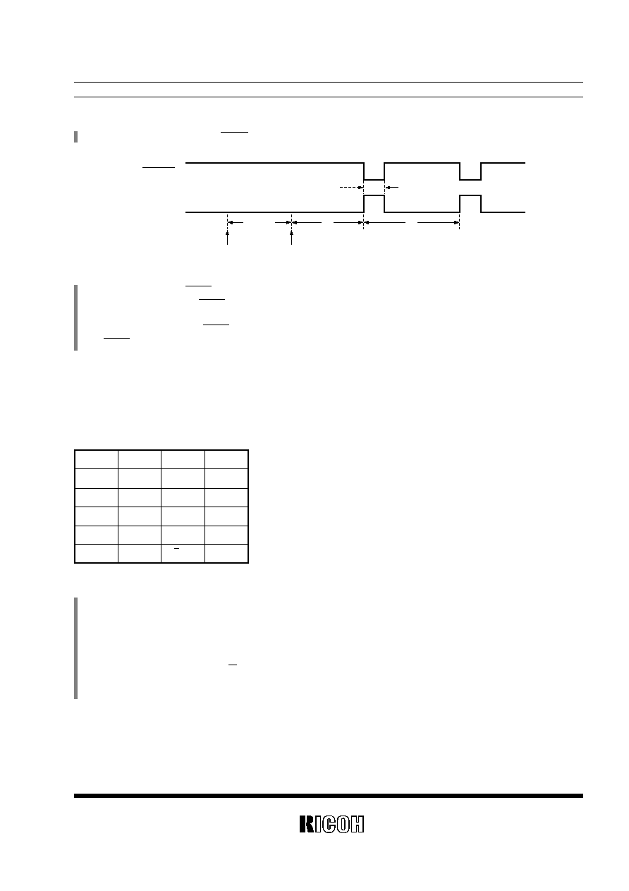
1.1 Reading Operation
The requirements for reading data from the internal registers and counters are: [1] holding the CE pin high, [2]
performing the process of addressing through the A3 to A0 pin inputs, then [3] driving low the CS pin, [4] causing
the RD pin to transition from its high to low levels, and thereby [5] causing the D3 to D0 pins to output read data.
The reading timing is shown in the chart below.
CE
A0 to A3
D0 to D3
(Read Data)
t
CEH
t
CES
Valid
t
AH(RD)
t
AS(RD)
t
RZ
t
RR
or
CS
RD
RD
CS
[1]
[2]
[3]
[4]
[5]
*
1) The CS and RD pin inputs are interchangeable. The diagonally shaded sections marked in the above timing chart may be set to both high and low
levels. (Consequently, the CS and RD pin inputs may be caused to transition from their high to low levels before the process of addressing.)
*
2) "
t
AS
(RD)" indicates the time required to perform the process of addressing before the start of read operation at which both the RD and CS pin inputs
are driven low.
*
3) "
t
AH
(RD)"indicates the time required to maintain the result of addressing after the completion of read operation at which either the RD or CS pin input
is driven high.
18
RP/RF/RS5C62
1.2 Writing Operation
The requirements for writing data to the internal registers and counters are: [1] holding the CE pin high, [2] per-
forming the process of addressing through the A3 to A0 pin inputs, then [3] driving low the CS pin, [4] causing the
WR pin to transition from its high to low to high levels, and thereby [5] causing the D3 to D0 pins to input data to be
written. The writing timing is shown in the chart below.
CE
A0 to A3
D0 to D3
(Write Data)
t
CEH
t
CES
Valid
t
AH(WR)
t
AS(WR)
t
DH
t
DS
or
CS
WR
WR
CS
t
W
[1]
[2]
[3]
[4]
[5]
*
1) The CS and WR pin inputs are interchangeable. The diagonally shaded sections marked in the above timing chart may be set to both high and low
levels. (Consequently, the CS and WR pin inputs may be caused to transition from their high to low levels before the process of addressing.)
*
2) "
t
AS
(WR)" indicates the time required to perform the process of addressing before the start of write operation at which both the WR and CS pin inputs
are driven low.
*
3) "
t
AH
(WR)" indicates the time required to maintain the result of addressing after the completion of write operation at which either the WR or CS pin
input is driven high.
*
) The CE pin must be driven as low as the V
SS
pin whenever possible in order to minimize battery consumption in battery backup (while the CE pin is
held low).
2. Handling of CE Pin
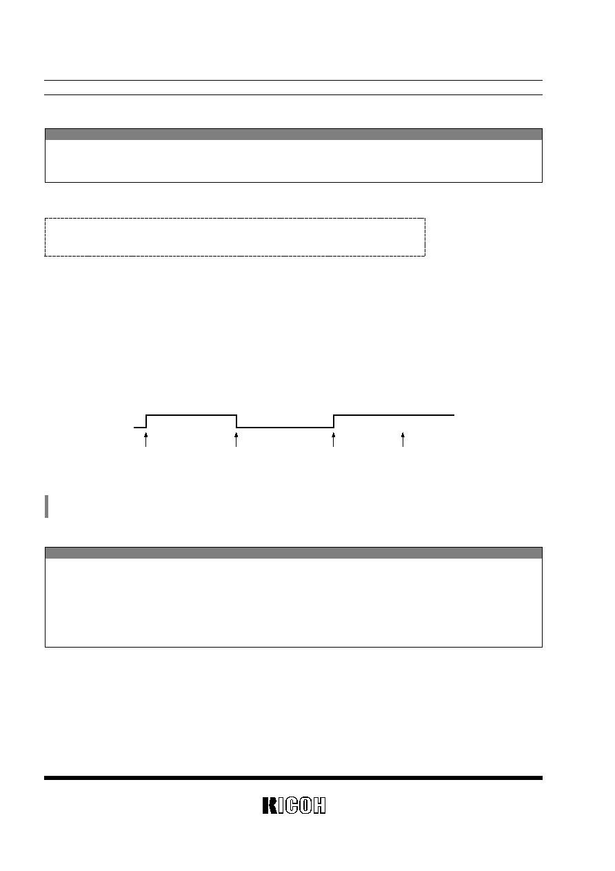
Normally, the CE pin is connected to the supply voltage detection circuit of the system power supply. In switch-
ing the system power supply (see the typical power supply circuit), the CE pin must be driven low before the voltage
across the system power supply drops below the lower limit to the operating voltage of the CPU (at the point ( [1] )
in the timing chart below) and then driven high after the supply voltage rises above the lower limit to the operating
voltage of the CPU (at the point ( [2] ) in the timing chart below).
CE
VDD
Lower limit to operating voltage of CPU
Battery voltage
0.2VDD
0.2VDD
MIN.0Ķs
MIN.0Ķs
Voltage across system
power supply
[1]
[2]
19
RP/RF/RS5C62
3. Configuration of Oscillatory Circuit
VDD
VDD
OSCOUT
OSCIN
C
G
32kHz
C
D
RP/RF/RS5C62
R
F
R
D
A
Typical external components:
X'tal : 32.768 kHz
R
1
≤
35k
Ĺ
C
G
=5pF to 35pF
C
D
=5pF to 35pF
Standard values of internal elements:
R
F
=12M
Ĺ
R
D
=60k
Ĺ
In the oscillatory circuit, which is driven by a constant voltage of about 2V relative to the VDD pin, either one end
of the oscillatory capacitors C
G
and C
D
must be connected to the VDD pin without exception.
Reference
< Considerations in Installing Components Surrounding Oscillatory Circuit >
< Other Relevant Considerations >
When either one end of the oscillatory capacitors C
G
and C
D
is connected to the VSS pin instead of the VDD
pin, the oscillatory circuit is still operational but subject directly to fluctuations in the voltage of the system
power supply. Under sharp fluctuations between 5V and battery voltage in particular, the oscillatory circuit
may be brought to a temporary stop. Thus, it is not recommendable to connect either one end of the oscilla-
tory capacitors C
G
and C
D
to the VSS pin.
1) Install the oscillatory capacitors C
G
and C
D
in the closest possible proximity to the IC.
2) Avoid laying any signal or power line in the proximity of the oscillatory circuit (particularly in the area
marked with "
¨Aģ" in the above figure).
3) Apply the highest possible insulation resistance between the OSCIN or OSCOUT pin and the printed cir-
cuit board (PCB).
4) Avoid using any long parallel line to wire the OSCIN and OSCOUT pin.
5) Take extreme care not to cause condensation, which leads to various problems such as failure of the crys-
tal oscillators.
1) When applying an external input of clock pulses (32.768kHz) to the OSCIN pin:
DC coupling ...........Prohibited due to mismatching input levels.
AC coupling ...........Permissible except that unpredictable results may occur upon detection of the stop of
oscillation if any error occurs in such detection due to such factors as noises. Timer operation is prohibit-
ed upon detection of the stop of oscillation.
2) Avoid using the oscillator output of the RP/RF/RS5C62 (from the OSCOUT pin) to drive any other IC for
the purpose of ensuring stable oscillation characteristics.
20
RP/RF/RS5C62
4. Adjustment of Oscillation Frequencies
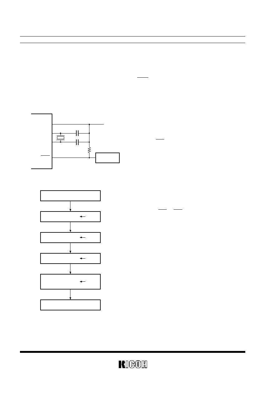
4.1 Measurement of Oscillation Frequency
The oscillation frequency can be measured by using the INTR pin output (a cyclic interrupt). Note that its mea-
surement is affected by and cannot therefore be obtained with accuracy by the OSCIN pin input and the OSCOUT
pin output, which are directly measured by such means as a probe.
Frequency
counter
V
DD
V
DD
*
3
*
2
*
1
OSCOUT
OSCIN
C
D
C
G
INTR
*
1) Use a frequency counter with 6 or more readout digits in order to ensure
an accuracy on the order of Ī1ppm.
*
2) Pull up the INTR pin to the V
DD
and set the CE pin to high.
*
3) Connect either one end of the oscillatory capacitors C
G
and C
D
to the V
DD
pin.
Power-on from 0V
*
4
*
5
*
6
*
7
*
8
Interrupt cycle
selection register
Read frequency counter
Control register 3
Ch
Control register 1
1h
Control register 2
0h
5h
*
4) Set both the TSTA and TSTB bits to "1" in the control register 3 to disable
the test circuit.
*
5) Set the ALEN bit to "0" and the BANK bit to "1" in the control register 1 to
disable an alarm interrupt.
*
6) Set both the CTFG and ALFG bits to "0" in the control register 2 to disable
an alarm interrupt and a cyclic interrupt.
*
7) Set a cyclic interrupt to 1Hz (or any other cycle) in the pulse mode.
*
8) An error of Ī1ppm for every 1Hz amounts to a time lag of approximately
2.6 seconds per month.
[Example of monthly time lag calculation given an error of Ī1ppm for
every 1Hz.
Ī1ppm x 60 seconds x 60 minutes x 24 hours x 30 days = 2.592
= approx. 2.6 seconds per month ]
21
RP/RF/RS5C62
4.2 Adjustment of Oscillation Frequencies
Select crystal oscillators
Select C
G
and C
D
*
1
*
3
YES
YES
NO
NO
*
3
*
2
*
4
END
Fix C
G
and C
D
< Unless adjustment needs to be made
to oscillation frequencies: >
< If adjustment needs to be made to
oscillation frequencies: >
Replace C
G
with trimmer capacitor
Optimize C
G
and C
D
END
Optimize C
D
Change ranking of oscillation
frequencies
Change ranking of oscillation
frequencies
Fix trimmer capacitor
Make fine adjustment to oscillation
frequencies
*
1) In selecting crystal oscillators, inquire of their suppliers. Check how the selected crystal oscillators match the RP/RF/RS 5C62 and determine the
ranking of oscillation frequencies (load capacitance (C
L
) in general and equivalent series resistance (R1).)
*
2) The oscillatory capacitor C
D
can be replaced with a trimmer capacitor to adjust oscillation frequencies.
*
3) Optimize the oscillatory capacitors C
G
and C
D
to adjust oscillation frequencies to desired values (on the actual PCB in consideration of possible influ-
ences by floating capacitance). Note that the greater capacitance of the oscillatory capacitors C
G
and C
D
tend to result in increased current con-
sumption and prolonged oscillation start time. As a guide, their recommendable capacitance ranges from 5 pF to 20 pF (10 pF to 10-odd pF in par-
ticular). (See the typical characteristic measurement.)
*
4) Set the rotational angle of the trimmer capacitor slightly below the central value in its adjustment range (to ensure matching between the central val-
ues of the rotational angle and oscillation frequencies in consideration of the fact that smaller capacitance lead to greater frequency variations).
Oscillation frequencies are subject to variations due to possible fluctuations in ambient temperature and supply
voltage (see "Typical Characteristics").
Reference
A 32kHz crystal oscillator causes a clock delay above or below the central temperature range of 20įC to 25įC.
It is therefore recommended to adjust or set oscillation frequencies in such a manner as to become slightly
high in room temperature.
22
RP/RF/RS5C62
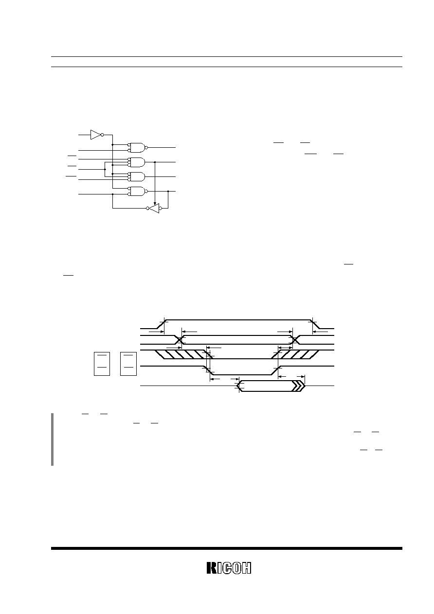
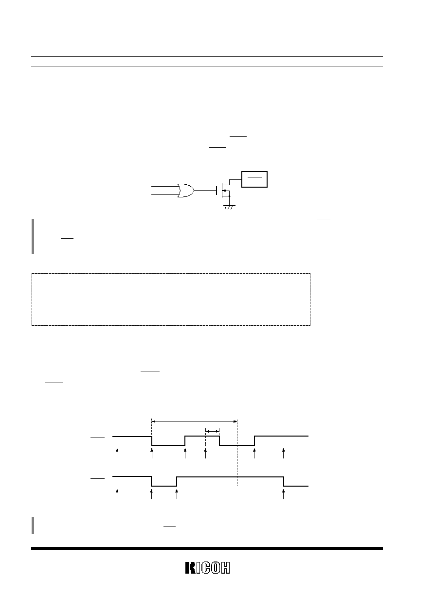
5. Interrupts
Interrupts are available in the following two types:
1) Alarm interrupt: Requested upon driving low (turning on) the INTR pin in matching between preset alarm time
(in minutes and hours) and time indicated by the time counter (in minutes and hours).
2) Cyclic interrupt: Requested upon driving low (turning on) the INTR pin with a preset cycle.
To output an alarm interrupt and a cyclic interrupt, the INTR pin is configured as shown in the figure below:
*
1) When an alarm interrupt and a cyclic interrupt are generated in combination, their logical sum (OR) is output from the INTR pin. In this event, they
can be distinguished from each other by reading the ALFG and CTFG bits of the control register 2.
*
2) The INTR pin output has indefinite states at power-on from 0V.
*
3) An alarm interrupt and a cyclic interrupt are both enabled whether the CE pin input is held high or low.
*
1) The above figure assumes that an alarm interrupt occurs in the absence of a cyclic interrupt.
*
2) The ALFG bit has an inverse logic from that of the INTR pin output.
INTR
Alarm interrupt
Cyclic interrupt
5.1 Alarm Interrupt
Desired alarm time (in minutes and hours) can be preset in the alarm digits of the alarm register with the ALEN
bit set to "0" and then to "1" in the control register 1. Upon matching between the preset alarm time and the time
indicated by the time counter, the INTR pin is driven low (turned on) to output a request for an alarm interrupt.
The INTR pin output can be controlled by using the ALEN bit in the control register 1 and the ALFG bit in the con-
trol register 2.
ALEN=1
ALEN=1
ALEN=0
ALFG=0
ALEN=1
ALEN=0
Alarm time match
Alarm time match
Alarm time match
Alarm time match
INTR
MAX.61.1Ķs
INTR
Alarm time match period: 1 minute
Alarm-time................Alarm register
(See "2. 6 Alarm Register".)
ALEN bi
(See "2. 1 Control Register 1".)
ALFG bit
(See "2. 2 Control Register 2".)
Cyclic .......................Cyclic interrupt select register
(See "2. 5 Control Register 2".)
CTFG bit
(See "2. 2 Control Register 2".)
Interrupt Registers
23
RP/RF/RS5C62
Interrupt cycle selection register
(See "2.5 Interrupt Cycle Selection Register")
CTFG bit
(See "2.2 Control Register 2")
5.2 Cyclic Interrupt
A desired interrupt cycle can be preset in the bits in the interrupt cycle selection register. With the preset inter-
rupt cycle, the INTR pin is driven low (turned on) to output an request for a cyclic interrupt. A cyclic interrupt can
be output from the INTR pin in the pulse mode and the level mode. In the level mode in particular, a cyclic interrupt
can be disabled by setting the CTFG bit to "0" in the control register 2.
Available interrupt cycles: 6 types (0.488ms, 0.977ms, 7.813ms, 62.5ms, 1s, and 60s)
Available output modes: 2 types (pulse mode and level mode)
CTFG
Preset interrupt cycle
INTR
CTFG
INTR
Interrupt
Setting the CTFG bit to "0"
(Interrupt)
*
1) A preset interrupt cycle can be canceled by setting the bits to "0" in the interrupt cycle selection register.
*
2) The above figure assumes that a cyclic interrupt occurs in the absence of an alarm interrupt.
*
3) The CTFG bit has an inverse logic from that of the INTR pin output.
*
1) The timer is stopped upon driving low the CE pin input, but restarted upon driving high the CE pin input.
*
2) Timer output is disabled upon resetting the TM
3
bit to "0" when the stop of oscillation is detected.
*
3) The T3 to T1 bits are described in "2. 9 Timer Clock Selection Register".
*
4) Timer output is turned off upon setting the TMR bit to "1" in the control register 1 during timer output.
Cyclic Interrupt
6. Timer
Upon lapse of time preset in the timer clock selection register, cyclic pulses are output from the TMOUT pin.
The timer counter can be reset conditional on restart by setting the TMR bit to "1" in the control register 1. (It can
act as a watchdog timer.)
TMOUT
TMFG
Setting the TMR bit to "1"
Setting the TMR bit to "1"
0.244ms
MAX.T
1
T
2
T
3
∑ Pulse mode
(The CT
3
bit is set to "0".)
(The CTFG bit is not intended for write
operation.)
∑ Level mode
(The CT
3
bit is set to "1".)
(The CTFG bit is intended for setting to
"0" only.)
24
RP/RF/RS5C62
Timer clock selection register and TMFG bit
(See "2.9 Timer Clock Selection Register")
TMR bit
(See "2.1 Control Register 1")
Elements Involved in Timer
Reference
Considerations in Using XSTP Bit
7. Detection of Stop of Oscillation
The stop of oscillation can be detected by monitoring the XSTP bit in the control register 2. Namely, the XSTP
bit is switched from "0" to "1" upon detection of the stop of oscillation. This principle can be used to check the valid-
ity of time data.
(The stop of oscillation can also be detected by using the software-controlled processes described in 11.1.2
Initialization Subject to Setting of XSTP Bit. "Initialization at Power-on".)
Power-on from 0V
*
1
XSTP
Stop of oscillation
Setting the XSTP bit to "0"
(During oscillation)
Restart of oscillation
*
2
*
1) The XSTP bit is set to "1" at power-on from 0V. Note that the XSTP bit may be locked at instantaneous power disconnection.
*
2) Once the stop of oscillation has been detected, the XSTP bit is kept at "1" even after the restart of oscillation.
It is recommended to update the settings of the timer clock selection register at regular time intervals to
improve the stability of timer operation.
Ensure error-free detection of the stop of oscillation by:
1) Preventing the VDD pin input from making instantaneous power disconnection.
2) Preventing the crystal oscillators causing condensation.
3) Preventing the crystal oscillators from causing noises on the PCB.
4) Preventing the individual pins from being impressed with voltage exceeding the maximum rating.
25
RP/RF/RS5C62
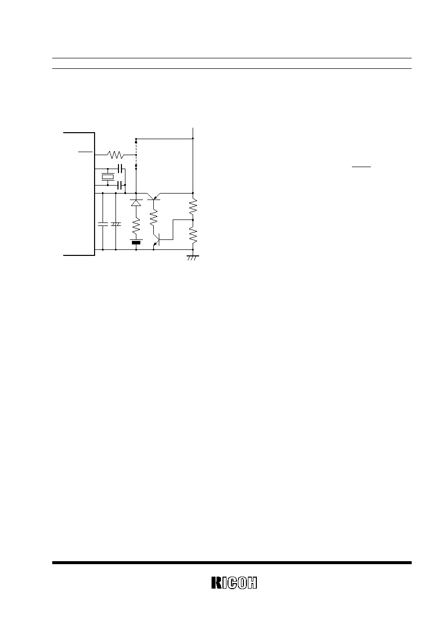
8. Typical Power Supply Circuit
OSCIN
OSCOUT
VDD
VSS
RP/RF/RS5C62
Voltage of system
power supply
A
B
INTR
1) Connect either one end of the oscillatory capacitors C
G
and C
D
to the VDD pin.
2) Install the by-pass capacitors for both high and low fre-
quencies in close proximity to the IC in such a manner
as to form a parallel arrangement.
3) Connect the pull-up resistor of the INTR pin to differ-
ent points depending on whether it is used while the
CE pin is held low (in battery backup).
(I) Connect the pull-up resistor to Point A in the left
circuit diagram unless it is used while the CE pin
is held low.
(II) Connect the pull-up resistor to Point B in the left
circuit diagram if it is used while the CE pin is
held low.
26
RP/RF/RS5C62
9. Typical Connection between RP/RF/RS5C62 and CPU
Z80
A4 to A15
A3 to A0
D3 to D0
RP/RF/RS5C62
Address
Decoder
Powerdown
Detector
IORQ
RD
WR
A3 to A0
D3 to D0
CS
RD
WR
CE
6809
A4 to A15
A3 to A0
D3 to D0
RP/RF/RS5C62
Address
Decoder
Powerdown
Detector
BS
BA
R/W
E
A3 to A0
D3 to D0
CS
RD
WR
CE
Address
Decoder
8086
ALE
A0 to A19
Latch
A0 to A19
AD0 to 15
RP/RF/RS5C62
Powerdown
Detector
RD
WR
A3 to A0
D3 to D0
CS
BHE
BHE
RD
WR
CE
68000
A1 to A23
D3 to D0
RP/RF/RS5C62
Powerdown
Detector
R/W
LDS
WR
BG
A3 to A0
D3 to D0
CS
RD
WR
CE
Address
Decoder
RP/RF/RS5C62 and CPU Z80
RP/RF/RS5C62 and CPU 6809
RP/RF/RS5C62 and CPU 8086
RP/RF/RS5C62 and CPU 68000
27
RP/RF/RS5C62
10. Typical Characteristics
10.3 Current Consumption vs. VDD
10.1 Current Consumption vs. CD
10.2 Current Consumption vs. CG
10.4 Current Consumption vs. Temperature
0
0
1
2
3
4
V
DD
=3V
C
D
(pF)
10
20
30
40
C
u
r
r
e
n
t
C
o
n
s
u
m
p
t
i
o
n
I
D
D
(
Ķ
A
)
C
D
= 5pF
C
D
=10pF
C
D
=20pF
C
D
=30pF
C
D
=39pF
0
0
1
2
3
4
Topt=25įC
C
G
=C
D
=10pF
V
DD
(V)
1
2
3
4
6
5
C
u
r
r
e
n
t
C
o
n
s
u
m
p
t
i
o
n
I
D
D
(
Ķ
A
)
0
0
1
2
3
4
V
DD
=3V
C
G
(pF)
10
20
30
40
C
u
r
r
e
n
t
C
o
n
s
u
m
p
t
i
o
n
I
D
D
(
Ķ
A
)
C
D
= 5pF
C
D
=10pF
C
D
=20pF
C
D
=30pF
C
D
=39pF
≠40
0
1
2
3
4
V
DD
=3V
C
G
=C
D
=10pF
Temperature Topt(įC)
≠20
0
20
40
80
60
C
u
r
r
e
n
t
C
o
n
s
u
m
p
t
i
o
n
I
D
D
(
Ķ
A
)
A
OSCIN
VDD
C
G
C
D
X'tal
OSCOUT
VDD
VSS
Frequency
counter
INTR
C
D
=10pF, C
G
=10pF
X'tal : RL
≤
35k
Ĺ
Topt=25įC
Input pin : VDD or VSS
Output pin : Open
28
RP/RF/RS5C62
10.7 Oscillation Frequency vs. V
DD
10.5 Oscillation Frequency vs. CG
10.6 Oscillation Frequency vs. CD
10.8 Oscillation Frequency vs. Temperature
0
≠100
≠40
≠20
≠60
≠80
0
20
40
60
80
f0:C
G
=C
D
=10pF
V
DD
=3V
C
G
(pF)
10
20
30
40
D
f
/
f
o
(
p
p
m
)
C
D
=10pF
C
D
=20pF
C
D
=30pF
C
D
= 5pF
0
≠4
≠3
≠1
≠2
0
1
f0:V
DD
=4V
C
G
=C
D
=10pF
V
DD
(V)
1
2
3
4
6
5
D
f
/
f
o
(
p
p
m
)
0
≠100
≠40
≠20
≠60
≠80
0
20
40
60
80
f0:C
G
=C
D
=10pF
V
DD
=3V
C
D
(pF)
10
20
30
40
D
f
/
f
o
(
p
p
m
)
C
D
=10pF
C
D
=20pF
C
D
=30pF
C
D
= 5pF
≠20
≠70
≠60
≠50
≠20
≠10
≠40
≠30
0
10
f0:Topt=22.5įC
V
DD
=3V,C
G
=C
D
=10pF
Topt(įC)
0
20
40
80
60
D
f
/
f
o
(
p
p
m
)
10.9 Oscillation Start Time vs. C
G
10.10 Nch Open Drain Output I
DS
vs.V
DS
0
≠4
0.5
1.5
1
2
2.5
3
V
DD
=3V
C
G
(pF)
10
20
30
40
O
s
c
i
l
l
a
t
i
o
n
s
t
a
r
t
t
i
m
e
(
s
)
C
D
= 5pF
C
D
=10pF
C
D
=20pF
C
D
=30pF
C
D
=39pF
0
0
5
15
10
20
25
30
35
V
DS
(V)
0.5
1
1.5
2
I
D
S
(
m
A
)
V
DD
=3V
V
DD
=5V
29
RP/RF/RS5C62
11. Typical Software-controlled Processes
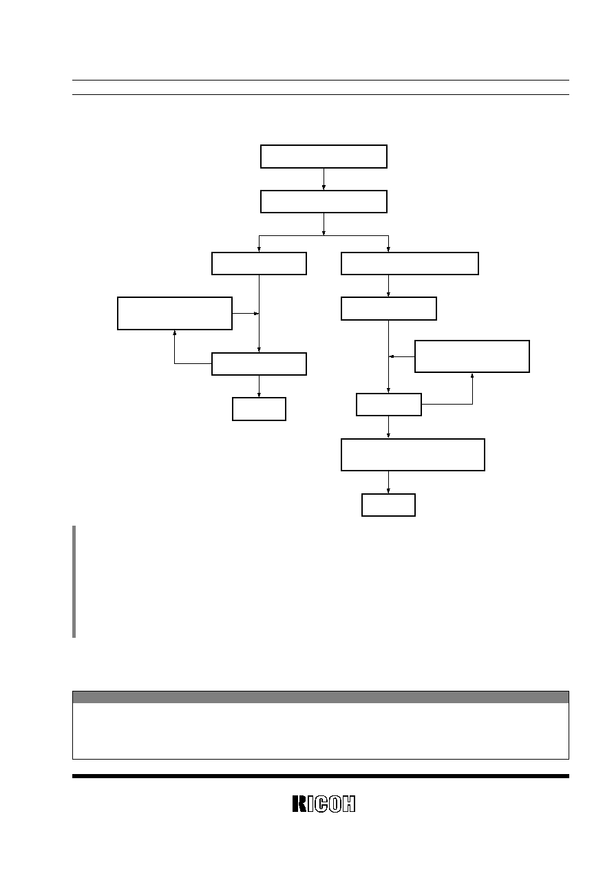
11.1 Initialization at Power-on
At power-on from 0V, the internal registers and the output pins have indefinite states and therefore require initial-
ization. The process of initialization differs as exemplified below depending on whether the XSTP bit (oscillation
stop detection bit) is set in the control register 2. In the latter typical process of initialization below, the XSTP bit is
used to check the validity of internal time data and the presence or absence of the initial routine.
11.1-1 Initialization Subject to No Setting of XSTP Bit
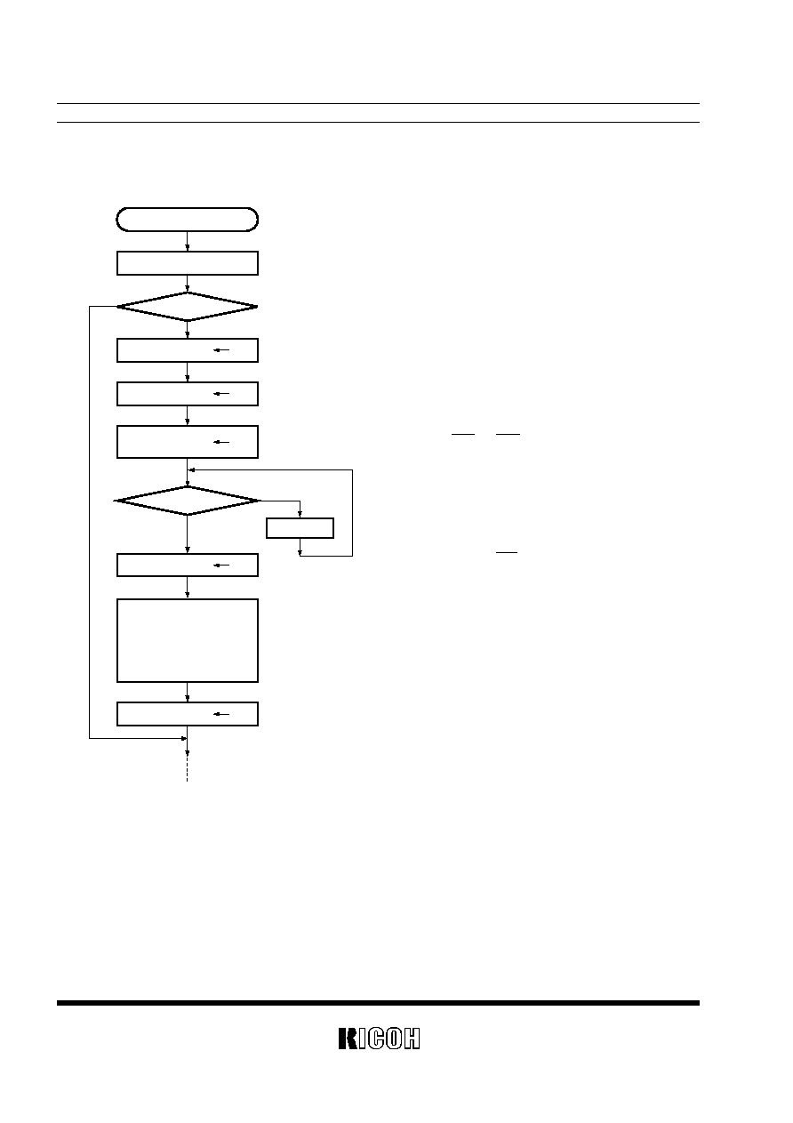
Start
Power-on from 0V
Timer clock
selection register
Interrupt cycle
selection register
Wait
YES
NO
BSY=0?
Set 12-hour or 24-hour time
scale, time and calendar
counters, interrupt cycles,
and timer output cycles
Control register 3
Fh
Control register 1
3h
Control register 2
0h
Control register 1
Fh
0h
0h
*
2
*
1
*
3
*
4
*
5
*
6
*
1) At power-on from 0V, the internal registers and the output pins have
indefinite states.
*
2) Set both the TSTA and TSTB bits and the WTRST bit to "1" in the control
register 3 and thereby set the BSY bit to"1" in the control register 2.
*
3) Set the WTEN bit to "0" (clock operation disabled), the ALEN bit to "0"
and TMR bit to "1" ( turn off the output pins) and the BANK bit to "1" in
the control register 1.
*
4) Drive high (turn off) the INTR and TMOUT pin outputs.
*
5) Check the BSY bit in the control register 2 for the dual purpose of con-
firming the absence of a carry and confirming the start of oscillation. This
requires additional time to wait for the start of the crystal oscillators. Fur-
ther, assign a time-out period to exit from the loop for checking the BSY
bit.
*
6) Start both the clock and alarm functions.
*
7) This typical process of initialization is applied at power-on from 0V and
not required at start-up from the backup battery.
RP/RF/RS5C62
30
11.1-2 Initialization Subject to Setting of XSTP Bit
Start
Power-on from 0V
Interrupt cycle
selection register
Wait
YES
YES
NO
BSY=0?
Set 12-hour or 24-hour
time scale, time and
calendar counters,
interrupt cycles, and timer
output cycles
Control register 3
Fh
Control register 1
3h
Control register 1
Fh
0h
*
2
*
1
*
3
*
4
*
5
Control register 2
0h
*
7
*
6
*
9
*
8
XSTP=0?
NO
*
1) At power-on from 0V, the internal registers and the output pins have
indefinite states.
*
2) Check the validity of internal time data.
In using the XSTP bit, ensure error-free detection of the stop of oscilla-
tion by:
1) Preventing the crystal oscillators causing condensation.
2) Preventing the VDD pin input from making instantaneous power dis-
connection.
3) Preventing the crystal oscillators from causing noises on the PCB (by
such means as signal line isolation).
4) Preventing the individual pins from being impressed with voltage
exceeding the maximum rating.
*
3) Set both the TSTA and TSTB bits and the WTRST bit to "1" in the control
register 3 and thereby set the BSY bit to "1" in the control register 2.
*
4) Set the WTEN bit to "0" (clock operation disabled), the ALEN bit to "0"
and TMR bit to "1" ( turn off the output pins) and the BANK bit to "1" in
the control register 1.
*
5) Drive high (turn off) the INTR pin output.
*
6) Wait for the start of the crystal oscillators to confirm the start of oscillation
as well as the absence of a carry. Further, assign a time-out period to
exit from the loop for checking the BSY bit.
*
7) Set the XSTP bit to "0" in the control register 2.
*
8) Start both the clock and alarm functions.
*
9) This route is applied at start-up from the backup battery when the process
of initialization is omitted, assuming no internal time data destruction.
RP/RF/RS5C62
31
11.2 Writing to or Reading from Time and Calendar Counters
11.2-1 Writing to or Reading from Time and Calendar Counters by Stopping Time Count Operation
(by Setting WTEN and checking BSY bits)
Set 12- or 24-hour
time scale
Wait
YES
NO
BSY=0?
WTEN
BANK
0
0
*
1
*
2
*
3
*
5
*
4
Write to or read from time
and calendar counters
WTEN
1
*
6
*
1) Set the 12- or 24-hour time scale once before writing to the time and cal-
endar counters (at the time of initialization after power-on from 0V).
*
2) Set the WTEN bit to "0" in the control register 1 to stop the second and
higher-order digits.
*
3) When the BSY bit is set to "1" in the control register 2, continue reading
from the time and calendar counters until it is set to "0" or wait for 122.1
Ķs or more. When the BSY bit is set to "0", it is kept at "0" until the
WTEN bit is set to "1" again in the control register 1.
*
4) Writing to the 1-year or 10-year counter automatically enables leap year
indication. To disable leap year indication, write "4h" (set the LYE bit to
"1" ) in the leap year indication register after setting the time and calen-
dar counters. Note that leap year indication is continued without correc-
tion until the year 2099.
*
5) When reading from the time and calendar counters, ensure that this route
lasts within 1 second. If this route lasts within 1 second, the 1-second
digit is incremented by 1 to correct a 1-second carry occurring during
read operation upon setting the WTEN bit to "1" again in the control reg-
ister 1. Note that the 1-second digit is also incremented by 1 to correct
more than one 1-second carry while the WTEN bit is kept at "0", resulting
in a clock delay.
*
6) Restart time count operation. (The WTEN bit will automatically be set to
"1" in the control register 1 upon driving low the CE pin.)
*
7) When writing to the time and calendar counters, be sure to check the
BSY bit in the control register 2 by disabling a carry (by setting the
WTEN bit to "0" ).
Writing to the time and calendar counters must be performed in the absence of a carry. In particular, correct
writing to the time and calendar counters requires stopping time count operation (by setting that the WTEN bit to
"0" in the control register 1) and confirming the absence of a carry (by checking that the BSY bit to "0" in the con-
trol register 2). On the other hand, reading from the time and calendar counters may be performed by stopping
time count operation, generating a cyclic interrupt, or dual reading.
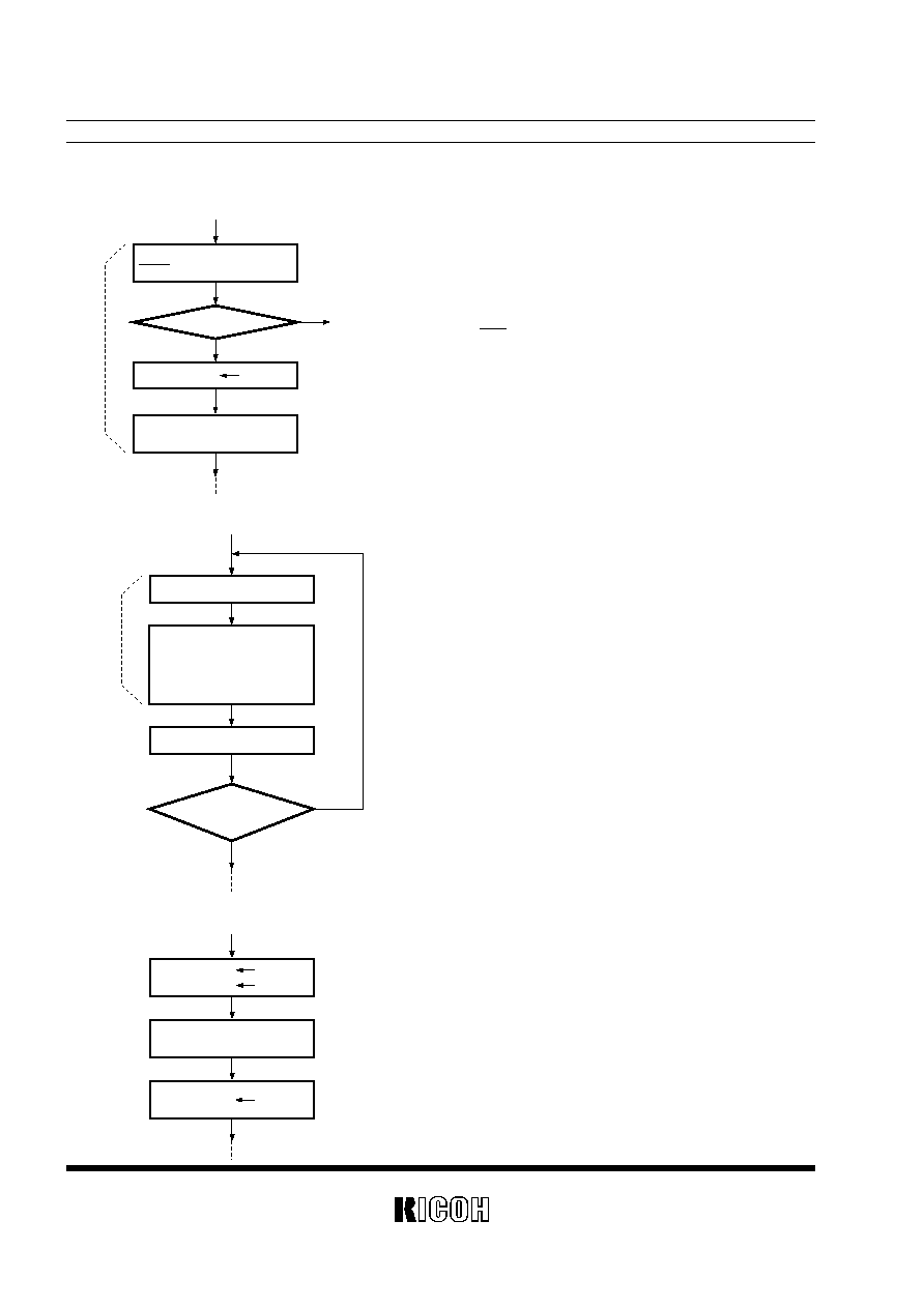
RP/RF/RS5C62
32
11.2-2 Reading from Time and Calendar Counters by Generating Cyclic Interrupt
YES
NO
Proceed to
interrupt from
other ICs
CTFG=0?
Output cyclic interrupt from
INTR pin
*
1
CTFG
0
Read from time and
calendar counters
This typical process of reading from the time and calendar
counters is applied on the conditions below:
1) The INTR pin is set to the level mode (upon setting the CT
3
to "1" in the
interrupt cycle selection register).
2) The route marked with "
*
1" lasts within the time equivalent to a preset
cycle minus 30.5Ķs (for the purpose of preventing occurrence of an error
due to a carry during reading from the time and calendar counters).
11.2-3 Reading from Time and Calendar Counters by Dual Reading
YES
NO
Dual readings
match?
*
1
*
2
Read 1-second digit
Read 1-second digit again
Read from the time and
calendar counters (starting
with address "1h" and
ending with address "Ch")
*
1) A carry from the second digit starts with 1 second via 10 seconds,---and
1 year, and ends with 10 years. Consequently, reading from the time
and calendar counters must also start with the 10-second digit (at
address "1h" ) and end with the 10-year digit (at address "Ch" ).
*
2) This route assumes that an error occurs due to a carry during reading
from the time and calendar counters.
11.3 Writing Alarm Time to Alarm Registers
Write alarm time
(in minutes and hours)
ALEN
BANK
0
1
ALEN
1
*
1
*
1) Non-existent alarm time may be set in the alarm register, provided that an
alarm interrupt is disabled. To enable an alarm interrupt, existent alarm
time must be set in the alarm register.
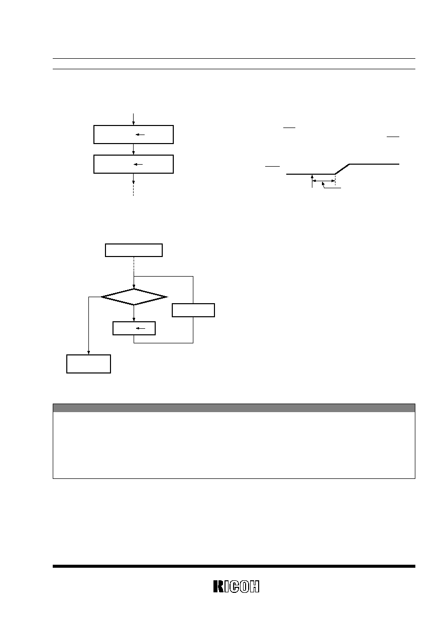
RP/RF/RS5C62
33
11.4 Adjusting Second Digit by Ī30 Seconds
BANK
1
ADJ
1
*
1
*
2
*
1) Upon setting the ADJ bit to "1" in the adjustment register, the second and
lower-order 1 to 8Hz dividers are reset conditional on restart. At this
time, when the INTR pin is held low for output of a cyclic interrupt with a
cycle of 1 second or 60 seconds in the pulse mode, the INTR pin is
turned off with the timing shown below:
11.5 Detecting Start of Oscillation
NO
YES
XSTP=0
*
1
*
2
*
3
Wait
Detect start of
oscillation
Power-on from 0V
0
XSTP
*
1) This typical process of detecting the start of oscillation is applied at pow-
er-on from 0V.
*
2) At power-on from 0V, the XSTP bit is set to "1" in the control register 2.
*
3) Note that the start of oscillation normally requires a time period (oscilla-
tion start time) on the order of 0.1 to 2 seconds. Further, assign a time-
out period to exit from loop for checking the XSTP bit in the control regis-
ter 2.
L
OFF
Maximum of 200 Ķs
Setting the ADJ
bit to "1"
INTR
*
2) Adjustment of the second digit by Ī30 seconds requires a maximum of
122.1Ķs, during which the BSY bit is kept at "1" in the control register 2.
Notice
In using the XSTP bit, ensure error-free detection of the stop of oscillation by:
1) Preventing the crystal oscillators causing condensation.
2) Preventing the VDD pin input from making instantaneous power disconnection.
3) Preventing the crystal oscillators from causing noises on the PCB (by such means as signal line isolation).
4) Preventing the individual pins from being impressed with voltage exceeding the maximum rating.
Question 1 : What are the causes of failure in adjustment of oscillation frequencies? (Subject to use of
variable capacitors and adjustment of oscillation frequencies)
Question 2 : What are the causes of inaccurate time count operation? (Subject to use of fixed capaci-
tors and no adjustment of oscillation frequencies)
RP/RF/RS5C62
34
QUESTIONS AND ANSWERS ON USE
Below are listed questions and answers on using the RP/RF/RS5C62 under the following four categories:
1) Crystal oscillators
2) Hardware
3) Software
4) AC/DC electrical characteristics and others
Answer 1: For capacitance variations of about 5 to 30pF, oscillation frequency variations measure a little
more than about 60ppm in real terms (see the graphs in 10.5 and 10.6 of "10. Typical
Characteristics"). The possible causes of failure in adjustment of oscillation frequencies are :
1. Variations in the crystals, the capacitors, and the ICs outside the range of adjustment of
capacitance variations, and
2. Mismatching between the central value of variations in these elements and that of the range
of variations of variable capacitors.
The possible corrective measures for the causes 1. and 2. above are :
1. Reviewing variations in the individual elements. (For reference, measurements of variations
in the ICs are shown in Answer 3 below.), and
2. Adjusting oscillation frequencies according to the directions described in "4. Adjustment of
Oscillation Frequencies" in "USAGE".
Answer 2: The possible causes of inaccurate time count operation are :
1. Mismatching between the capacitance of the oscillatory capacitors C
G
and C
D
and that of the
crystals and the ICs, and
2. Too great floating capacitance present on the actual PCB to be neglected for the oscillatory
capacitors C
G
and C
D
, which are adapted to the ICs and the ranking of oscillation frequencies
(load capacitance (C
L
)).
The possible corrective measures for the causes 1. and 2. above are :
1. Adjusting oscillation frequencies according to the directions described in "4. Adjustment of
Oscillation Frequencies" in "USAGE", and
2. Reduce the capacitance of the oscillatory capacitors C
G
and C
D
by the equivalent of floating
capacitance, which seems to vary from 1 to several pF depending on the layout of the PCB, or
mount them on the actual PCB for final fixing.
Category
Questions and Answers
1) Crystal
oscillators

Category
Questions and Answers
Question 3 : How many variation factors should be considered? (Subject to use of fixed capacitors and
no adjustment of oscillation frequencies)
RP/RF/RS5C62
35
1. The possible factors behind oscillation frequency variations are :
1-1. Variations in frequencies of crystals,
1-2. Variations in oscillation characteristics of the ICs,
1-3. Variations in the external oscillatory capacitors C
G
and C
D
, and
1-4. Variations in floating capacitance present on the actual PCB.
2. On the other hand, the possible factors behind surrounding environment variations are :
2-1. Variations in ambient temperature, and
2-2. Variations in supply voltage.
Variations in 1 - 1 to 1 - 4 are listed in the order of decreasing degree. The individual variations
are described below :
1-1. Most crystals seem to have variations in their frequencies on the order of Ī20ppm while
some crystals may have smaller variations. For variations in frequencies of individual crys-
tals, inquire of their suppliers.
1-2. Sample measurements of variations in oscillation characteristics of the ICs are shown
graphically on the next page. Note that these measurements are not guaranteed ones and
are therefore intended for reference use only.
1-3. Variations in oscillation frequencies differ slightly depending on the capacitance of external
oscillatory capacitors C
G
and C
D
. More specifically, the smaller the capacitance of C
G
and
C
D
, the greater the variations in oscillation frequencies. Subject to no adjustment of oscilla-
tion frequencies, they should have small variations relative to their capacitance (see the
graphs in 10.5 and 10.6 of "10. Typical Characteristics").
1-4. Normally, variations in floating capacitance present on the actual PCB seem to be small
enough to be negligible.
2-1. Variations in ambient temperature are dominantly affected by the temperature characteris-
tics of fork-shaped crystal oscillators (forming an upward-facing quadratic curve) (see the
graph in 10.8 of "10. Typical Characteristics").
2-2. Because the oscillatory circuit inside the ICs is driven by constant voltage, Variations in
oscillation frequencies due to variations in supply voltage measureĪ0.5ppm or less on real
terms at room temperature with the VDD pin input ranging from 2.5V to 5.5V (see the
graph in 10.7 of "10. Typical Characteristics").
Category
Questions and Answers
Question 4 : Why should you avoid connecting either end of the oscillatory capacitors C
G
and C
D
to the
VSS pin instead of the VDD pin?
Question 5 : Synchroscopic observation of the OSCOUT pin output shows that it has an oscillatory
waveform having a small amplitude or approximating to the VDD pin input. What is the cause of this
phenomenon?
RP/RF/RS5C62
36
V
DD
Vp-p:Approx.
1.5 to 2.0V
Approx.
2.0V
V
SS
Internal constant voltage output
Sample Measurements of Variations in Oscillation Characteristics of ICs
V
DD
: 5V at room temperature
C
G
: Approx. 10.5pF, C
D
: Approx. 12.5pF
Total of 54 ICs sampled from 6 lots for measurement
Average variation: 0ppm
Standard deviation: 0.630ppm
Number of samples
5
0
10
≠10
≠5
0
LOT1
LOT2
LOT3
LOT4
LOT5
LOT6
5
10
15
20
25
30
ppm
Answer 4: Because the oscillatory circuit is driven by a constant voltage of 2V relative to the VDD pin,
either one end of the oscillatory capacitors C
G
and C
D
must be connected to the VDD pin with-
out exception. When either one end of the oscillatory capacitors C
G
and C
D
is connected to the
VSS pin instead of the VDD pin, the oscillatory circuit is still operational but subject directly to
fluctuations in the voltage of the system power supply. Under sharp fluctuations between 5V
and battery voltage in particular, the oscillatory circuit may be brought to a temporary stop.
Thus, it is not recommendable to connect either one end of the oscillatory capacitors C
G
and
C
D
to the VSS pin.
Answer 5: To reduce power consumption, the oscillatory circuit is driven by a constant voltage of about 2V
relative to the VDD pin, so that the OSCOUT pin output has an oscillatory waveform shown in
the figure below. Its amplitude will vary slightly depending on the capacitance of the oscillatory
capacitor C
D
. Note that the oscillatory waveform measurements on the OSCOUT pin cannot be
directly applied to adjustment of oscillation frequencies, which are shifted by use of a probe.
(For how to adjust oscillation frequencies, see "4. Adjustment of Oscillation Frequencies" in
"USAGE".)
Category
Questions and Answers
2) Software
Question 4 : An attempt to disable an alarm interrupt by setting the ALFG bit to "0" in the control regis-
ter 2 results in holding the INTR pin output low. What is the cause of this phenomenon?
Question 3 : How can the INTR pin output be used?
RP/RF/RS5C62
37
Answer 1: In the typical software-controller process of initialization at power-on from 0V, the BSY bit is set
to "1" in the control register 2 by setting the WTRST bit to "1" in the control register 3 for the
dual purpose of confirming the absence of a carry and confirming the start of oscillation. After
power-on from 0V, the start of oscillation normally requires a time period (oscillation start time)
on the order of 0.1 to 2 seconds, which, in turn, requires additional time to wait for the start of
the crystal oscillators. It seems most likely, therefore, that the BSY bit fails to be switched from
"1" to "0" due to prolonged oscillation start time. Further, another possibility is that the start of
oscillation may be hindered by some trouble (e.g. condensation) with the crystal oscillators. It
is necessary, therefore, to assign a time-out period to exit from the loop for checking the BSY
bit in the control register 2.
Answer 2: As described in "11. 2. 1. Writing to or Reading from Time and Calendar Counters by Stopping
Time Count Operation (by Setting WTEN and BSY Bits)", the WTEN bit in the control register
1 and the BSY bit in the control register 2 are used to read from the time and calendar counters
in such a manner as to prevent occurrence of an error due to a carry during read operation. If
the BSY bit is found to be "1", however, this typical software-controlled process involves addi-
tional time to wait for setting of the BSY bit to "0". To save such wait time, an alternative action
can be taken to read the 1-second digit twice without setting the WTEN and BSY bits as shown
in "11. 2. 3. Reading from Time and Calendar Counters by Dual Reading". This process fea-
tures dual reading from the 1-second digit in anticipation of an error which may occur due to a
carry during read operation from the time and calendar counters in case of mismatching
between the dual readings.
Answer 3: The INTR pin outputs an alarm interrupt and a cyclic interrupt. For details on these two types of
interrupts, see "5. Interrupts" in "USAGE".
Answer 4: The INTR pin outputs the logical sum (OR) of an alarm interrupt and a cyclic interrupt when
they are generated in combination. Consequently, an attempt to disable an alarm interrupt by
setting the ALFG bit to "0" may result in holding the INTR pin low when it outputs a cyclic inter-
rupt as well.
Question 1 : In the typical software-controlled process of initialization at power-on from 0V, the BSY bit
is checked to find that it fails to be switched from "1" to "0". What is the cause of this failure?
Question 2 : How is it possible to read from the time and calendar counters without setting the WTEN
and BSY bits?
Category
Questions and Answers
Question 5 : An attempt to disable a cyclic interrupt by setting the CTFG bit to "0" in the control regis-
ter 2 results in holding the INTR pin output low. What is the cause of this phenomenon?
Question 6 : What will happen if non-existent time is set?
Question 8 : How can an alarm interrupt be output on a monthly basis?
Question 7 : How can an alarm interrupt be used in battery backup? (Why is an alarm interrupt not out-
put in battery backup?)
Answer 6: Time or alarm digits which are non-existent or indicated in non-BCD notation can be set in the
time counter or the alarm register without causing any trouble. If such invalid digits are left,
however, they may cause faulty time count operation in case of a carry or mismatching between
clock time and alarm time.
RP/RF/RS5C62
38
Answer 5: As in Answer 4 above, this phenomenon may occur when an alarm interrupt and a cyclic inter-
rupt are simultaneously output from the INTR pin.
Answer 7: An alarm interrupt is normally output from the INTR pin in battery backup (while the CE pin is
held low). Its output is most likely to fail, therefore, when the other end of the pull-up resistor
of the INTR pin is connected to any power supply which may be turned off. To prevent this
problem, confirm that the other end of the pull-up resistor of the INTR pin is connected to the
backup battery.
Answer 8: The RP/RF/RS5C62 are configured to issue a daily alarm and cannot be reconfigured to gener-
ate an alarm interrupt on a monthly basis. Considering that they are designed to reduce cur-
rent consumption as described in "Note" below, an advisable alternative action is to generate an
alarm interrupt to the CPU on a daily basis and keep track of alarm dates in a software-con-
trolled process.
Note
: The RP/RF/RS5C62 are designed to reduce current consumption (ensure typical current con-
sumption on the order of 1ĶA for 3V). Daily current consumption can be calculated as follows :
Assuming, for example, that an alarm interrupt to the CPU is generated on a daily basis as the
CPU is operating for a period of 0.5seconds with peak current consumption of 20mA, daily cur-
rent consumption can be calculated from the equation : 0.5s
ī20mA/60ī60ī24 = 0.115ĶA. This
means a total base current of a little more than 1ĶA, a slight increase in current consumption.
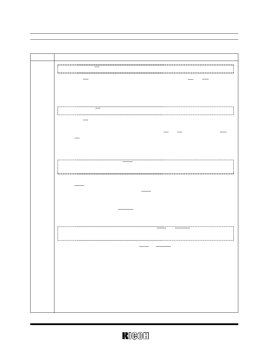
Category
Questions and Answers
3) Hardware
Question 3 : At power-on from 0V, the INTR pin is driven low to output interrupts. What is the cause of
this phenomenon?
Question 4 : As the N-channel open drain pins, may the INTR and TMOUT pins be impressed with
higher voltage than the VDD pin?
Question 1 : Can the CS pin input be used as it is held low?
Question 2 : May the CS pin input be driven low before or during the process of addressing?
Answer 4: As the N-channel open drain pins, the INTR and TMOUT pins, neither of which incorporates a
protective diode for the VDD pin, may be impressed with higher voltage than the VDD pin as
long as it does not exceed the maximum absolute rating of 12V. Their on-state resistance typi-
cally ranges from a few dozen ohms to one hundred ohms (see the graph in 10.10 of "10.
Typical Characteristics"). Their on-state current should preferably range from 10mA to 20mA
or less and must not exceed the maximum current consumption for the package.
Answer 3: At power-on from 0V, the internal registers and counters have indefinite states, causing the
INTR pin to have indefinite states as well. It is necessary, therefore, to provide temporary
masking for interrupts output from the INTR pin and initialize the internal registers and coun-
ters by following the typical software-controlled processes of initialization at power-on (see "11.
1 Initialization at Power-on"). (At power-on from 0V, when the XSTP bit is set to "1" to indicate
the start of oscillation, the TMOUT pin output is turned off.)
Answer 2: The CS pin input may be driven low before, during, or even after the process of addressing.
Addressing time (
t
AS
) indicates the time required to perform the process of addressing before
the start of read or write operation at which both the RD and CS pin inputs or both the WR and
CS pin inputs are driven low. For more details, see "1. Reading and Writing Operations" in
"USAGE".
RP/RF/RS5C62
39
Answer 1: The CS pin input can be used as it is held low, provided that the RD and WR pin inputs are
caused to transition from their high to low to high levels to enable read and write operations,
respectively.
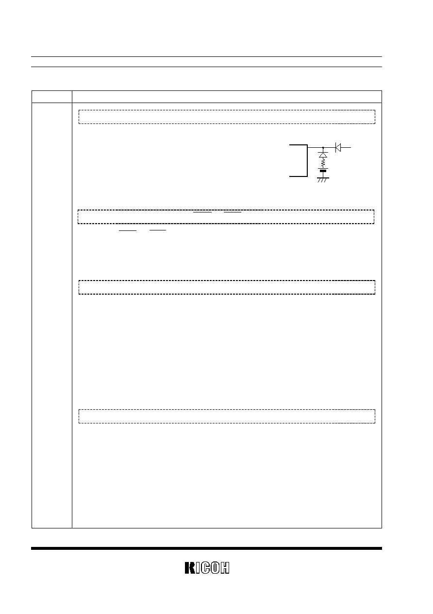
Category
Questions and Answers
Question 5 : Is it possible to configure a power switching circuit containing a diode?
Question 6 : To what test modes can the TSTA and TSTB bits be applied as test bits?
Question 7 : What are the possible causes of any changes which may occur to internal time data?
Question 8 : What are the ranges of operating voltages?
RP/RF/RS5C62
40
Answer 6: The TSTA and TSTB bits are intended for IC selection and not for general users. (These test
bits should be kept at "1" in normal operation and will automatically be set to "1" upon driving
low the CE pin.)
Answer 5: It is not recommendable to configure a power switch-
ing circuit containing a diode, which causes a voltage
drop as shown in the right circuit diagram (where
"D
1
" represents a diode). (The maximum absolute
ratings of the input and output pins range from ≠0.3V
to the V
DD
plus 0.3V.)
VDD
D
1
System
power
supply
RP/RF/RS5C62
Answer 7: The possible causes of such changes include :
1. Occurrence of writing errors due to such factors as noises caused below the operating volt-
age of the CPU at the time of switching from the power supply to the backup battery,
2. Occurrence of instantaneous power disconnection, and
3. Writing to other addresses than are allocated originally due to shortage of addressing time
(
t
AS
).
To cope with the cause 1. , see "2. Handling of CE Pin" in "USAGE". To solve the cause 2. ,
check the power supply system to prevent instantaneous power disconnection from occur-
ring. To overcome the cause 3. , secure sufficient addressing time (
t
AS
).
Answer 8: Range of operating voltage of crystal oscillators only for time count operation: 2.0V to 6.0V.
Range of operating voltage having any access to the CPU : 2.7V to 6.0V
Incidentally, AC timing is available in three ratings : 3VĪ10%, 5VĪ10%, and 5VĪ20%.
Question 1 : What is the difference between backup current consumption and standby current con-
sumption?
Question 2 : How is it possible to know typical backup current consumption and temperature character-
istics in determining the battery capacity?
Question 3 : What is the cause of partial mismatching of AC timing with the high-speed CPU?
Question 4 : Is it possible to extend the operating temperature range of ≠20įC to +70įC?
RP/RF/RS5C62
41
Answer 1: Backup current consumption is defined as current consumption in battery backup with the CE
pin held low (connected to the V
SS
input) and the other pins opened (the term "opened" also
refers to "impressed with intermediate voltage"). On the other hand, standby current consump-
tion is defined as current consumption in the absence of access from the CPU with the CE and
CS pins held high (connected to the V
DD
pin input) and the other input pins connected to the
V
DD
or V
SS
pin input and the other output pins opened. The V
DD
pin input is set to 2.5V for
backup current consumption and 5.5V for standby current consumption.
Answer 2: For typical backup current consumption and temperature characteristics, see the graphs in 10. 1
to 10.4 in "10. Typical Characteristics".
Answer 3: AC timing is designed to secure margins including variations and therefore difficult to change in
principle, provided that it is susceptible to change, as the case may be, upon request.
Answer 4: As in Answer 3 above, the operating temperature range is difficult to change in principle, provid-
ed that it is susceptible to change, as the case may be, upon request.
Category
Questions and Answers
4) AC/DC
electric
character-
istics and
others
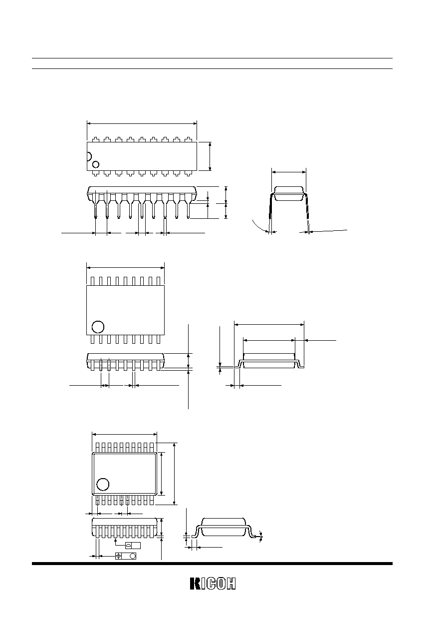
42
RP/RF/RS5C62
PACKAGE DIMENSIONS
(Unit: mm/(inch))
∑
RP5C62 (18pin DIP)
∑
RF5C62 (18pin SOP)
∑
RS5C62 (20pin SSOP)
0
to
15į
24.8MAX.
7.62TYP.
(0.300TYP.)
2.54TYP.
(0.100TYP.)
(0.300TYP.)
1.5TYP.
6
.
6
M
A
X
.
M
I
N
.
0
.
5
1
(
0
.
1
8
5
M
A
X
.
)
(
0
.
1
1
0
M
A
X
.
)
(
0
.
2
5
9
M
A
X
.
)
(0.976MAX.)
18
10
1
9
0.46
+0.15
≠0.1
(0.018 )
+0.006
≠0.004
0.25
+0.15
≠0.05
(0.010 )
+0.006
≠0.002
(
0
.
0
2
0
)
M
I
N
.
4
.
7
M
A
X
.
2
.
8
M
I
N
.
11.84MAX.
1.27TYP.
(0.050TYP.)
0
.
2
Ī
0
.
1
(
0
.
0
0
8
Ī
0
.
0
0
1
)
2
.
3
4
T
Y
P
.
(
0
.
0
9
2
T
Y
P
)
(0.466MAX.)
10.31Ī0.3
(0.406Ī0.012)
7.49TYP.
(0.295TYP.)
1.4TYP.
(0.056TYP.)
0.66Ī0.2
(0.026Ī0.008)
10
9
18
1
0
.
2
5
+
0
.
1
≠
0
.
0
5
(
0
.
0
1
0
)
+
0
.
0
0
4
≠
0
.
0
0
2
0.41TYP
+0.1
≠0.05
(0.016TYP )
+0.001
≠0.002
0.65
1
10
11
20
0.22Ī0.1
0.5Ī0.2
0 to10į
1
.
1
5
Ī
0
.
1
4
.
4
Ī
0
.
2
6
.
4
Ī
0
.
3
0
.
1
Ī
0
.
1
0
.
1
5
+
0
.
1
≠
0
.
0
5
6.5
+0.3
≠0.1
0.45MAX.
0.1
M
0.1
RP/RF/RS5C62
43
TAPING SPECIFICATIONS
(Unit: mm)
∑
RF5C62 (18pin SOP)
E1
E2
User Direction of Feed.
12Ī0.1
11.05
4.0Ī0.1
2.0Ī0.1
0.3Ī0.05
3.35Ī0.1
2
4
Ī
0
.
3
1
1
.
5
Ī
0
.
1
1
3
.
2
1
.
7
5
Ī
0
.
1
Ý1.55Ī0.05
∑
RS5C62 (20pin SSOP)
E1
E2
User Direction of Feed.
8.0Ī0.1
6.7
4.0Ī0.1
2.0Ī0.05
0.3Ī0.1
2.7MAX.
1
2
.
0
Ī
0
.
3
5
.
5
Ī
0
.
0
5
6
.
9
1
.
7
5
Ī
0
.
1
Ý1.5
+0.1
≠0

RICOH COMPANY, LTD.
ELECTRONIC DEVICES DIVISION
HEADQUARTERS
13-1, Himemuro-cho, Ikeda City, Osaka 563-8501, JAPAN
Phone 81-727-53-1111 Fax 81-727-53-6011
YOKOHAMA OFFICE (International Sales)
3-2-3, Shin-Yokohama, Kohoku-ku, Yokohama City, Kanagawa 222-8530,
JAPAN
Phone 81-45-477-1697 Fax 81-45-477-1694 ∑ 1695
http://www.ricoh.co.jp/LSI/english/
RICOH CORPORATION
ELECTRONIC DEVICES DIVISION
SAN JOSE OFFICE
3001 Orchard Parkway, San Jose, CA 95134-2088, U.S.A.
Phone 1-408-432-8800 Fax 1-408-432-8375